 | –≠–ª–µ–∫—Ç—Ä–æ–Ω–Ω—ã–π –∫–æ–º–ø–æ–Ω–µ–Ω—Ç: OPA690 | –°–∫–∞—á–∞—Ç—å:  PDF PDF  ZIP ZIP |
FEATURES
D
HIGH BANDWIDTH:
250MHz (G = +1)
110MHz (G = +2)
D
LOW SUPPLY CURRENT: 3.9mA (V
S
= +5V)
D
FLEXIBLE SUPPLY RANGE:
±
1.4V to
±
5.5V Dual Supply
+2.8V to +11V Single Supply
D
INPUT RANGE INCLUDES GROUND ON
SINGLE SUPPLY
D
4.88V OUTPUT SWING ON +5V SUPPLY
D
HIGH SLEW RATE: 550V/ns
D
LOW INPUT VOLTAGE NOISE: 9.2nV/
Hz
D
Pb-FREE SOT23 PACKAGE
APPLICATIONS
D
SINGLE-SUPPLY ANALOG-TO-DIGITAL
CONVERTER (ADC) INPUT BUFFERS
D
SINGLE-SUPPLY VIDEO LINE DRIVERS
D
CCD IMAGING CHANNELS
D
LOW-POWER ULTRASOUND
D
PLL INTEGRATORS
D
PORTABLE CONSUMER ELECTRONICS
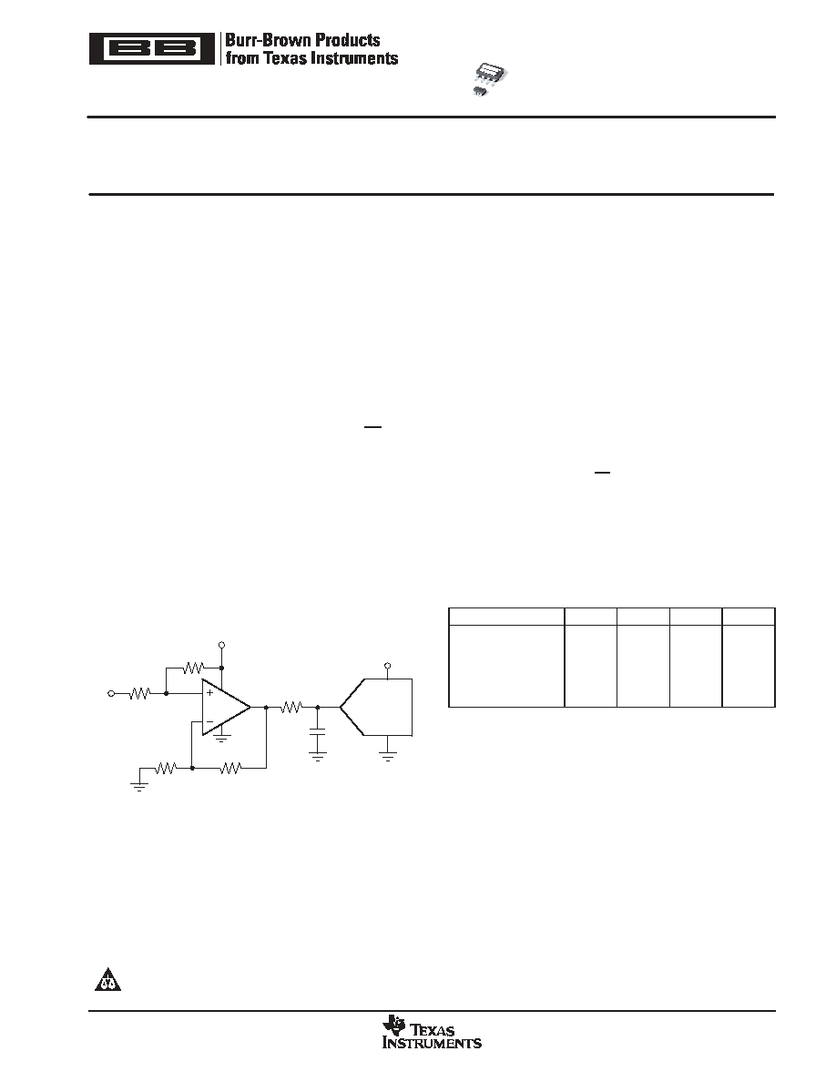
OPA830
V
IN
750
562
2.26k
374
22pF
+3V
100
+3V
THS1040
10-Bit
30MSPS
DC-Coupled, +3V ADC Driver
DESCRIPTION
The OPA830 is a low-power, single-supply, wideband,
voltage-feedback amplifier designed to operate on a single
+3V or +5V supply. Operation on
±
5V or +10V supplies is also
supported. The input range extends below the negative
supply and to within 1.7V of the positive supply. Using
complementary common-emitter outputs provides an output
swing to within 25mV of either supply while driving 150
. High
output drive current (
±
80mA) and low differential gain and
phase errors also make them ideal for single-supply
consumer video products.
Low distortion operation is ensured by the high gain
bandwidth product (110MHz) and slew rate (550V/
µ
s), making
the OPA830 an ideal input buffer stage to 3V and 5V CMOS
ADCs. Unlike other low-power, single-supply amplifiers,
distortion performance improves as the signal swing is
decreased. A low 9.2nV/
Hz input voltage noise supports
wide dynamic range operation.
The OPA830 is available in an industry-standard SO-8
package. The OPA830 is also available in an ultra-small
SOT23-5 package. For fixed-gain line driver applications,
consider the OPA832.
RELATED PRODUCTS
DESCRIPTION
SINGLES
DUALS
TRIPLES
QUADS
Rail-to-Rail
--
OPA2830
--
OPA4830
Rail-to-Rail Fixed Gain
OPA832
OPA2832
OPA3832
--
General-Purpose
(1800V/
µ
s slew rate)
OPA690
OPA2690
OPA3690
--
Low-Noise,
High DC Precision
OPA820
OPA2822
--
OPA4820
OPA830
SBOS263B - AUGUST 2004 - REVISED JANUARY 2005
Low-Power, Single-Supply, Wideband
Operational Amplifier
PRODUCTION DATA information is current as of publication date. Products
conform to specifications per the terms of Texas Instruments standard warranty.
Production processing does not necessarily include testing of all parameters.
www.ti.com
Copyright
2004-2005, Texas Instruments Incorporated
Please be aware that an important notice concerning availability, standard warranty, and use in critical applications of Texas Instruments
semiconductor products and disclaimers thereto appears at the end of this data sheet.
All trademarks are the property of their respective owners.
OPA830
SBOS263B - AUGUST 2004 - REVISED JANUARY 2005
www.ti.com
2
ABSOLUTE MAXIMUM RATINGS
(1)
Power Supply
12VDC
. . . . . . . . . . . . . . . . . . . . . . . . . . . . . . . . . . . . .
Internal Power Dissipation
See Thermal Analysis
. . . . . . . . . . . . . .
Differential Input Voltage
±
1.2V
. . . . . . . . . . . . . . . . . . . . . . . . . . . . .
Input Voltage Range (Single Supply)
-0.5V to +VS + 0.3V
. . . . . . .
Storage Temperature Range: D, DBV
-40
∞
C to +125
∞
C
. . . . . . . . .
Lead Temperature (soldering, 10s)
+300
∞
C
. . . . . . . . . . . . . . . . . . . .
Junction Temperature (TJ)
+150
∞
C
. . . . . . . . . . . . . . . . . . . . . . . . . . .
ESD Rating:
Human Body Model (HBM)
2000V
. . . . . . . . . . . . . . . . . . . . . . .
Charge Device Model (CDM)
1500V
. . . . . . . . . . . . . . . . . . . . .
Machine Model (MM)
200V
. . . . . . . . . . . . . . . . . . . . . . . . . . . . . .
(1) Stresses above these ratings may cause permanent damage.
Exposure to absolute maximum conditions for extended periods
may degrade device reliability. These are stress ratings only, and
functional operation of the device at these or any other conditions
beyond those specified is not supported.
This integrated circuit can be damaged by ESD. Texas
Instruments recommends that all integrated circuits be
handled with appropriate precautions. Failure to observe
proper handling and installation procedures can cause damage.
ESD damage can range from subtle performance degradation to
complete device failure. Precision integrated circuits may be more
susceptible to damage because very small parametric changes could
cause the device not to meet its published specifications.
PACKAGE/ORDERING INFORMATION
(1)
PRODUCT
PACKAGE-LEAD
PACKAGE
DESIGNATOR
SPECIFIED
TEMPERATURE
RANGE
PACKAGE
MARKING
ORDERING
NUMBER
TRANSPORT
MEDIA, QUANTITY
OPA830
SO-8 Surface-Mount
D
-40
∞
C to +85
∞
C
OPA830
OPA830ID
Rails, 100
OPA830IDR
Tape and Reel, 2500
OPA830
SOT23-5
DBV
-40
∞
C to +85
∞
C
A72
OPA830IDBVT
Tape and Reel, 250
OPA830IDBVR
Tape and Reel, 3000
(1) For the most current package and ordering information, see the Package Option Addendum at the end of this document, or see the TI website
at www.ti.com.
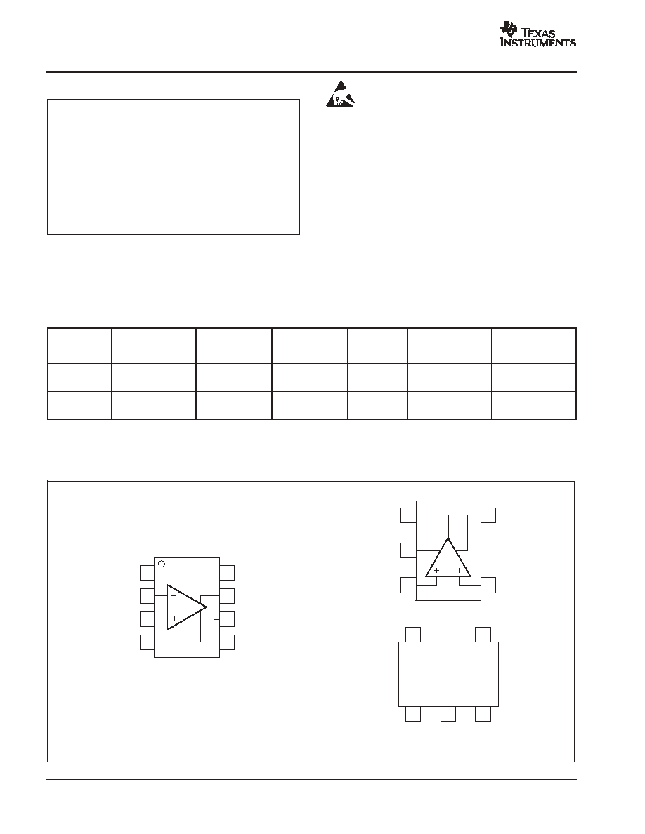
PIN CONFIGURATIONS
1
2
3
5
4
Output
-
V
S
Noninverting Input
+V
S
Inverting Input
A72
1
2
3
5
4
Pin Orientation/Package Marking
SOT23-5
1
2
3
4
8
7
6
5
NC
Inverting Input
Noninverting Input
-
V
S
NC
+V
S
Output
NC
SO-8
NC = No Connection

OPA830
SBOS263B - AUGUST 2004 - REVISED JANUARY 2005
www.ti.com
3
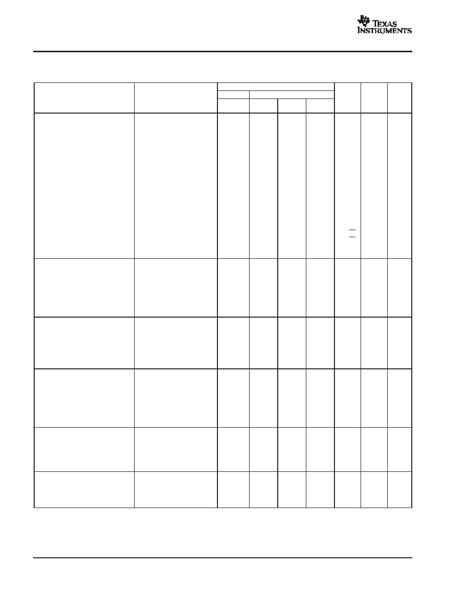
ELECTRICAL CHARACTERISTICS: V
S
=
±
5V
Boldface limits are tested at +25
∞
C.
At TA = 25
∞
C, G = +2, RF = 750
, and RL = 150
to GND, unless otherwise noted (see Figure 3).
OPA830ID, IDBV
TYP
MIN/MAX OVER TEMPERATURE
TEST
PARAMETER
CONDITIONS
+25
∞
C
+25
∞
C(1)
0
∞
C to
70
∞
C(2)
-40
∞
C to
+85
∞
C(2)
UNITS
MIN/
MAX
TEST
LEVEL
(3)
AC PERFORMANCE (see Figure 3)
Small-Signal Bandwidth
G = +1, VO
0.2VPP
310
MHz
typ
C
G = +2, VO
0.2VPP
120
70
68
65
MHz
min
B
G = +5, VO
0.2VPP
25
18
16
15
MHz
min
B
G = +10, VO
0.2VPP
11
8
7
6
MHz
min
B
Gain-Bandwidth Product
G
+10
110
85
82
80
MHz
min
B
Peaking at a Gain of +1
VO
0.2VPP
6
dB
typ
C
Slew Rate
G = +2, 2V Step
600
280
270
260
V/
µ
s
min
B
Rise Time
0.5V Step
3.3
5.8
5.85
5.9
ns
max
B
Fall Time
0.5V Step
3.5
5.9
5.95
6.0
ns
max
B
Settling Time to 0.1%
G = +2, 1V Step
42
63
65
66
ns
max
B
Harmonic Distortion
VO = 2VPP, f = 5MHz
2nd-Harmonic
RL = 150
-67
-59
-57
-56
dBc
max
B
RL
500
-71
-62
-61
-60
dBc
max
B
3rd-Harmonic
RL = 150
-60
-50
-49
-48
dBc
max
B
RL
500
-77
-65
-62
-59
dBc
max
B
Input Voltage Noise
f > 1MHz
9.5
10.5
11.0
11.5
nV/
Hz
max
B
Input Current Noise
f > 1MHz
3.7
4.7
5.2
5.7
pA/
Hz
max
B
NTSC Differential Gain
0.07
%
typ
C
NTSC Differential Phase
0.17
∞
typ
C
DC PERFORMANCE(4)
RL = 150
Open-Loop Voltage Gain
74
66
65
64
dB
min
A
Input Offset Voltage
±
1.5
±
7
±
8.1
±
8.6
mV
max
A
Average Offset Voltage Drift
--
±
25
±
25
µ
V/
∞
C
max
B
Input Bias Current
VCM = 0V
+5
+10
+12
+13
µ
A
max
A
Input Bias Current Drift
±
12
±
12
nA/
∞
C
max
B
Input Offset Current
VCM = 0V
±
0.1
±
1
±
1.2
±
1.4
µ
A
max
A
Input Offset Current Drift
--
±
5
±
5
nA/
∞
C
max
B
INPUT
Negative Input Voltage(5)
-5.5
-5.4
-5.3
-5.2
V
max
A
Positive Input Voltage(5)
3.2
3.1
3.0
2.9
V
min
A
Common-Mode Rejection Ratio (CMRR)
Input-Referred
80
76
74
72
dB
min
A
Input Impedance
Differential Mode
10
2.1
k
pF
typ
C
Common-Mode
400
1.2
k
pF
typ
C
OUTPUT
Output Voltage Swing
G = +2, RL = 1k
to GND
±
4.88
±
4.86
±
4.85
±
4.84
V
min
A
G = +2, RL = 150
to GND
±
4.64
±
4.60
±
4.58
±
4.56
V
min
A
Current Output, Sinking and Sourcing
±
85
±
65
±
60
±
55
mA
min
A
Short-Circuit Current
Output Shorted to Ground
150
mA
typ
C
Closed-Loop Output Impedance
G = +2, f
100kHz
0.06
typ
C
POWER SUPPLY
Minimum Operating Voltage
±
1.4
V
typ
C
Maximum Operating Voltage
±
5.5
±
5.5
±
5.5
V
max
A
Maximum Quiescent Current
VS =
±
5V
4.25
4.7
5.3
5.9
mA
max
A
Minimum Quiescent Current
VS =
±
5V
4.25
4.0
3.6
3.3
mA
min
A
Power-Supply Rejection Ratio (+PSRR)
Input-Referred
66
61
60
59
dB
min
A
THERMAL CHARACTERISTICS
Specification: ID, IDBV
-40 to +85
∞
C
typ
C
Thermal Resistance,
q
JA
D
SO-8
125
∞
C/W
typ
C
DBV
SOT23-5
150
∞
C/W
typ
C
(1) Junction temperature = ambient for +25
∞
C specifications.
(2) Junction temperature = ambient at low temperature limits; junction temperature = ambient +5
∞
C at high temperature limit for over temperature specifications.
(3) Test levels: (A) 100% tested at +25
∞
C. Over temperature limits by characterization and simulation. (B) Limits set by characterization and simulation. (C) Typical
value only for information.
(4) Current is considered positive out of pin.
(5) Tested < 3dB below minimum specified CMRR at
±
CMIR limits.
OPA830
SBOS263B - AUGUST 2004 - REVISED JANUARY 2005
www.ti.com
4
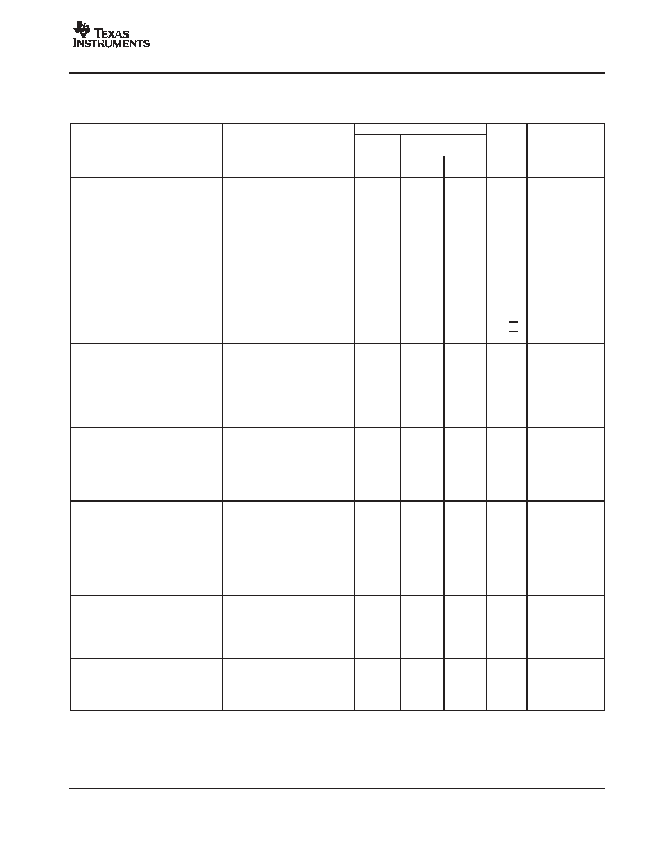
ELECTRICAL CHARACTERISTICS: V
S
= +5V
Boldface limits are tested at +25
∞
C.
At TA = 25
∞
C, G = +2, RF = 750
, and RL = 150
to VS/2, unless otherwise noted (see Figure 1).
OPA830ID, IDBV
TYP
MIN/MAX OVER TEMPERATURE
TEST
PARAMETER
CONDITIONS
+25
∞
C
+25
∞
C
(1)
0
∞
C to
70
∞
C
(2)
-40
∞
C to
+85
∞
C
(2)
UNITS
MIN/
MAX
TEST
LEVEL
(3)
AC PERFORMANCE (see Figure 1)
Small-Signal Bandwidth
G = +1, V
O
0.2V
PP
250
MHz
typ
C
G = +2, V
O
0.2V
PP
110
72
70
68
MHz
min
B
G = +5, V
O
0.2V
PP
24
17
16
15
MHz
min
B
G = +10, V
O
0.2V
PP
11
8
7
6
MHz
min
B
Gain-Bandwidth Product
G
+10
110
84
80
79
MHz
min
B
Peaking at a Gain of +1
V
O
0.2V
PP
5
dB
typ
C
Slew Rate
G = +2, 2V Step
550
280
270
260
V/
µ
s
min
B
Rise Time
0.5V Step
3.3
5.7
5.8
5.9
ns
max
B
Fall Time
0.5V Step
3.3
5.7
5.8
5.9
ns
max
B
Settling Time to 0.1%
G = +2, 1V Step
43
64
66
67
ns
max
B
Harmonic Distortion
V
O
= 2V
PP
, f = 5MHz
2nd-Harmonic
R
L
= 150
-62
-55
-54
-53
dBc
max
B
R
L
500
-64
-58
-57
-56
dBc
max
B
3rd-Harmonic
R
L
= 150
-58
-50
-49
-48
dBc
max
B
R
L
500
-84
-66
-63
-60
dBc
max
B
Input Voltage Noise
f > 1MHz
9.2
10.2
10.7
11.2
nV/
Hz
max
B
Input Current Noise
f > 1MHz
3.5
4.5
5.0
5.5
pA/
Hz
max
B
NTSC Differential Gain
0.08
%
typ
C
NTSC Differential Phase
0.09
∞
typ
C
DC PERFORMANCE
(4)
R
L
= 150
Open-Loop Voltage Gain
72
66
65
64
dB
min
A
Input Offset Voltage
±
0.5
±
5.0
±
6.0
±
6.5
mV
max
A
Average Offset Voltage Drift
--
±
20
±
20
µ
V/
∞
C
max
B
Input Bias Current
V
CM
= 2.5V
+5
+10
+12
+13
µ
A
max
A
Input Bias Current Drift
±
12
±
12
nA/
∞
C
max
B
Input Offset Current
V
CM
= 2.5V
±
0.1
±
0.8
±
1
±
1.2
µ
A
max
A
Input Offset Current Drift
--
±
5
±
5
nA/
∞
C
max
B
INPUT
Least Positive Input Voltage
(5)
-0.5
-0.4
-0.3
-0.2
V
max
A
Most Positive Input Voltage
(5)
3.2
3.1
3.0
2.9
V
min
A
Common-Mode Rejection Ratio (CMRR)
Input-Referred
80
76
74
72
dB
min
A
Input Impedance
Differential-Mode
10
2.1
k
pF
typ
C
Common-Mode
400
1.2
k
pF
typ
C
OUTPUT
Least Positive Output Voltage
G = +5, R
L
= 1k
to 2.5V
0.09
0.11
0.12
0.13
V
max
A
G = +5, R
L
= 150
to 2.5V
0.21
0.24
0.25
0.26
V
max
A
Most Positive Output Voltage
G = +5, R
L
= 1k
to 2.5V
4.91
4.89
4.88
4.87
V
min
A
G = +5, R
L
= 150
to 2.5V
4.78
4.75
4.73
4.72
V
min
A
Current Output, Sourcing and Sinking
±
80
±
60
±
55
±
52
mA
min
A
Short-Circuit Output Current
Output Shorted to Either Supply
140
mA
typ
C
Closed-Loop Output Impedance
G = +2, f
100kHz
0.06
typ
C
POWER SUPPLY
Minimum Operating Voltage
+2.8
V
typ
C
Maximum Operating Voltage
+11
+11
+11
V
max
A
Maximum Quiescent Current
V
S
= +5V
3.9
4.1
4.8
5.5
mA
max
A
Minimum Quiescent Current
V
S
= +5V
3.9
3.7
3.4
3.1
mA
min
A
Power-Supply Rejection Ratio (PSRR)
Input-Referred
66
61
60
59
dB
min
A
THERMAL CHARACTERISTICS
Specification: ID, IDBV
-40 to +85
∞
C
typ
C
Thermal Resistance,
q
JA
D
SO-8
125
∞
C/W
typ
C
DBV
SOT23-5
150
∞
C/W
typ
C
(1)
Junction temperature = ambient for +25
∞
C specifications.
(2)
Junction temperature = ambient at low temperature limits; junction temperature = ambient +5
∞
C at high temperature limit for over temperature.
(3)
Test levels: (A) 100% tested at +25
∞
C. Over temperature limits by characterization and simulation. (B) Limits set by characterization and simulation. (C) Typical value only
for information.
(4)
Current considered positive out of pin.
(5)
Tested < 3dB below minimum specified CMRR at
±
CMIR limits.
OPA830
SBOS263B - AUGUST 2004 - REVISED JANUARY 2005
www.ti.com
5
ELECTRICAL CHARACTERISTICS: V
S
= +3V
Boldface limits are tested at +25
∞
C.
At TA = 25
∞
C, G = +2, and RL = 150
to VS/3, unless otherwise noted (see Figure 2).
OPA830ID, IDBV
TYP
MIN/MAX OVER
TEMPERATURE
TEST
PARAMETER
CONDITIONS
+25
∞
C
+25
∞
C(1)
0
∞
C to
70
∞
C(2)
UNITS
MIN/
MAX
TEST
LEVEL
(3)
AC PERFORMANCE (see Figure 2)
Small-Signal Bandwidth
G = +2, VO
0.2VPP
100
72
68
MHz
min
B
G = +5, VO
0.2VPP
22
17
16
MHz
min
B
G = +10, VO
0.2VPP
10
8
7
MHz
min
B
Gain-Bandwidth Product
G
+10
100
80
76
MHz
min
B
Slew Rate
1V Step
225
140
110
V/
µ
s
min
B
Rise Time
0.5V Step
3.3
5.5
5.6
ns
max
B
Fall Time
0.5V Step
3.3
5.5
5.6
ns
max
B
Settling Time to 0.1%
1V Step
45
72
87
ns
max
B
Harmonic Distortion
VO = 1VPP, f = 5MHz
2nd-Harmonic
RL = 150
-67
-61
-59
dBc
max
B
RL
500
-67
-61
-59
dBc
max
B
3rd-Harmonic
RL = 150
-66
-59
-58
dBc
max
B
RL
500
-77
-59
-58
dBc
max
B
Input Voltage Noise
f > 1MHz
9.2
10.2
10.7
nV/
Hz
max
B
Input Current Noise
f > 1MHz
3.5
4.5
5.0
pA/
Hz
max
B
DC PERFORMANCE(4)
Open-Loop Voltage Gain
72
66
65
dB
min
A
Input Offset Voltage
±
1.5
±
7
±
8.1
mV
max
A
Average Offset Voltage Drift
--
±
25
µ
V/
∞
C
max
B
Input Bias Current
VCM = 1.0V
+5
+10
+12
µ
A
max
A
Input Bias Current Drift
±
12
nA/
∞
C
max
B
Input Offset Current
VCM = 1.0V
±
0.1
±
1
±
1.2
µ
A
max
A
Input Offset Current Drift
--
±
5
nA/
∞
C
max
B
INPUT
Least Positive Input Voltage(5)
-0.45
-0.4
-0.27
V
max
A
Most Positive Input Voltage(5)
1.2
1.1
1.0
V
min
A
Common-Mode Rejection Ratio (CMRR)
Input-Referred
80
75
73
dB
min
A
Input Impedance
Differential-Mode
10
2.1
k
pF
typ
C
Common-Mode
400
1.2
k
pF
typ
C
OUTPUT
Least Positive Output Voltage
G = +5, RL = 1k
to 1.5V
0.08
0.11
0.125
V
max
A
G = +5, RL = 150
to 1.5V
0.17
0.39
0.40
V
max
A
Most Positive Output Voltage
G = +5, RL = 1k
to 1.5V
2.91
2.88
2.85
V
min
A
G = +5, RL = 150
to 1.5V
2.82
2.74
2.70
V
min
A
Current Output, Sourcing
30
20
18
mA
min
A
Current Output, Sinking
30
20
18
mA
min
A
Short-Circuit Output Current
Output Shorted to Either Supply
45
mA
typ
C
Closed-Loop Output Impedance
See Figure 2, f < 100kHz
0.06
typ
C
POWER SUPPLY
Minimum Operating Voltage
+2.8
V
min
B
Maximum Operating Voltage
+11
+11
V
max
A
Maximum Quiescent Current
VS = +3V
3.7
4.0
4.7
mA
max
A
Minimum Quiescent Current
VS = +3V
3.7
3.3
3.1
mA
min
A
Power-Supply Rejection Ratio (PSRR)
Input-Referred
64
60
58
dB
min
A
THERMAL CHARACTERISTICS
Specification: ID, IDBV
-40 to +85
∞
C
typ
C
Thermal Resistance,
q
JA
D
SO-8
125
∞
C/W
typ
C
DBV
SOT23-5
150
∞
C/W
typ
C
(1)
Junction temperature = ambient for +25
∞
C specifications.
(2)
Junction temperature = ambient at low temperature limits; junction temperature = ambient +5
∞
C at high temperature limit for over temperature.
(3)
Test levels: (A) 100% tested at +25
∞
C. Over temperature limits by characterization and simulation. (B) Limits set by characterization and simulation. (C) Typical value only
for information.
(4) Current considered positive out of pin.
(5) Tested < 3dB below minimum specified CMRR at
±
CMIR limits.
OPA830
SBOS263B - AUGUST 2004 - REVISED JANUARY 2005
www.ti.com
6
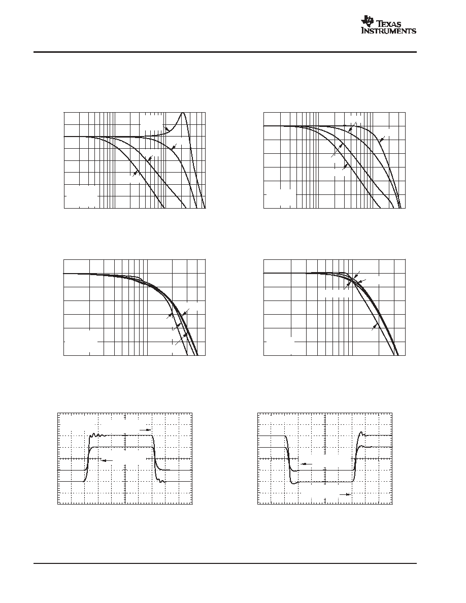
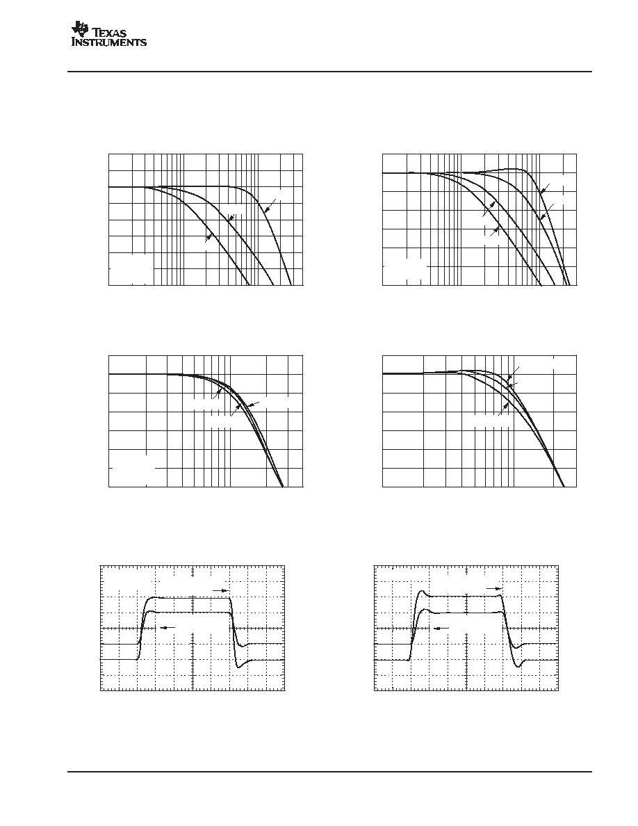
TYPICAL CHARACTERISTICS: V
S
=
±
5V
At TA = 25
∞
C, G = +2, RF = 750
, and RL = 150
to GND, unless otherwise noted (see Figure 3).
6
3
0
-
3
-
6
-
9
-
12
-
15
-
18
NONINVERTING SMALL-SIGNAL FREQUENCY RESPONSE
Frequency (MHz)
N
o
r
m
a
liz
e
d
G
a
in
(
d
B
)
1
10
100
600
V
O
= 0.2V
PP
R
L
= 150
See Figure 3
G = +1
R
F
= 0
G = +2
G = +5
G = +10
9
6
3
0
-
3
-
6
-
9
-
12
NONINVERTING LARGE-SIGNAL FREQUENCY RESPONSE
Frequency (MHz)
Ga
i
n
(d
B
)
10
100
500
V
O
= 4V
PP
V
O
= 2V
PP
V
O
= 1V
PP
V
O
= 0.5V
PP
G = +2V/V
R
L
= 150
See Figure 3
0.4
0.3
0.2
0.1
0
-
0.1
-
0.2
-
0.3
-
0.4
NONINVERTING PULSE RESPONSE
Time (10ns/div)
S
m
al
l
-
S
i
g
nal
O
u
t
p
ut
V
o
l
t
a
g
e
(
100m
V
/
di
v
)
2.0
1.5
1.0
0.5
0
-
0.5
-
1.0
-
1.5
-
2.0
L
a
r
ge-
S
i
gna
l
O
ut
put
V
o
l
t
a
g
e
(
50
0
m
V
/
di
v
)
Large-Signal
±
1V
Right Scale
Small-Signal
±
100mV
Left Scale
G = +2V/V
See Figure 3
3
0
-
3
-
6
-
9
-
12
-
15
-
18
INVERTING SMALL-SIGNAL FREQUENCY RESPONSE
Frequency (MHz)
N
o
r
m
a
liz
e
d
G
a
in
(
d
B
)
1
10
100
400
V
O
= 0.2V
PP
R
L
= 150
G =
-
2
G =
-
10
G =
-
1
G =
-
5
3
0
-
3
-
6
-
9
-
12
-
15
-
18
INVERTING LARGE-SIGNAL FREQUENCY RESPONSE
Frequency (MHz)
Ga
i
n
(d
B
)
10
100
400
G =
-
1V/V
R
L
= 150
V
O
= 2V
PP
V
O
= 4V
PP
V
O
= 1V
PP
V
O
= 0.5V
PP
0.4
0.3
0.2
0.1
0
-
0.1
-
0.2
-
0.3
-
0.4
INVERTING PULSE RESPONSE
Time (10ns/div)
S
m
al
l
-
S
i
g
nal
O
u
t
p
ut
V
o
l
t
a
g
e
(
100m
V
/
di
v
)
2.0
1.5
1.0
0.5
0
-
0.5
-
1.0
-
1.5
-
2.0
L
a
r
ge-
S
i
gna
l
O
ut
put
V
o
l
t
a
g
e
(
50
0
m
V
/
di
v
)
Large-Signal
±
1V
Right Scale
Small-Signal
±
100mV
Left Scale
G =
-
1V/V
OPA830
SBOS263B - AUGUST 2004 - REVISED JANUARY 2005
www.ti.com
7
TYPICAL CHARACTERISTICS: V
S
=
±
5V (continued)
At TA = 25
∞
C, G = +2, RF = 750
, and RL = 150
to GND, unless otherwise noted (see Figure 3).
-
50
-
55
-
60
-
65
-
70
-
75
-
80
-
85
HARMONIC DISTORTION vs LOAD RESISTANCE
Resistance (
)
H
a
r
m
o
n
i
c
D
is
t
o
r
t
io
n
(
d
B
c)
100
1000
f = 5MHz
V
O
= 2V
PP
G = +2V/V
See Figure 3
3rd-Harmonic
2nd-Harmonic
-
55
-
60
-
65
-
70
-
75
-
80
-
85
-
90
-
95
HARMONIC DISTORTION vs OUTPUT VOLTAGE
Output Voltage Swing (V
PP
)
H
a
r
m
oni
c
D
i
s
tor
t
i
o
n
(
dB
c
)
0.1
1
10
2nd-Harmonic
3rd-Harmonic
f = 5MHz
R
L
= 500
G = +2V/V
See Figure 3
-
40
-
45
-
50
-
55
-
60
-
65
-
70
-
75
-
80
-
85
-
90
TWO-TONE, 3RD-ORDER INTERMODULATION SPURIOUS
Single-Tone Load Power (2dBm/div)
3r
d-
O
r
der
S
p
ur
i
o
u
s
L
e
v
e
l
(
dB
c
)
-
26
-
20
-
14
-
8
-
2
6
10MHz
5MHz
20MHz
750
OPA830
P
I
P
O
50
500
750
-
40
-
45
-
50
-
55
-
60
-
65
-
70
-
75
-
80
-
85
-
90
5MHz HARMONIC DISTORTION vs SUPPLY VOLTAGE
Supply Voltage (
±
V
S
)
Ha
r
m
o
n
i
c
Di
s
t
o
r
ti
o
n
(
d
B
c
)
2.0
2.5
3.0
3.5
4.0
4.5
5.0
5.5
V
O
= 2V
PP
R
L
= 500
G = +2V/V
See Figure 3
2nd-Harmonic
3rd-Harmonic
Input Limited for V
CM
= 0V
-
50
-
55
-
60
-
65
-
70
-
75
-
80
-
85
-
90
-
95
-
100
-
105
HARMONIC DISTORTION vs FREQUENCY
Frequency (MHz)
H
a
r
m
oni
c
D
i
s
tor
t
i
o
n
(
dB
c
)
0.1
1
10
3rd-Harmonic
R
L
= 150
2nd-Harmonic
R
L
= 150
2nd-Harmonic
R
L
= 500
3rd-Harmonic
R
L
= 500
V
O
= 2V
PP
G = +2V/V
See Figure 3
95
90
85
80
75
50
25
SUPPLY AND OUTPUT CURRENT vs TEMPERATURE
Ambient Temperature (
_
C)
O
u
tp
u
t
C
u
r
r
ent
(
50mA
/
d
i
v
)
6.0
5.5
5.0
4.5
4.0
3.5
3.0
Su
p
p
ly
C
u
r
r
e
n
t
(
4
m
A
/
d
iv
)
-
50
-
25
0
25
50
75
100
125
Source/Sink Output Current
Left Scale
Supply Current
Right Scale

OPA830
SBOS263B - AUGUST 2004 - REVISED JANUARY 2005
www.ti.com
8
TYPICAL CHARACTERISTICS: V
S
=
±
5V (continued)
At TA = 25
∞
C, G = +2, RF = 750
, and RL = 150
to GND, unless otherwise noted (see Figure 3).
8
7
6
5
4
3
2
1
0
-
1
-
2
-
3
FREQUENCY RESPONSE vs CAPACITIVE LOAD
Frequency (MHz)
N
o
r
m
a
l
i
z
ed
G
a
i
n
to
C
a
pa
c
i
t
i
v
e
Lo
a
d
(
d
B
)
1
10
100
200
C
L
= 1000pF
C
L
= 100pF
C
L
= 10pF
750
R
S
OPA830
V
I
V
O
50
1k
(1)
C
L
750
NOTE: (1) 1k
is optional.
6
5
4
3
2
1
0
-
1
-
2
-
3
-
4
-
5
-
6
OUTPUT SWING vs LOAD RESISTANCE
Resistance (
)
O
u
t
put
V
o
l
t
age
(
V
)
10
100
1k
G = +5V/V
V
S
=
±
5V
120
110
100
90
80
70
60
50
40
30
20
10
RECOMMENDED R
S
vs CAPACITIVE LOAD
Capacitive Load (pF)
R
S
(
)
1
10
100
1k
0dB Peaking Targeted
6
5
4
3
2
1
0
-
1
-
2
-
3
-
4
-
5
-
6
OUTPUT VOLTAGE AND CURRENT LIMITATIONS
I
O
(mA)
V
O
(V
)
-
160
-
120
-
80
-
40
0
40
80
120
160
1W Internal
Power Lim it
Output
Current Limit
Output
Current Lim it
1W Internal
P ower Limit
R
L
= 500
R
L
= 100
R
L
= 50
OPA830
SBOS263B - AUGUST 2004 - REVISED JANUARY 2005
www.ti.com
9
TYPICAL CHARACTERISTICS: V
S
=
±
5V, Differential Configuration
At TA = 25
∞
C, GD = +2, RF = 604
, and RL = 500
, unless otherwise noted.
R
L
50 0
6 0 4
6 0 4
R
G
R
G
V
O
V
I
G
D
=
604
R
G
+5V
-
5V
-
5V
+5V
OPA830
OPA830
9
6
3
0
-
3
-
6
-
9
DIFFERENTIAL LARGE-SIGNAL FREQUENCY RESPONSE
Frequency (MHz)
1
10
200
100
Ga
i
n
(d
B
)
V
O
= 5V
PP
V
O
= 2V
PP
V
O
= 1V
PP
V
O
= 200mV
PP
G
D
= 2
R
L
= 500
-
40
-
50
-
60
-
70
-
80
-
90
-
100
-
110
DIFFERENTIAL DISTORTION vs FREQUENCY
Frequency (MHz)
0.1
1
10
100
Ha
r
m
o
n
i
c
Di
s
t
o
r
ti
o
n
(
d
B
c
)
3rd-Harmonic
2nd-Harmonic
G
D
= 2
V
O
= 4V
PP
R
L
= 500
3
0
-
3
-
6
-
9
-
12
-
15
DIFFERENTIAL SMALL-SIGNAL FREQUENCY RESPONSE
Frequency (MHz)
1
10
100
200
N
o
r
m
a
l
iz
e
d
G
a
in
(
d
B
)
G
D
= 1
G
D
= 2
G
D
= 5
G
D
= 10
V
O
= 200mV
PP
R
L
= 500
-
45
-
50
-
55
-
60
-
65
-
70
-
75
-
80
-
85
-
90
-
95
-
100
DIFFERENTIAL DISTORTION vs LOAD RESISTANCE
Resistance (
)
100
150
200
250
300
350
400
450
500
Ha
r
m
o
n
i
c
Di
s
t
o
r
t
i
o
n
(
d
B
c
)
3rd-Harmonic
2nd-Harmonic
V
O
= 4V
PP
G
D
= 2
f = 5MHz
-
55
-
60
-
65
-
70
-
75
-
80
-
85
-
90
-
95
-
100
-
105
DIFFERENTIAL DISTORTION vs OUTPUT VOLTAGE
Output Voltage Swing (V
PP
)
1
10
Ha
r
m
o
n
i
c
Di
s
t
r
t
i
o
n
(
d
B
c
)
3rd-Harmonic
2nd-Harmonic
G
D
= 2
R
L
= 500
f = 5MHz

OPA830
SBOS263B - AUGUST 2004 - REVISED JANUARY 2005
www.ti.com
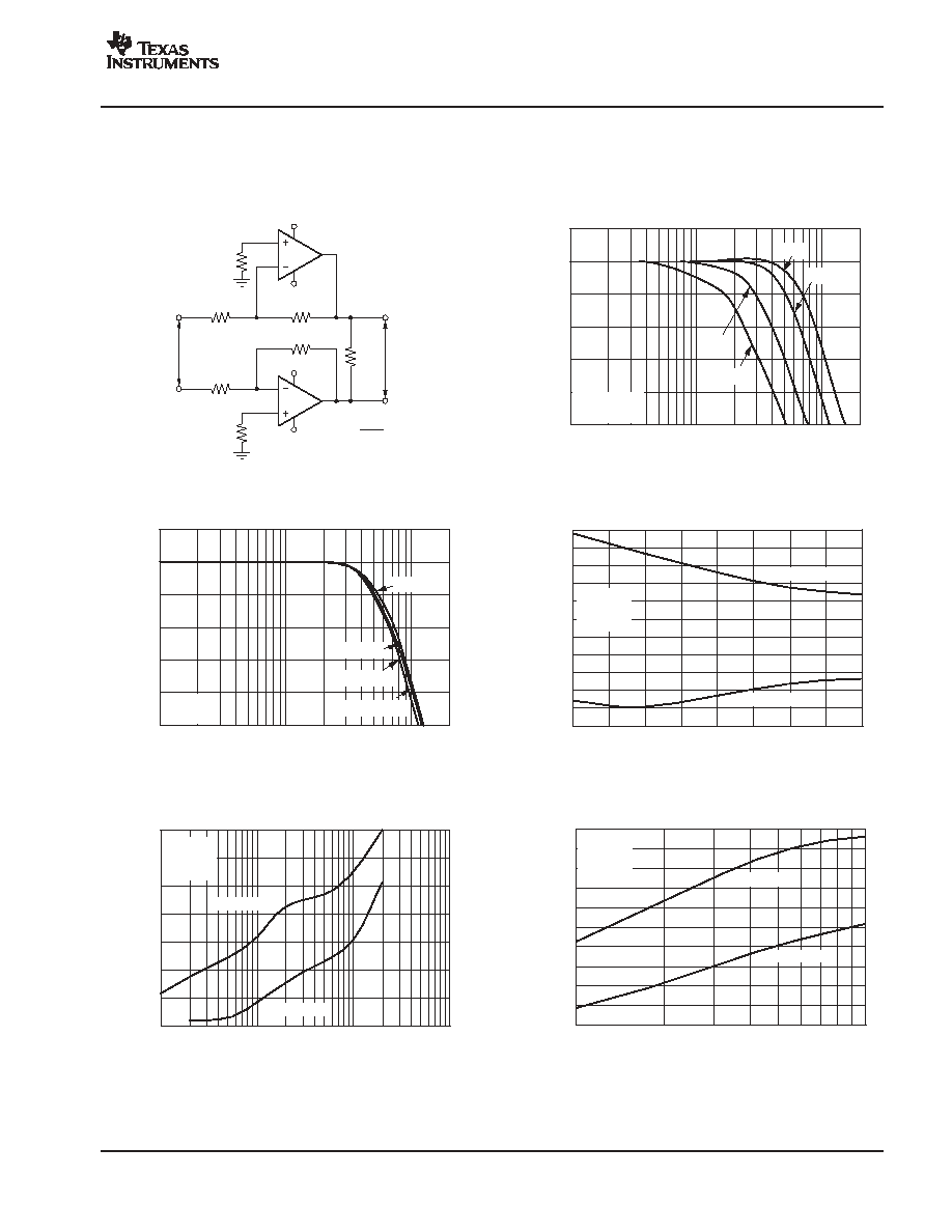
10
TYPICAL CHARACTERISTICS: V
S
= +5V
At TA = 25
∞
C, G = +2, RF = 750
, RL = 150
to VS/2, and input VCM = 2.5V, unless otherwise noted (see Figure 1).
6
3
0
-
3
-
6
-
9
-
12
-
15
-
18
NONINVERTING SMALL-SIGNAL FREQUENCY RESPONSE
Frequency (MHz)
N
o
r
m
a
liz
e
d
G
a
in
(
d
B
)
1
10
100
500
V
O
= 0.2V
PP
R
L
= 150
See Figure 1
G = +1
R
F
= 0
G = +2
G = +5
G = +10
9
6
3
0
-
3
-
6
-
9
-
12
NONINVERTING LARGE-SIGNAL FREQUENCY RESPONSE
Frequency (MHz)
Ga
i
n
(d
B
)
10
100
500
G = +2V/V
R
L
= 150
See Figure 1
V
O
= 2V
PP
V
O
= 1V
PP
V
O
= 0.5V
PP
2.9
2.8
2.7
2.6
2.5
2.4
2.3
2.2
2.1
NONINVERTING PULSE RESPONSE
Time (10ns/div)
S
m
a
l
l
-
S
i
gna
l
O
utp
u
t
V
ol
ta
ge
(
100mV
/
di
v
)
4.5
4.0
3.5
3.0
2.5
2.0
1.5
1.0
0.5
L
a
r
g
e
-
S
i
gnal
O
u
t
p
u
t
V
o
l
t
age
(
5
0
0
mV
/
d
i
v
)
Large-Signal
±
1V
Right Scale
Small-Signal
±
100mV
Left Scale
G = +2V/V
See Figure 1
3
0
-
3
-
6
-
9
-
12
-
15
-
18
INVERTING SMALL-SIGNAL FREQUENCY RESPONSE
Frequency (MHz)
N
o
r
m
a
liz
e
d
G
a
in
(
d
B
)
1
10
100
400
V
O
= 0.2V
PP
R
L
= 150
See Figure 9
G =
-
2
G =
-
10
G =
-
1
G =
-
5
3
0
-
3
-
6
-
9
-
12
-
15
-
18
INVERTING LARGE-SIGNAL FREQUENCY RESPONSE
Frequency (MHz)
Ga
i
n
(d
B
)
10
100
500
G =
-
1V/V
R
L
= 150
See Figure 9
V
O
= 2V
PP
V
O
= 1V
PP
V
O
= 0.5V
PP
2.9
2.8
2.7
2.6
2.5
2.4
2.3
2.2
2.1
INVERTING PULSE RESPONSE
Time (10ns/div)
S
m
a
l
l
-
S
i
gna
l
O
utp
u
t
V
ol
ta
ge
(
100mV
/
di
v
)
4.5
4.0
3.5
3.0
2.5
2.0
1.5
1.0
0.5
L
a
r
g
e
-
S
i
gnal
O
u
t
p
u
t
V
o
l
t
age
(
5
0
0
mV
/
d
i
v
)
Large-Signal
±
1V
Right Scale
Small-Signal
±
100mV
Left Scale
G =
-
1V/V

OPA830
SBOS263B - AUGUST 2004 - REVISED JANUARY 2005
www.ti.com
11
TYPICAL CHARACTERISTICS: V
S
= +5V (continued)
At TA = 25
∞
C, G = +2, RF = 750
, RL = 150
to VS/2, and input VCM = 2.5V, unless otherwise noted (see Figure 1).
-
50
-
55
-
60
-
65
-
70
-
75
-
80
-
85
-
90
HARMONIC DISTORTION vs LOAD RESISTANCE
Load Resistance (
)
H
a
r
m
o
n
i
c
D
is
t
o
r
t
io
n
(
d
B
c)
100
1000
f = 5MHz
V
O
= 2V
PP
G = +2V/V
See Figure 1
3rd-Harmonic
2nd-Harmonic
-
45
-
50
-
55
-
60
-
65
-
70
-
75
-
80
-
85
-
90
-
95
-
100
HARMONIC DISTORTION vs OUTPUT VOLTAGE
Output Voltage Swing (V
PP
)
H
a
r
m
oni
c
D
i
s
tor
t
i
o
n
(
dB
c
)
0.1
1
10
2nd-Harmonic
3rd-Harmonic
f = 5MHz
R
L
= 500
G = +2V/V
See Figure 1
Input Limited
-
55
-
60
-
65
-
70
-
75
-
80
-
85
HARMONIC DISTORTION vs INVERTING GAIN
Gain (
V/V
)
H
a
r
m
o
n
i
c
D
is
t
o
r
t
io
n
(
d
B
c)
1
10
f = 5MHz
R
L
= 500
V
O
= 2V
PP
3rd-Harmonic
2nd-Harmonic
-
50
-
55
-
60
-
65
-
70
-
75
-
80
-
85
-
90
-
95
-
100
-
105
HARMONIC DISTORTION vs FREQUENCY
Frequency (MHz)
H
a
r
m
oni
c
D
i
s
tor
t
i
o
n
(
dB
c
)
0.1
1
10
3rd-Harmonic
R
L
= 150
2nd-Harmonic
R
L
= 150
2nd-Harmonic
R
L
= 500
3rd-Harmonic
R
L
= 500
G = +2V/V
V
O
= 2V
PP
See Figure 1
-
55
-
60
-
65
-
70
-
75
-
80
-
85
-
90
HARMONIC DISTORTION vs NONINVERTING GAIN
Gain (V/V)
H
a
r
m
oni
c
D
i
s
tor
t
i
o
n
(
dB
c
)
1
10
f = 5MHz
R
L
= 500
V
O
= 2V
PP
See Figure 1
3rd-Harmonic
2nd-Harmonic
-
45
-
50
-
55
-
60
-
65
-
70
-
75
-
80
-
85
-
90
-
95
TWO-TONE, 3RD-ORDER INTERMODULATION SPURIOUS
Single-Tone Load Power (dBm)
3r
d-
O
r
der
S
p
u
r
i
ous
Le
v
e
l
(
d
B
c
)
10MHz
5MHz
20MHz
750
OPA830
P
I
P
O
50
500
750
-
26
-
24
-
22
-
20
-
18
-
16
-
14
-
12
-
10
-
8
-
6
-
4
-
2

OPA830
SBOS263B - AUGUST 2004 - REVISED JANUARY 2005
www.ti.com
12
TYPICAL CHARACTERISTICS: V
S
= +5V (continued)
At TA = 25
∞
C, G = +2, RF = 750
, RL = 150
to VS/2, and input VCM = 2.5V, unless otherwise noted (see Figure 1).
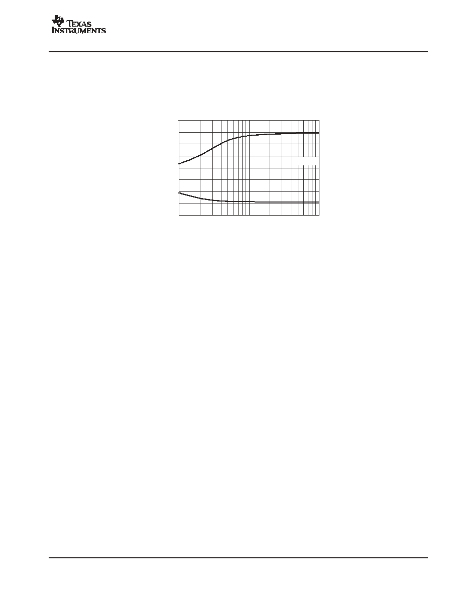
100
10
1
INPUT VOLTAGE AND CURRENT NOISE DENSITY
Frequency (Hz)
10
100
1k
10k
100k
1M
10M
Vo
lt
a
g
e
N
o
i
se
(
n
V/
Hz
)
Cu
r
r
e
n
t
N
o
i
s
e
(
p
A
/
Hz
)
Voltage Noise
(9.2nV/
Hz)
Current Noise
(3.5pA/
Hz)
130
120
110
100
90
80
70
60
50
40
30
20
10
RECOMMENDED R
S
vs CAPACITIVE LOAD
Capacitive Load (pF)
R
S
(
)
1
10
100
1k
0dB Peaking Targeted
80
70
60
50
40
30
20
10
0
-
10
-
20
OPEN-LOOP GAIN AND PHASE
Frequency (Hz)
O
p
e
n
-
L
oo
p
G
ai
n
(
d
B
)
180
160
140
120
100
80
60
40
20
0
-
20
O
p
e
n
-
L
oo
p
G
ai
n
(
d
B
)
100
1k
10k
100k
1M
10M
100M
1G
20 log (A
OL
)
(A
OL
)
100
10
1
0.1
0.01
CLOSED-LOOP OUTPUT IMPEDANCE vs FREQUENCY
Frequency (Hz)
O
u
tput
Imped
anc
e
(
)
1k
10k
100k
1M
10M
100M
8
7
6
5
4
3
2
1
0
-
1
-
2
-
3
FREQUENCY RESPONSE vs CAPACITIVE LOAD
Frequency (MHz)
N
o
r
m
al
i
z
e
d
G
a
i
n
t
o
C
a
p
a
c
i
ti
v
e
Load
(
d
B
)
1
10
100
300
C
L
= 1000pF
C
L
= 100pF
C
L
= 10pF
750
R
S
O P A830
V
I
V
O
50
1k
(1)
C
L
750
NOTE: (1) 1k
is optional.
5.0
4.5
4.0
3.5
3.0
2.5
2.0
1.5
1.0
0.5
0
-
0.5
-
1.0
VOLTAGE RANGES vs TEMPERATURE
Ambient Temperature (10
_
C/div)
-
50
0
50
110
V
o
l
t
a
g
e
R
an
ge
(
V
)
Most Positive Output Voltage
Most Positive Input Voltage
Least Positive Output Voltage
Least Positive Input Voltage
R
L
= 150

OPA830
SBOS263B - AUGUST 2004 - REVISED JANUARY 2005
www.ti.com
13
TYPICAL CHARACTERISTICS: V
S
= +5V (continued)
At TA = 25
∞
C, G = +2, RF = 750
, RL = 150
to VS/2, and input VCM = 2.5V, unless otherwise noted (see Figure 1).
4
3
2
1
0
-
1
-
2
-
3
-
8
TYPICAL DC DRIFT OVER TEMPERATURE
Ambient Temperature (
_
C)
In
pu
t
O
f
f
s
e
t
V
o
l
t
ag
e
(
m
V
)
8
6
4
2
0
-
2
-
4
-
6
-
8
I
n
p
u
t
B
i
a
s
and
O
f
f
s
et
C
u
r
r
ent
(
µ
V)
-
50
-
25
0
25
50
75
100
125
Input Bias Current (I
B
)
10
◊
Input Offset Current (I
OS
)
Input Offset Voltage (V
OS
)
90
80
70
60
50
40
30
20
10
0
CMRR AND PSRR vs FREQUENCY
Frequency (Hz)
Co
m
m
o
n
-
M
o
d
e
Re
j
e
c
t
i
o
n
R
a
t
i
o
(
d
B
)
Po
w
e
r
-
S
u
p
p
ly
R
e
je
ct
io
n
R
a
t
i
o
(
d
B)
1k
10k
100k
1M
10M
100M
CMRR
PSRR
100
95
90
85
80
75
70
65
60
SUPPLY AND OUTPUT CURRENT vs TEMPERATURE
Ambient Temperature (
_
C)
O
u
tput
C
u
r
r
ent
(
5
m
A
/di
v
)
6.0
5.5
5.0
4.5
4.0
3.5
3.0
2.5
2.0
S
u
ppl
y
C
u
r
r
ent
(
0
.
5
mA
/di
v
)
-
50
-
25
0
25
50
75
100
125
Output Current, Sinking
Quiescent Current
Output Current, Sourcing
5.5
5.0
4.5
4.0
3.5
3.0
2.5
2.0
1.5
1.0
0.5
0
-
0.5
OUTPUT SWING vs LOAD RESISTANCE
Load Resistance (
)
O
u
t
put
V
o
l
t
age
(
V
)
10
100
1k
G = +5V/V
OPA830
SBOS263B - AUGUST 2004 - REVISED JANUARY 2005
www.ti.com
14
TYPICAL CHARACTERISTICS: V
S
= +5V, Differential Configuration
At TA = 25
∞
C, G = +2, RF = 604
, and RL = 500
differential, unless otherwise noted.
R
L
60 4
60 4
R
G
R
G
V
O
V
I
G
D
=
604
R
G
+5V
+5V
OPA830
OPA830
1.2k
1.2k
1.2k
0.1
µ
F
1.2k
0.1
µ
F
2.5V
2.5V
9
6
3
0
-
3
-
6
-
9
DIFFERENTIAL LARGE-SIGNAL FREQUENCY RESPONSE
Frequency (MHz)
1
10
100
200
Ga
i
n
(d
B
)
V
O
= 3V
PP
V
O
= 2V
PP
V
O
= 1V
PP
V
O
= 0.2V
PP
G
D
= 2
R
L
= 500
-
30
-
40
-
50
-
60
-
70
-
80
-
90
-
100
-
110
DIFFERENTIAL DISTORTION vs FREQUENCY
Frequency (MHz)
1
10
100
Ha
r
m
o
n
i
c
Di
s
t
r
t
i
o
n
(
d
B
c
)
3rd-Harmonic
2nd-Harmonic
V
O
= 4V
PP
G
D
= 2
R
L
= 500
3
0
-
3
-
6
-
9
-
12
-
15
DIFFERENTIAL SMALL-SIGNAL FREQUENCY RESPONSE
Frequency (MHz)
1
10
100
200
N
o
r
m
a
l
iz
e
d
G
a
in
(
d
B
)
G
D
= 1
G
D
= 2
G
D
= 5
G
D
= 10
V
O
= 200mV
PP
R
L
= 500
-
40
-
45
-
50
-
55
-
60
-
65
-
70
-
75
-
80
-
85
-
90
DIFFERENTIAL DISTORTION vs LOAD RESISTANCE
Resistance (
)
100
150
200
250
300
350
400
450
500
Ha
r
m
o
n
i
c
Di
s
t
o
r
t
i
o
n
(
d
B
c
)
3rd-Harmonic
2nd-Harmonic
V
O
= 4V
PP
G
D
= 2
f = 5MHz
-
55
-
60
-
65
-
70
-
75
-
80
-
85
-
90
-
95
-
100
DIFFERENTIAL DISTORTION vs OUTPUT VOLTAGE
Output Voltage Swing (V
PP
)
1
10
Ha
r
m
o
n
i
c
Di
s
t
r
t
i
o
n
(
d
B
c
)
3rd-Harmonic
2nd-Harmonic
G
D
= 2
R
L
= 500
f = 5MHz
OPA830
SBOS263B - AUGUST 2004 - REVISED JANUARY 2005
www.ti.com
15
TYPICAL CHARACTERISTICS: V
S
= +3V
At TA = 25
∞
C, G = +2, and RL = 150
to VS/3, unless otherwise noted (see Figure 2).
6
3
0
-
3
-
6
-
9
-
12
-
15
-
18
NONINVERTING SMALL-SIGNAL FREQUENCY RESPONSE
Frequency (MHz)
N
o
r
m
a
liz
e
d
G
a
in
(
d
B
)
1
10
100
400
R
L
= 150
V
O
= 0.2V
PP
See Figure 2
G = +2
G = +10
G = +5
9
6
3
0
-
3
-
6
-
9
-
12
NONINVERTING LARGE-SIGNAL FREQUENCY RESPONSE
Frequency (MHz)
Ga
i
n
(d
B
)
10
100
400
R
L
= 150
G = +2V/V
See Figure 2
V
O
= 1.5V
PP
V
O
= 1V
PP
V
O
= 0.5V
PP
1.20
1.15
1.10
1.05
1.00
0.95
0.90
0.85
0.80
NONINVERTING PULSE RESPONSE
Time (10ns/div)
S
m
al
l
-
S
i
g
nal
O
u
t
p
u
t
V
o
l
t
ag
e
(
90
mV
/
d
i
v
)
2.00
1.75
1.50
1.25
1.00
0.75
0.50
0.25
0
L
a
r
ge-
S
i
g
nal
O
u
t
put
V
o
l
t
a
g
e
(
25
0
m
V
/
di
v
)
Large-Signal
±
0.5V
Right Scale
Small-Signal
±
100mV
Left Scale
G = +2V/V
See Figure 2
3
0
-
3
-
6
-
9
-
12
-
15
-
18
INVERTING SMALL-SIGNAL FREQUENCY RESPONSE
Frequency (MHz)
N
o
r
m
a
liz
e
d
G
a
in
(
d
B
)
1
10
100
300
G =
-
10
G =
-
5
G =
-
2
G =
-
1
R
L
= 150
V
O
= 0.2V
PP
3
0
-
3
-
6
-
9
-
12
-
15
-
18
INVERTING LARGE-SIGNAL FREQUENCY RESPONSE
Frequency (MHz)
Ga
i
n
(d
B
)
10
100
300
R
L
= 150
G =
-
1V/V
V
O
= 1.5V
PP
V
O
= 1V
PP
V
O
= 0.5V
PP
1.20
1.15
1.10
1.05
1.00
0.95
0.90
0.85
0.80
INVERTING PULSE RESPONSE
Time (10ns/div)
S
m
al
l
-
S
i
g
nal
O
u
t
p
u
t
V
o
l
t
ag
e
(
90
mV
/
d
i
v
)
2.00
1.75
1.50
1.25
1.00
0.75
0.50
0.25
0
L
a
r
ge-
S
i
g
nal
O
u
t
put
V
o
l
t
a
g
e
(
25
0
m
V
/
di
v
)
Large-Signal
±
0.5V
Right Scale
Small-Signal
±
100mV
Left Scale
G =
-
1V/V

OPA830
SBOS263B - AUGUST 2004 - REVISED JANUARY 2005
www.ti.com
16
TYPICAL CHARACTERISTICS: V
S
= +3V (continued)
At TA = 25
∞
C, G = +2, and RL = 150
to VS/3, unless otherwise noted (see Figure 2).
-
50
-
55
-
60
-
65
-
70
-
75
-
80
-
85
-
90
HARMONIC DISTORTION vs LOAD RESISTANCE
Resistance (
)
H
a
r
m
o
n
i
c
D
is
t
o
r
t
io
n
(
d
B
c)
100
1000
f = 5MHz
V
O
= 1V
PP
G = +2V/V
See Figure 2
3rd-Harmonic
2nd-Harmonic
-
55
-
60
-
65
-
70
-
75
-
80
-
85
-
90
-
95
-
100
HARMONIC DISTORTION vs FREQUENCY
Frequency (MHz)
H
a
r
m
oni
c
D
i
s
tor
t
i
o
n
(
dB
c
)
0.1
1
10
2nd-Harmonic
R
L
= 150
2nd-Harmonic
R
L
= 500
3rd-Harmonic
R
L
= 150
3rd-Harmonic
R
L
= 500
V
O
= 1V
PP
G = +2V/V
See Figure 2
190
170
150
130
110
90
70
50
30
10
RECOMMENDED R
S
vs CAPACITIVE LOAD
Capacitive Load (pF)
R
S
(
)
1
10
100
1k
0dB Peaking Targeted
-
40
-
50
-
60
-
70
-
80
-
90
-
100
HARMONIC DISTORTION vs OUTPUT VOLTAGE
Output Voltage Swing (V
PP
)
H
a
r
m
o
n
i
c
D
is
t
o
r
t
io
n
(
d
B
c)
0.1
1
10
2nd-Harmonic
3rd-Harmonic
f = 5MHz
R
L
= 500
G = +2V/V
See Figure 2
Input Limited
-
40
-
45
-
50
-
55
-
60
-
65
-
70
-
75
-
80
-
85
-
90
-
95
TWO-TONE, 3RD-ORDER INTERMODULATION SPURIOUS
Single-Tone Load Power (dBm)
3r
d-
O
r
der
S
p
u
r
i
ous
Le
v
e
l
(
d
B
c
)
10MHz
5MHz
20MHz
-
28
-
26
-
24
-
22
-
20
-
18
-
16
-
14
-
12
-
10
-
8
750
OPA830
P
I
P
O
50
500
750
8
7
6
5
4
3
2
1
0
-
1
-
2
-
3
FREQUENCY RESPONSE vs CAPACITIVE LOAD
Frequency (MHz)
N
o
r
m
al
i
z
e
d
G
a
i
n
t
o
C
a
p
a
c
i
ti
v
e
Load
(
d
B
)
1
10
100
200
C
L
= 1000pF
C
L
= 100pF
C
L
= 10pF
750
R
S
V
I
V
O
50
1k
(1)
C
L
750
NOTE: (1) 1k
is optional.
O P A830
OPA830
SBOS263B - AUGUST 2004 - REVISED JANUARY 2005
www.ti.com
17
TYPICAL CHARACTERISTICS: V
S
= +3V (continued)
At TA = 25
∞
C, G = +2, and RL = 150
to VS/3, unless otherwise noted (see Figure 2).
3.5
3.0
2.5
2.0
1.5
1.0
0.5
0
-
0.5
OUTPUT SWING vs LOAD RESISTANCE
Load Resistance (
)
Ou
t
p
u
t
V
o
l
t
a
g
e
(
V
)
10
100
1k
G = +5V/V

OPA830
SBOS263B - AUGUST 2004 - REVISED JANUARY 2005
www.ti.com
18
TYPICAL CHARACTERISTICS: V
S
= +3V, Differential Configuration
At TA = 25
∞
C, G = +2, RF = 604
, and RL = 500
differential, unless otherwise noted.
R
L
6 0 4
6 0 4
R
G
R
G
V
O
V
I
G
D
=
604
R
G
+3V
2k
1k
0.1
µ
F
2k
1k
+3V
OPA 830
OPA 830
0.1
µ
F
1V
1V
9
6
3
0
-
3
-
6
-
9
DIFFERENTIAL LARGE-SIGNAL FREQUENCY RESPONSE
Frequency (MHz)
1
10
100
200
Ga
i
n
(d
B
)
V
O
= 2V
PP
V
O
= 1V
PP
V
O
= 200mV
PP
G
D
= 2
-
35
-
45
-
55
-
65
-
75
-
85
-
95
-
105
-
115
DIFFERENTIAL DISTORTION vs FREQUENCY
Frequency (MHz)
0.1
1
10
100
Ha
r
m
o
n
i
c
Di
s
t
o
r
ti
o
n
(
d
B
c
)
3rd-Harmonic
2nd-Harmonic
G
D
= 2
V
O
= 2V
PP
R
L
= 500
3
0
-
3
-
6
-
9
-
12
-
15
DIFFERENTIAL SMALL-SIGNAL FREQUENCY RESPONSE
Frequency (MHz)
1
10
100
200
N
o
r
m
a
l
iz
e
d
G
a
in
(
d
B
)
G
D
= 1
G
D
= 2
G
D
= 5
G
D
= 10
V
O
= 200mV
PP
R
L
= 500
-
40
-
45
-
50
-
55
-
60
-
65
-
70
-
75
-
80
-
85
-
90
DIFFERENTIAL DISTORTION vs LOAD RESISTANCE
Resistance (
)
100
150
200
250
300
350
400
450
500
Ha
r
m
o
n
i
c
Di
s
t
o
r
t
i
o
n
(
d
B
c
)
3rd-Harmonic
2nd-Harmonic
V
O
= 4V
PP
G
D
= 2
f = 5MHz
-
75
-
80
-
85
-
90
-
95
-
100
DIFFERENTIAL DISTORTION vs OUTPUT VOLTAGE
Output Voltage Swing (V
PP
)
0.50
0.75
1.00
1.25
1.50
1.75
2.00
Ha
r
m
o
n
i
c
Di
s
t
o
r
t
i
o
n
(
d
B
c
)
3rd-Harmonic
2nd-Harmonic
G
D
= 2
R
L
= 500
f = 5MHz

OPA830
SBOS263B - AUGUST 2004 - REVISED JANUARY 2005
www.ti.com
19
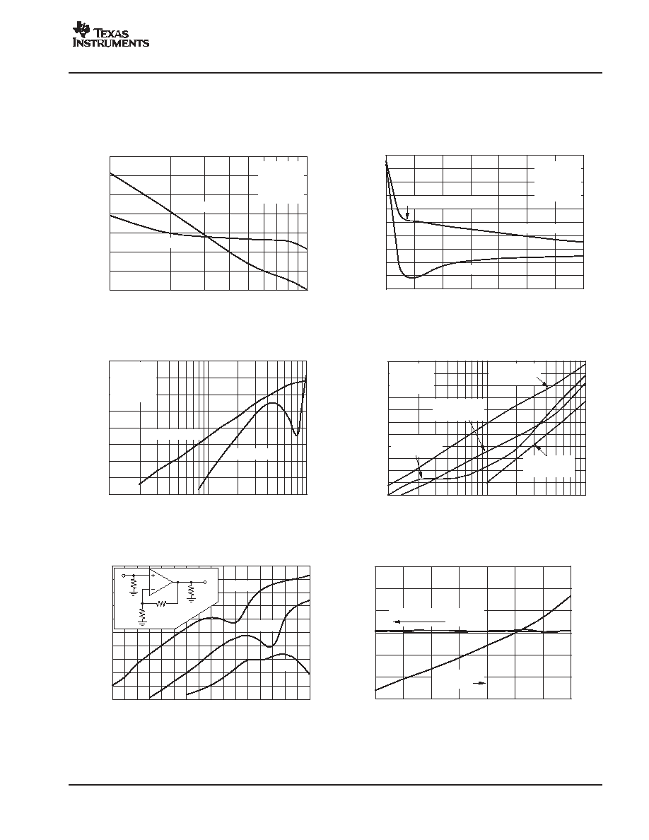
APPLICATIONS INFORMATION
WIDEBAND VOLTAGE-FEEDBACK
OPERATION
The OPA830 is a unity-gain stable, very high-speed
voltage-feedback op amp designed for single-supply
operation (+3V to +10V). The input stage supports input
voltages below ground and to within 1.7V of the positive
supply. The complementary common-emitter output stage
provides an output swing to within 25mV of ground and the
positive supply. The OPA830 is compensated to provide
stable operation with a wide range of resistive loads.
Figure 1 shows the AC-coupled, gain of +2 configuration
used for the +5V Specifications and Typical Characteristic
Curves. For test purposes, the input impedance is set to
50
with a resistor to ground. Voltage swings reported in
the Electrical Characteristics are taken directly at the input
and output pins. For the circuit of Figure 1, the total
effective load on the output at high frequencies is
150
|| 1500
. The 1.5k
resistors at the noninverting
input provide the common-mode bias voltage. Their
parallel combination equals the DC resistance at the
inverting input (R
F
), reducing the DC output offset due to
input bias current.
OPA830
V
S
= +5V
V
OUT
53.6
V
IN
1.50k
+V
S
/2
1.50k
R
L
150
+V
S
2
6.8
µ
F
+
0.1
µ
F
0.1
µ
F
R
F
750
R
G
750
2.5V
Figure 1. AC-Coupled, G = +2, +5V Single-Supply
Specification and Test Circuit
Figure 2 shows the AC-coupled, gain of +2 configuration
used for the +3V Specifications and Typical Characteristic
Curves. For test purposes, the input impedance is set to
50
with a resistor to ground. Voltage swings reported in
the Electrical Characteristics are taken directly at the input
and output pins. For the circuit of Figure 2, the total
effective load on the output at high frequencies is
150
|| 1500
. The 1.13k
and 2.26k
resistors at the
noninverting input provide the common-mode bias
voltage. Their parallel combination equals the DC
resistance at the inverting input (R
F
), reducing the DC
output offset due to input bias current.
OPA830
V
S
= +3V
V
OUT
53.6
V
IN
2.26k
1.13k
R
L
150
+V
S
3
6.8
µ
F
+
0.1
µ
F
0.1
µ
F
R
F
750
R
G
750
+1V
+V
S
/3
Figure 2. AC-Coupled, G = +2, +3V Single-Supply
Specification and Test Circuit
Figure
3 shows the DC-coupled, gain of +2, dual
power-supply circuit configuration used as the basis of the
±
5V Electrical Characteristics and Typical Characteristics.
For test purposes, the input impedance is set to 50
with
a resistor to ground and the output impedance is set to
150
with a series output resistor. Voltage swings
reported in the specifications are taken directly at the input
and output pins. For the circuit of Figure 3, the total
effective load will be 150
|| 1.5k
. Two optional
components are included in Figure 3. An additional
resistor (348
) is included in series with the noninverting
input. Combined with the 25
DC source resistance
looking back towards the signal generator, this gives an
input bias current cancelling resistance that matches the
375
source resistance seen at the inverting input (see
the DC Accuracy and Offset Control section). In addition
to the usual power-supply decoupling capacitors to
ground, a 0.01
µ
F capacitor is included between the two
power-supply pins. In practical PC board layouts, this
optional capacitor will typically improve the 2nd-harmonic
distortion performance by 3dB to 6dB.

OPA830
SBOS263B - AUGUST 2004 - REVISED JANUARY 2005
www.ti.com
20
OPA830
+5V
-
5V
V
O
50
V
IN
R
F
750
348
50
Source
150
R
G
750
6.8
µ
F
+
6.8
µ
F
+
0.1
µ
F
0.1
µ
F
0.01
µ
F
Figure 3. DC-Coupled, G = +2, Bipolar Supply
Specification and Test Circuit
SINGLE-SUPPLY ADC INTERFACE
The ADC interface on the front page shows a DC-coupled,
single-supply ADC driver circuit. Many systems are now
requiring +3V supply capability of both the ADC and its
driver. The OPA830 provides excellent performance in this
demanding application. Its large input and output voltage
ranges and low distortion support converters such as the
THS1040 shown in the figure on page 1. The input
level-shifting circuitry was designed so that V
IN
can be
between 0V and 0.5V, while delivering an output voltage
of 1V to 2V for the THS1040.
DC LEVEL-SHIFTING
Figure 4 shows a DC-coupled noninverting amplifier that
level-shifts the input up to accommodate the desired
output voltage range. Given the desired signal gain (G),
and the amount V
OUT
needs to be shifted up (
V
OUT
)
when V
IN
is at the center of its range, the following
equations give the resistor values that produce the desired
performance. Assume that R
4
is between 200
and
1.5k
.
NG = G + V
OUT
/V
S
R
1
= R
4
/G
R
2
= R
4
/(NG - G)
R
3
= R
4
/(NG -1)
where:
NG = 1 + R
4
/R
3
V
OUT
= (G)V
IN
+ (NG - G)V
S
Make sure that V
IN
and V
OUT
stay within the specified
input and output voltage ranges.
OPA830
+V
S
V
OUT
V
IN
R
3
R
2
R
1
R
4
Figure 4. DC Level-Shifting
The circuit on the front page is a good example of this type
of application. It was designed to take V
IN
between 0V and
0.5V and produce V
OUT
between 1V and 2V when using
a +3V supply. This means G = 2.00, and
V
OUT
= 1.50V - G
◊
0.25V = 1.00V. Plugging these
values into the above equations (with R
4
= 750
) gives:
NG = 2.33, R
1
= 375
, R
2
= 2.25k
, and R
3
= 563
. The
resistors were changed to the nearest standard values for
the front page circuit.
AC-COUPLED OUTPUT VIDEO LINE DRIVER
Low-power and low-cost video line drivers often buffer
digital-to-analog converter (DAC) outputs with a gain of 2
into a doubly-terminated line. Those interfaces typically
require a DC blocking capacitor. For a simple solution, that
interface often has used a very large value blocking
capacitor (220
µ
F) to limit tilt, or SAG, across the frames.
One approach to creating a very low high-pass pole
location using much lower capacitor values is shown in
Figure 5. This circuit gives a voltage gain of 2 at the output
pin with a high-pass pole at 8Hz. Given the 150
load, a
simple blocking capacitor approach would require a 133
µ
F
value. The two much lower valued capacitors give this
same low-pass pole using this simple SAG correction
circuit of Figure 5.
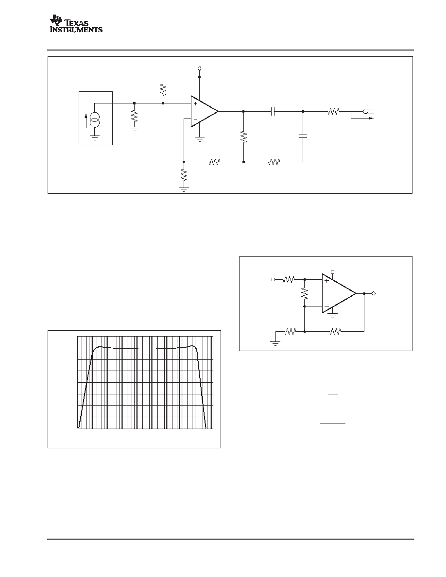
OPA830
SBOS263B - AUGUST 2004 - REVISED JANUARY 2005
www.ti.com
21
OPA830
325
528
78.7
650
+5V
845
1.87k
V
O
22
µ
F
47
µ
F
75
Video DAC
75
Load
Figure 5. Video Line Driver with SAG Correction
The input is shifted slightly positive in Figure 5 using the
voltage divider from the positive supply. This gives about
a 200mV input DC offset that will show up at the output pin
as a 400mV DC offset when the DAC output is at zero
current during the sync tip portion of the video signal. This
acts to hold the output in its linear operating region. This
will pass on any power-supply noise to the output with a
gain of approximately -20dB, so good supply decoupling
is recommended on the power-supply pin. Figure 6 shows
the frequency response for the circuit of Figure 5. This plot
shows the 8Hz low-frequency high-pass pole and a
high-end cutoff at approximately 100MHz.
3
0
-
3
-
6
-
9
-
12
-
15
-
18
-
21
Frequency (Hz)
N
o
r
m
a
liz
e
d
G
a
in
(
d
B
)
1
10
10
2
10
3
10
4
10
5
10
6
10
7
10
8
10
9
Figure 6. Video Line Driver Response to Matched
Load
NONINVERTING AMPLIFIER WITH REDUCED
PEAKING
Figure 7 shows a noninverting amplifier that reduces
peaking at low gains. The resistor R
C
compensates the
OPA830 to have higher Noise Gain (NG), which reduces
the AC response peaking (typically 5dB at G = +1 without
R
C
) without changing the DC gain. V
IN
needs to be a low
impedance source, such as an op amp. The resistor
values are low to reduce noise. Using both R
T
and R
F
helps minimize the impact of parasitic impedances.
OPA830
V
OUT
+5V
V
IN
R
G
R
T
R
F
R
C
Figure 7. Compensated Noninverting Amplifier
The Noise Gain can be calculated as follows:
G
1
+
1
)
R
F
R
G
G
2
+
1
)
R
T
)
R
F
G
1
R
C
NG
+
G
1
G
2
A unity-gain buffer can be designed by selecting
R
T
= R
F
= 20.0
and R
C
= 40.2
(do not use R
G
). This
gives a noise gain of 2, so the response will be similar to
the Characteristics Plots with G = +2. Decreasing R
C
to
20.0
will increase the noise gain to 3, which typically
gives a flat frequency response, but with less bandwidth.
The circuit in Figure 1 can be redesigned to have less
peaking by increasing the noise gain to 3. This is
accomplished by adding R
C
= 2.55k
across the op amp
inputs.
(1)
(2)
(3)

OPA830
SBOS263B - AUGUST 2004 - REVISED JANUARY 2005
www.ti.com
22
SINGLE-SUPPLY ACTIVE FILTER
The OPA830, while operating on a single +3V or +5V
supply, lends itself well to high-frequency active filter
designs. Again, the key additional requirement is to
establish the DC operating point of the signal near the
supply midpoint for highest dynamic range. Figure 8
shows an example design of a 1MHz low-pass Butterworth
filter using the Sallen-Key topology.
Both the input signal and the gain setting resistor are
AC-coupled using 0.1
µ
F blocking capacitors (actually
giving bandpass response with the low-frequency pole set
to 32kHz for the component values shown). As discussed
for Figure 1, this allows the midpoint bias formed by the
two 1.87k
resistors to appear at both the input and output
pins. The midband signal gain is set to +4 (12dB) in this
case. The capacitor to ground on the noninverting input is
intentionally set larger to dominate input parasitic terms. At
a gain of +4, the OPA830 on a single supply will show
30MHz small- and large-signal bandwidth. The resistor
values have been slightly adjusted to account for this
limited bandwidth in the amplifier stage. Tests of this circuit
show a precise 1MHz, -3dB point with a maximally-flat
passband (above the 32kHz AC-coupling corner), and a
maximum stop band attenuation of 36dB at the amplifier's
-3dB bandwidth of 30MHz.
DESIGN-IN TOOLS
DEMONSTRATION BOARDS
Several PC boards are available to assist in the initial
evaluation of circuit performance using the OPA830 in its
two package styles. Both of these are available, free, as
unpopulated PC boards delivered with descriptive
documentation. The summary information for these
boards is shown in Table 1.
Table 1. Demo Board Availability
PRODUCT
PACKAGE
DEMO BOARD
ORDERING
PRODUCT
PACKAGE
DEMO BOARD
NUMBER
ORDERING
NUMBER
OPA830ID
SO-8
DEM
-
OPA68xU
SBOU009
OPA830IDBV
SOT23-5
DEM
-
OPA6xxN
SBOU010
Go to the TI web site (www.ti.com) to request evaluation
boards through the OPA830 product folder.
OPA830
1.5k
1.87k
500
+5V
1.87k
4V
I
V
I
150pF
0.1
µ
F
1MHz, 2nd-Order
Butterworth Filter
100pF
432
137
0.1
µ
F
Figure 8. Single-Supply, High-Frequency Active Filter

OPA830
SBOS263B - AUGUST 2004 - REVISED JANUARY 2005
www.ti.com
23
MACROMODEL AND APPLICATIONS
SUPPORT
Computer simulation of circuit performance using SPICE
is often a quick way to analyze the performance of the
OPA830 and its circuit designs. This is particularly true for
video and RF amplifier circuits where parasitic
capacitance and inductance can play a major role on
circuit performance. A SPICE model for the OPA830 is
available through the TI web page (www.ti.com). The
applications department is also available for design
assistance. These models predict typical small signal AC,
transient steps, DC performance, and noise under a wide
variety of operating conditions. The models include the
noise terms found in the electrical specifications of the
data sheet. These models do not attempt to distinguish
between the package types in their small-signal AC
performance.
OPERATING SUGGESTIONS
OPTIMIZING RESISTOR VALUES
Since the OPA830 is a unity-gain stable, voltage-feedback
op amp, a wide range of resistor values may be used for
the feedback and gain setting resistors. The primary limits
on these values are set by dynamic range (noise and
distortion) and parasitic capacitance considerations. For a
noninverting unity-gain follower application, the feedback
connection should be made with a direct short.
Below 200
, the feedback network will present additional
output loading which can degrade the harmonic distortion
performance of the OPA830. Above 1k
, the typical
parasitic capacitance (approximately 0.2pF) across the
feedback resistor may cause unintentional band limiting in
the amplifier response.
A good rule of thumb is to target the parallel combination
of R
F
and R
G
(see Figure 3) to be less than about 400
.
The combined impedance R
F
|| R
G
interacts with the
inverting input capacitance, placing an additional pole in
the feedback network, and thus a zero in the forward
response. Assuming a 2pF total parasitic on the inverting
node, holding R
F
|| R
G
< 400
will keep this pole above
200MHz. By itself, this constraint implies that the feedback
resistor R
F
can increase to several k
at high gains. This
is acceptable as long as the pole formed by R
F
and any
parasitic capacitance appearing in parallel is kept out of
the frequency range of interest.
In the inverting configuration, an additional design
consideration must be noted. R
G
becomes the input
resistor and therefore the load impedance to the driving
source. If impedance matching is desired, R
G
may be set
equal to the required termination value. However, at low
inverting gains, the resultant feedback resistor value can
present a significant load to the amplifier output. For
example, an inverting gain of 2 with a 50
input matching
resistor (= R
G
) would require a 100
feedback resistor,
which would contribute to output loading in parallel with the
external load. In such a case, it would be preferable to
increase both the R
F
and R
G
values, and then achieve the
input matching impedance with a third resistor to ground
(see Figure 9). The total input impedance becomes the
parallel combination of R
G
and the additional shunt
resistor.
BANDWIDTH vs GAIN:
NONINVERTING OPERATION
Voltage-feedback op amps exhibit decreasing closed-loop
bandwidth as the signal gain is increased. In theory, this
relationship is described by the Gain Bandwidth Product
(GBP) shown in the specifications. Ideally, dividing GBP
by the noninverting signal gain (also called the Noise Gain,
or NG) will predict the closed-loop bandwidth. In practice,
this only holds true when the phase margin approaches
90
∞
, as it does in high-gain configurations. At low gains
(increased feedback factors), most amplifiers will exhibit a
more complex response with lower phase margin. The
OPA830 is compensated to give a slightly peaked
response in a noninverting gain of 2 (see Figure 3). This
results in a typical gain of +2 bandwidth of 110MHz, far
exceeding that predicted by dividing the 110MHz GBP by
2. Increasing the gain will cause the phase margin to
approach 90
∞
and the bandwidth to more closely approach
the predicted value of (GBP/NG). At a gain of +10, the
11MHz bandwidth shown in the Electrical Characteristics
agrees with that predicted using the simple formula and
the typical GBP of 110MHz.
Frequency response in a gain of +2 may be modified to
achieve exceptional flatness simply by increasing the
noise gain to 3. One way to do this, without affecting the +2
signal gain, is to add an 2.55k
resistor across the two
inputs, as shown in Figure 7. A similar technique may be
used to reduce peaking in unity-gain (voltage follower)
applications. For example, by using a 750
feedback
resistor along with a 750
resistor across the two op amp
inputs, the voltage follower response will be similar to the
gain of +2 response of Figure 2. Further reducing the value
of the resistor across the op amp inputs will further dampen
the frequency response due to increased noise gain. The
OPA830 exhibits minimal bandwidth reduction going to
single-supply (+5V) operation as compared with
±
5V. This
minimal reduction is because the internal bias control
circuitry retains nearly constant quiescent current as the
total supply voltage between the supply pins is changed.
INVERTING AMPLIFIER OPERATION
All of the familiar op amp application circuits are available
with the OPA830 to the designer. See Figure 9 for a typical
inverting configuration where the I/O impedances and
signal gain from Figure 1 are retained in an inverting circuit
configuration. Inverting operation is one of the more
common requirements and offers several performance
benefits. It also allows the input to be biased at V
S
/2
without any headroom issues. The output voltage can be
independently moved to be within the output voltage range
with coupling capacitors, or bias adjustment resistors.

OPA830
SBOS263B - AUGUST 2004 - REVISED JANUARY 2005
www.ti.com
24
OPA830
50
Source
R
F
750
R
G
374
2R
T
1.5k
R
M
57.6
+5V
2R
T
1.5k
150
0.1
µ
F
6.8
µ
F
+
0.1
µ
F
0.1
µ
F
+V
S
2
Figure 9. AC-Coupled, G = -2 Example Circuit
In the inverting configuration, three key design
considerations must be noted. The first consideration is
that the gain resistor (R
G
) becomes part of the signal
channel input impedance. If input impedance matching is
desired (which is beneficial whenever the signal is coupled
through a cable, twisted pair, long PC board trace, or other
transmission line conductor), R
G
may be set equal to the
required termination value and R
F
adjusted to give the
desired gain. This is the simplest approach and results in
optimum bandwidth and noise performance.
However, at low inverting gains, the resulting feedback
resistor value can present a significant load to the amplifier
output. For an inverting gain of 2, setting R
G
to 50
for
input matching eliminates the need for R
M
but requires a
100
feedback resistor. This configuration has the
interesting advantage of the noise gain becoming equal to
2 for a 50
source impedance--the same as the
noninverting circuits considered above. The amplifier
output will now see the 100
feedback resistor in parallel
with the external load. In general, the feedback resistor
should be limited to the 200
to 1.5k
range. In this case,
it is preferable to increase both the R
F
and R
G
values, as
shown in Figure 9, and then achieve the input matching
impedance with a third resistor (R
M
) to ground. The total
input impedance becomes the parallel combination of R
G
and R
M
.
The second major consideration, touched on in the
previous paragraph, is that the signal source impedance
becomes part of the noise gain equation and hence
influences the bandwidth. For the example in Figure 9, the
R
M
value combines in parallel with the external 50
source impedance (at high frequencies), yielding an
effective driving impedance of 50
|| 57.6
= 26.8
. This
impedance is added in series with R
G
for calculating the
noise gain. The resulting noise gain is 2.87 for Figure 9, as
opposed to only 2 if R
M
could be eliminated as discussed
above. The bandwidth will therefore be lower for the gain
of -2 circuit of Figure 9 (NG = +2.87) than for the gain of
+2 circuit of Figure 1.
The third important consideration in inverting amplifier
design is setting the bias current cancellation resistors on
the noninverting input (a parallel combination of
R
T
= 750
). If this resistor is set equal to the total DC
resistance looking out of the inverting node, the output DC
error, due to the input bias currents, will be reduced to
(Input Offset Current) times R
F
. With the DC blocking
capacitor in series with R
G
, the DC source impedance
looking out of the inverting mode is simply R
F
= 750
for
Figure 9. To reduce the additional high-frequency noise
introduced by this resistor and power-supply feed-through,
R
T
is bypassed with a capacitor.
OUTPUT CURRENT AND VOLTAGES
The OPA830 provides outstanding output voltage
capability. For the +5V supply, under no-load conditions at
+25
∞
C, the output voltage typically swings closer than
90mV to either supply rail.
The minimum specified output voltage and current
specifications over temperature are set by worst-case
simulations at the cold temperature extreme. Only at cold
startup will the output current and voltage decrease to the
numbers shown in the ensured tables. As the output
transistors deliver power, their junction temperatures will
increase, decreasing their V
BE
s (increasing the available
output voltage swing) and increasing their current gains
(increasing the available output current). In steady-state
operation, the available output voltage and current will
always be greater than that shown in the over-temperature
specifications, since the output stage junction
temperatures will be higher than the minimum specified
operating ambient.
To maintain maximum output stage linearity, no output
short-circuit protection is provided. This will not normally
be a problem, since most applications include a series
matching resistor at the output that will limit the internal
power dissipation if the output side of this resistor is
shorted to ground. However, shorting the output pin
directly to the adjacent positive power-supply pin (8-pin
packages) will, in most cases, destroy the amplifier. If
additional short-circuit protection is required, consider a
small series resistor in the power-supply leads. This will
reduce the available output voltage swing under heavy
output loads.
DRIVING CAPACITIVE LOADS
One of the most demanding and yet very common load
conditions for an op amp is capacitive loading. Often, the
capacitive load is the input of an ADC--including
additional external capacitance which may be recom-
mended to improve ADC linearity. A high-speed, high
open-loop gain amplifier like the OPA830 can be very
susceptible to decreased stability and closed-loop
response peaking when a capacitive load is placed directly
on the output pin. When the primary considerations are
frequency response flatness, pulse response fidelity,
and/or distortion, the simplest and most effective solution

OPA830
SBOS263B - AUGUST 2004 - REVISED JANUARY 2005
www.ti.com
25
is to isolate the capacitive load from the feedback loop by
inserting a series isolation resistor between the amplifier
output and the capacitive load.
The Typical Characteristic curves show the recommended
R
S
versus capacitive load and the resulting frequency
response at the load. Parasitic capacitive loads greater
than 2pF can begin to degrade the performance of the
OPA830. Long PC board traces, unmatched cables, and
connections to multiple devices can easily exceed this
value. Always consider this effect carefully, and add the
recommended series resistor as close as possible to the
output pin (see the Board Layout Guidelines section).
The criterion for setting this R
S
resistor is a maximum
bandwidth, flat frequency response at the load. For a gain
of +2, the frequency response at the output pin is already
slightly peaked without the capacitive load, requiring
relatively high values of R
S
to flatten the response at the
load. Increasing the noise gain will also reduce the peaking
(see Figure 7).
DISTORTION PERFORMANCE
The OPA830 provides good distortion performance into a
150
load. Relative to alternative solutions, it provides
exceptional performance into lighter loads and/or
operating on a single +3V supply. Generally, until the
fundamental signal reaches very high frequency or power
levels, the 2nd-harmonic will dominate the distortion with
a negligible 3rd-harmonic component. Focusing then on
the 2nd-harmonic, increasing the load impedance
improves distortion directly. Remember that the total load
includes the feedback network; in the noninverting
configuration (see Figure 3) this is sum of R
F
+ R
G
, while
in the inverting configuration, only R
F
needs to be included
in parallel with the actual load. Running differential
suppresses the 2nd-harmonic, as shown in the differential
typical characteristic curves.
NOISE PERFORMANCE
High slew rate, unity-gain stable, voltage-feedback op
amps usually achieve their slew rate at the expense of a
higher input noise voltage. The 9.2nV/
Hz input voltage
noise for the OPA830 however, is much lower than
comparable amplifiers. The input-referred voltage noise
and the two input-referred current noise terms (2.8pA/
Hz)
combine to give low output noise under a wide variety of
operating conditions. Figure 10 shows the op amp noise
analysis model with all the noise terms included. In this
model, all noise terms are taken to be noise voltage or
current density terms in either nV/
Hz or pA/
Hz.
4kT
R
G
R
G
R
F
R
S
OPA830
I
BI
E
O
I
BN
4kT = 1.6E
-
20J
at 290
_
K
E
RS
E
NI
4kTR
S
4kTR
F
Figure 10. Noise Analysis Model
The total output spot noise voltage can be computed as the
square root of the sum of all squared output noise voltage
contributors. Equation 4 shows the general form for the
output noise voltage using the terms shown in Figure 10:
E
O
+
ENI
2
)
IBNRS
2
)
4kTR
S
NG2
)
IBIRF
2
)
4kTRFNG
Dividing this expression by the noise gain
(NG = (1 + R
F
/R
G
)) will give the equivalent input-referred
spot noise voltage at the noninverting input, as shown in
Equation 5:
E
N
+
E
NI
2
)
I
BN
R
S
2
)
4kTR
S
)
I
BI
R
F
NG
2
)
4kTR
F
NG
Evaluating these two equations for the circuit and
component values shown in Figure 1 will give a total output
spot noise voltage of 19.3nV/
Hz and a total equivalent
input spot noise voltage of 9.65nV/
Hz. This is including
the noise added by the resistors. This total input-referred
spot noise voltage is not much higher than the 9.2nV/
Hz
specification for the op amp voltage noise alone.
DC ACCURACY AND OFFSET CONTROL
The balanced input stage of a wideband voltage-feedback
op amp allows good output DC accuracy in a wide variety
of applications. The power-supply current trim for the
OPA830 gives even tighter control than comparable
products. Although the high-speed input stage does
require relatively high input bias current (typically 5
µ
A out
of each input terminal), the close matching between them
may be used to reduce the output DC error caused by this
current. This is done by matching the DC source
resistances appearing at the two inputs. Evaluating the
configuration of Figure 3 (which has matched DC input
(4)
(5)

OPA830
SBOS263B - AUGUST 2004 - REVISED JANUARY 2005
www.ti.com
26
resistances), using worst-case +25
∞
C input offset voltage
and current specifications, gives a worst-case output
offset voltage equal to:
(NG = noninverting signal gain at DC)
±
(NG
◊
V
OS(MAX)
) + (R
F
◊
I
OS(MAX)
)
=
±
(2
◊
7mV)
◊
(375
◊
1
µ
A)
=
±
14.38mV
A fine-scale output offset null, or DC operating point
adjustment, is often required. Numerous techniques are
available for introducing DC offset control into an op amp
circuit. Most of these techniques are based on adding a DC
current through the feedback resistor. In selecting an offset
trim method, one key consideration is the impact on the
desired signal path frequency response. If the signal path
is intended to be noninverting, the offset control is best
applied as an inverting summing signal to avoid interaction
with the signal source. If the signal path is intended to be
inverting, applying the offset control to the noninverting
input may be considered. Bring the DC offsetting current
into the inverting input node through resistor values that
are much larger than the signal path resistors. This will
insure that the adjustment circuit has minimal effect on the
loop gain and hence the frequency response.
THERMAL ANALYSIS
Maximum desired junction temperature will set the
maximum allowed internal power dissipation, as
described below. In no case should the maximum junction
temperature be allowed to exceed 150
∞
C.
Operating junction temperature (T
J
) is given by
T
A
+ P
D
◊ q
JA
. The total internal power dissipation (P
D
)
is the sum of quiescent power (P
DQ
) and additional
power dissipated in the output stage (P
DL
) to deliver load
power. Quiescent power is simply the specified no-load
supply current times the total supply voltage across the
part. P
DL
will depend on the required output signal and
load; though, for resistive loads connected to
mid-supply (V
S
/2), P
DL
is at a maximum when the output
is fixed at a voltage equal to V
S
/4 or 3V
S
/4. Under this
condition, P
DL
= V
S
2
/(16
◊
R
L
), where R
L
includes
feedback network loading.
Note that it is the power in the output stage, and not into the
load, that determines internal power dissipation.
As a worst-case example, compute the maximum T
J
using
an OPA830 (SOT23-5 package) in the circuit of Figure 1
operating at the maximum specified ambient temperature
of +85
∞
C and driving a 150
load at mid-supply.
P
D
= 10V
◊
3.9mA + 5
2
/(16
◊
(150
|| 750
)) = 51.5mW
Maximum T
J
= +85
∞
C + (0.051W
◊
150
∞
C/W) = 93
∞
C.
Although this is still well below the specified maximum
junction temperature, system reliability considerations
may require lower ensured junction temperatures. The
highest possible internal dissipation will occur if the load
requires current to be forced into the output at high output
voltages or sourced from the output at low output voltages.
This puts a high current through a large internal voltage
drop in the output transistors.
BOARD LAYOUT GUIDELINES
Achieving optimum performance with a high-frequency
amplifier like the OPA830 requires careful attention to
board layout parasitics and external component types.
Recommendations that will optimize performance include:
a) Minimize parasitic capacitance to any AC ground for
all of the signal I/O pins. Parasitic capacitance on the
output and inverting input pins can cause instability: on the
noninverting input, it can react with the source impedance
to cause unintentional bandlimiting. To reduce unwanted
capacitance, a window around the signal I/O pins should
be opened in all of the ground and power planes around
those pins. Otherwise, ground and power planes should
be unbroken elsewhere on the board.
b) Minimize the distance ( < 0.25") from the power-supply
pins to high-frequency 0.1
µ
F decoupling capacitors. At the
device pins, the ground and power-plane layout should not
be in close proximity to the signal I/O pins. Avoid narrow
power and ground traces to minimize inductance between
the pins and the decoupling capacitors. Each power-
supply connection should always be decoupled with one
of these capacitors. An optional supply decoupling
capacitor (0.1
µ
F) across the two power supplies (for
bipolar operation) will improve 2nd-harmonic distortion
performance. Larger (2.2
µ
F to 6.8
µ
F) decoupling
capacitors, effective at lower frequency, should also be
used on the main supply pins. These may be placed
somewhat farther from the device and may be shared
among several devices in the same area of the PC board.
c) Careful selection and placement of external
components will preserve the high-frequency perfor-
mance. Resistors should be a very low reactance type.
Surface-mount resistors work best and allow a tighter
overall layout. Metal film or carbon composition
axially-leaded resistors can also provide good high-
frequency performance. Again, keep their leads and PC
board traces as short as possible. Never use wire-wound
type resistors in a high-frequency application. Since the
output pin and inverting input pin are the most sensitive to
parasitic capacitance, always position the feedback and
series output resistor, if any, as close as possible to the
output pin. Other network components, such as
noninverting input termination resistors, should also be
placed close to the package. Where double-side
component mounting is allowed, place the feedback
resistor directly under the package on the other side of the
board between the output and inverting input pins. Even
with a low parasitic capacitance shunting the external
resistors, excessively high resistor values can create
OPA830
SBOS263B - AUGUST 2004 - REVISED JANUARY 2005
www.ti.com
27
significant time constants that can degrade performance.
Good axial metal film or surface-mount resistors have
approximately 0.2pF in shunt with the resistor. For resistor
values > 1.5k
, this parasitic capacitance can add a pole
and/or zero below 500MHz that can effect circuit
operation. Keep resistor values as low as possible
consistent with load driving considerations. The 750
feedback used in the Typical Characteristics is a good
starting point for design.
d) Connections to other wideband devices on the board
may be made with short direct traces or through onboard
transmission lines. For short connections, consider the
trace and the input to the next device as a lumped
capacitive load. Relatively wide traces (50mils to 100mils)
should be used, preferably with ground and power planes
opened up around them. Estimate the total capacitive load
and set R
S
from the typical characteristic curve
Recommended R
S
vs Capacitive Load. Low parasitic
capacitive loads (< 5pF) may not need an R
S
since the
OPA830 is nominally compensated to operate with a 2pF
parasitic load. Higher parasitic capacitive loads without an
R
S
are allowed as the signal gain increases (increasing the
unloaded phase margin). If a long trace is required, and the
6dB signal loss intrinsic to a doubly-terminated
transmission line is acceptable, implement a matched
impedance transmission line using microstrip or stripline
techniques (consult an ECL design handbook for
microstrip and stripline layout techniques). A 50
environment is normally not necessary onboard, and in
fact, a higher impedance environment will improve
distortion as shown in the distortion versus load plots. With
a characteristic board trace impedance defined (based on
board material and trace dimensions), a matching series
resistor into the trace from the output of the OPA830 is
used as well as a terminating shunt resistor at the input of
the destination device. Remember also that the
terminating impedance will be the parallel combination of
the shunt resistor and the input impedance of the
destination device; this total effective impedance should
be set to match the trace impedance. If the 6dB attenuation
of a doubly-terminated transmission line is unacceptable,
a long trace can be series-terminated at the source end
only. Treat the trace as a capacitive load in this case and
set the series resistor value as shown in the typical
characteristic curve Recommended R
S
vs Capacitive
Load. This will not preserve signal integrity as well as a
doubly-terminated line. If the input impedance of the
destination device is low, there will be some signal
attenuation due to the voltage divider formed by the series
output into the terminating impedance.
e) Socketing a high-speed part is not recommended.
The additional lead length and pin-to-pin capacitance
introduced by the socket can create an extremely
troublesome parasitic network which can make it almost
impossible to achieve a smooth, stable frequency
response. Best results are obtained by soldering the
OPA830 onto the board.
INPUT AND ESD PROTECTION
The OPA830 is built using a very high-speed complemen-
tary bipolar process. The internal junction breakdown
voltages are relatively low for these very small geometry
devices. These breakdowns are reflected in the Absolute
Maximum Ratings table. All device pins are protected with
internal ESD protection diodes to the power supplies, as
shown in Figure 11.
External
Pin
+V
CC
- V
CC
Internal
Circuitry
Figure 11. Internal ESD Protection
These diodes provide moderate protection to input
overdrive voltages above the supplies as well. The
protection diodes can typically support 30mA continuous
current. Where higher currents are possible (that is, in
systems with
±
15V supply parts driving into the OPA830),
current-limiting series resistors should be added into the
two inputs. Keep these resistor values as low as possible,
since high values degrade both noise performance and
frequency response.

PACKAGING INFORMATION
Orderable Device
Status
(1)
Package
Type
Package
Drawing
Pins Package
Qty
Eco Plan
(2)
Lead/Ball Finish
MSL Peak Temp
(3)
OPA830ID
ACTIVE
SOIC
D
8
100
None
CU SNPB
Level-3-260C-168 HR
OPA830IDBVR
ACTIVE
SOT-23
DBV
5
3000 Green (RoHS &
no Sb/Br)
CU NIPDAU
Level-1-260C-UNLIM
OPA830IDBVT
ACTIVE
SOT-23
DBV
5
250
Green (RoHS &
no Sb/Br)
CU NIPDAU
Level-1-260C-UNLIM
OPA830IDR
ACTIVE
SOIC
D
8
2500
None
CU SNPB
Level-3-260C-168 HR
(1)
The marketing status values are defined as follows:
ACTIVE: Product device recommended for new designs.
LIFEBUY: TI has announced that the device will be discontinued, and a lifetime-buy period is in effect.
NRND: Not recommended for new designs. Device is in production to support existing customers, but TI does not recommend using this part in
a new design.
PREVIEW: Device has been announced but is not in production. Samples may or may not be available.
OBSOLETE: TI has discontinued the production of the device.
(2)
Eco Plan - May not be currently available - please check
http://www.ti.com/productcontent
for the latest availability information and additional
product content details.
None: Not yet available Lead (Pb-Free).
Pb-Free (RoHS): TI's terms "Lead-Free" or "Pb-Free" mean semiconductor products that are compatible with the current RoHS requirements
for all 6 substances, including the requirement that lead not exceed 0.1% by weight in homogeneous materials. Where designed to be soldered
at high temperatures, TI Pb-Free products are suitable for use in specified lead-free processes.
Green (RoHS & no Sb/Br): TI defines "Green" to mean "Pb-Free" and in addition, uses package materials that do not contain halogens,
including bromine (Br) or antimony (Sb) above 0.1% of total product weight.
(3)
MSL, Peak Temp. -- The Moisture Sensitivity Level rating according to the JEDECindustry standard classifications, and peak solder
temperature.
Important Information and Disclaimer:The information provided on this page represents TI's knowledge and belief as of the date that it is
provided. TI bases its knowledge and belief on information provided by third parties, and makes no representation or warranty as to the
accuracy of such information. Efforts are underway to better integrate information from third parties. TI has taken and continues to take
reasonable steps to provide representative and accurate information but may not have conducted destructive testing or chemical analysis on
incoming materials and chemicals. TI and TI suppliers consider certain information to be proprietary, and thus CAS numbers and other limited
information may not be available for release.
In no event shall TI's liability arising out of such information exceed the total purchase price of the TI part(s) at issue in this document sold by TI
to Customer on an annual basis.
PACKAGE OPTION ADDENDUM
www.ti.com
18-Jan-2005
Addendum-Page 1


IMPORTANT NOTICE
Texas Instruments Incorporated and its subsidiaries (TI) reserve the right to make corrections, modifications,
enhancements, improvements, and other changes to its products and services at any time and to discontinue
any product or service without notice. Customers should obtain the latest relevant information before placing
orders and should verify that such information is current and complete. All products are sold subject to TI's terms
and conditions of sale supplied at the time of order acknowledgment.
TI warrants performance of its hardware products to the specifications applicable at the time of sale in
accordance with TI's standard warranty. Testing and other quality control techniques are used to the extent TI
deems necessary to support this warranty. Except where mandated by government requirements, testing of all
parameters of each product is not necessarily performed.
TI assumes no liability for applications assistance or customer product design. Customers are responsible for
their products and applications using TI components. To minimize the risks associated with customer products
and applications, customers should provide adequate design and operating safeguards.
TI does not warrant or represent that any license, either express or implied, is granted under any TI patent right,
copyright, mask work right, or other TI intellectual property right relating to any combination, machine, or process
in which TI products or services are used. Information published by TI regarding third-party products or services
does not constitute a license from TI to use such products or services or a warranty or endorsement thereof.
Use of such information may require a license from a third party under the patents or other intellectual property
of the third party, or a license from TI under the patents or other intellectual property of TI.
Reproduction of information in TI data books or data sheets is permissible only if reproduction is without
alteration and is accompanied by all associated warranties, conditions, limitations, and notices. Reproduction
of this information with alteration is an unfair and deceptive business practice. TI is not responsible or liable for
such altered documentation.
Resale of TI products or services with statements different from or beyond the parameters stated by TI for that
product or service voids all express and any implied warranties for the associated TI product or service and
is an unfair and deceptive business practice. TI is not responsible or liable for any such statements.
Following are URLs where you can obtain information on other Texas Instruments products and application
solutions:
Products
Applications
Amplifiers
amplifier.ti.com
Audio
www.ti.com/audio
Data Converters
dataconverter.ti.com
Automotive
www.ti.com/automotive
DSP
dsp.ti.com
Broadband
www.ti.com/broadband
Interface
interface.ti.com
Digital Control
www.ti.com/digitalcontrol
Logic
logic.ti.com
Military
www.ti.com/military
Power Mgmt
power.ti.com
Optical Networking
www.ti.com/opticalnetwork
Microcontrollers
microcontroller.ti.com
Security
www.ti.com/security
Telephony
www.ti.com/telephony
Video & Imaging
www.ti.com/video
Wireless
www.ti.com/wireless
Mailing Address:
Texas Instruments
Post Office Box 655303 Dallas, Texas 75265
Copyright
2005, Texas Instruments Incorporated