 | ÐлекÑÑоннÑй компоненÑ: OPA692IDR | СкаÑаÑÑ:  PDF PDF  ZIP ZIP |
Äîêóìåíòàöèÿ è îïèñàíèÿ www.docs.chipfind.ru
OPA692
SBOS236C MARCH 2002 REVISED JANUARY 2003
www.ti.com
DESCRIPTION
The OPA692 provides an easy to use, broadband fixed gain
video buffer amplifier. Depending on the external connec-
tions, the internal resistor network may be used to provide
either a fixed gain of +2 video buffer or a gain of +1 or 1
voltage buffer. Operating on a very low 5.1mA supply cur-
rent, the OPA692 offers a slew rate and output power
normally associated with a much higher supply current. A
new output stage architecture delivers high output current
with minimal headroom and crossover distortion. This gives
exceptional single-supply operation. Using a single +5V
supply, the OPA692 can deliver a 1V to 4V output swing with
over 120mA drive current and > 200MHz bandwidth. This
combination of features makes the OPA692 an ideal RGB
line driver or single-supply Analog-to-Digital Converter (ADC)
input driver.
The low 5.1mA supply current for the OPA692 is precisely
trimmed at +25
°
C. This trim, along with low drift over tem-
perature, ensures a lower maximum supply current than
competing products that report only a room temperature
nominal supply current. System power may be further re-
duced by using the optional disable control pin. Leaving this
disable pin open, or holding it HIGH, gives normal operation.
If pulled LOW, the OPA692 supply current drops to less than
150
µ
A while the I/O pins go into a high-impedance state.
FEATURES
q
FLEXIBLE SUPPLY RANGE:
+5V to +12V Single Supply
±
2.5V to
±
6V Dual Supplies
q
INTERNALLY FIXED GAIN: +2 or
±
1
q
HIGH BANDWIDTH (G = +2): 225MHz
q
LOW SUPPLY CURRENT: 5.1mA
q
LOW DISABLED CURRENT: 150
µ
A
q
HIGH OUTPUT CURRENT: 190mA
q
OUTPUT VOLTAGE SWING:
±
4.0V
q
SOT23-6 AVAILABLE
Copyright © 2002-2003, Texas Instruments Incorporated
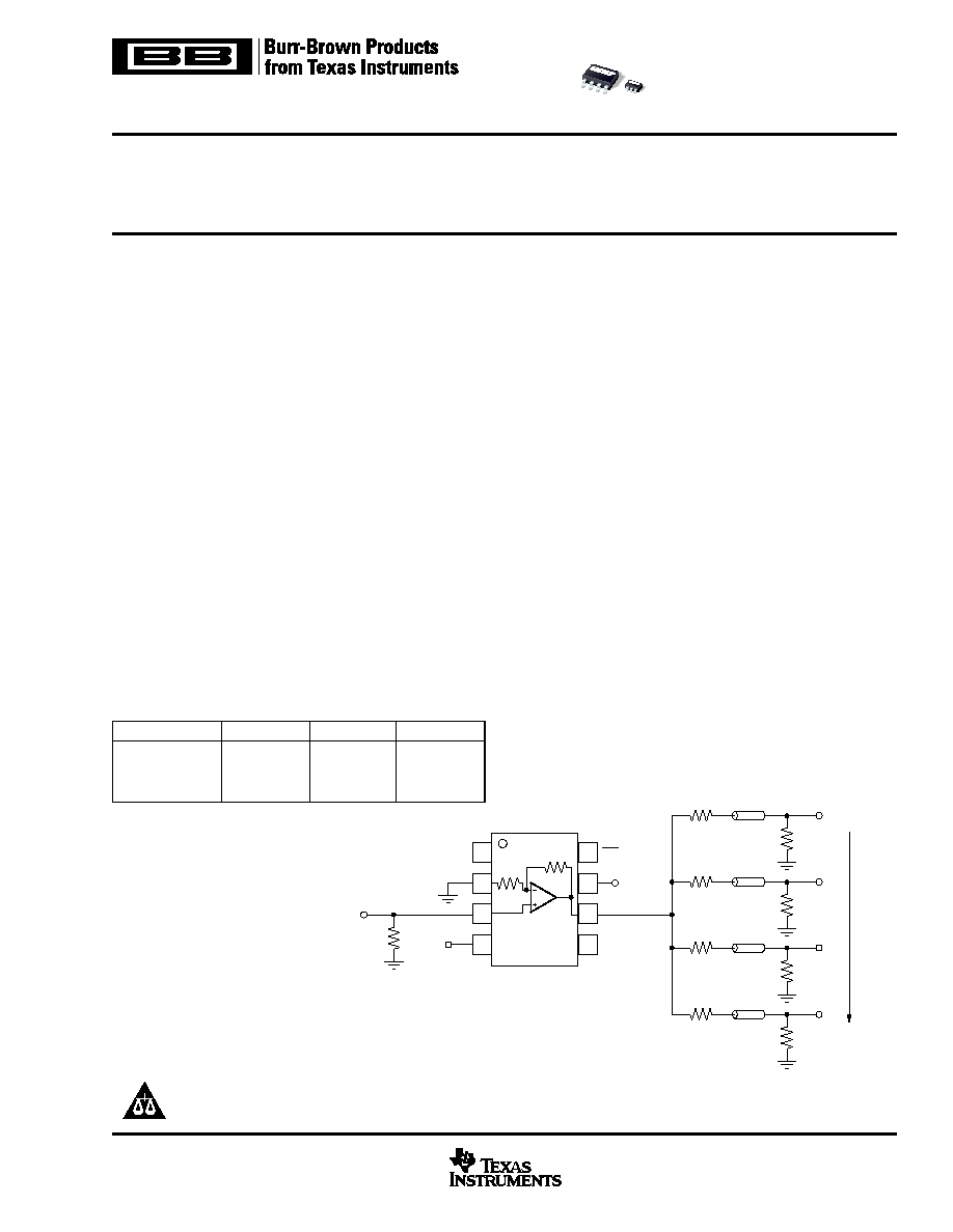
Wideband, Fixed Gain
Video BUFFER AMPLIFIER With Disable
Please be aware that an important notice concerning availability, standard warranty, and use in critical applications of
Texas Instruments semiconductor products and disclaimers thereto appears at the end of this data sheet.
APPLICATIONS
q
BROADBAND VIDEO LINE DRIVERS
q
MULTIPLE LINE VIDEO DA
q
PORTABLE INSTRUMENTS
q
ADC BUFFERS
q
ACTIVE FILTERS
OPA6
92
OPA6
92
OPA692 RELATED PRODUCTS
SINGLES
DUALS
TRIPLES
Voltage-Feedback
OPA690
OPA2690
OPA3690
Current-Feedback
OPA691
OPA2691
OPA3691
Fixed Gain
OPA682
OPA2682
OPA3692
Video
Out
75
75
RG-59
75
75
RG-59
75
75
RG-59
75
75
RG-59
75
1
2
3
4
8
7
6
5
DIS
OPA692
SO-8
G = +2
+5V
5V
Video
In
PRODUCTION DATA information is current as of publication date.
Products conform to specifications per the terms of Texas Instruments
standard warranty. Production processing does not necessarily include
testing of all parameters.
225MHz, 4-Output Component Video DA
OPA692
2
SBOS236C
www.ti.com
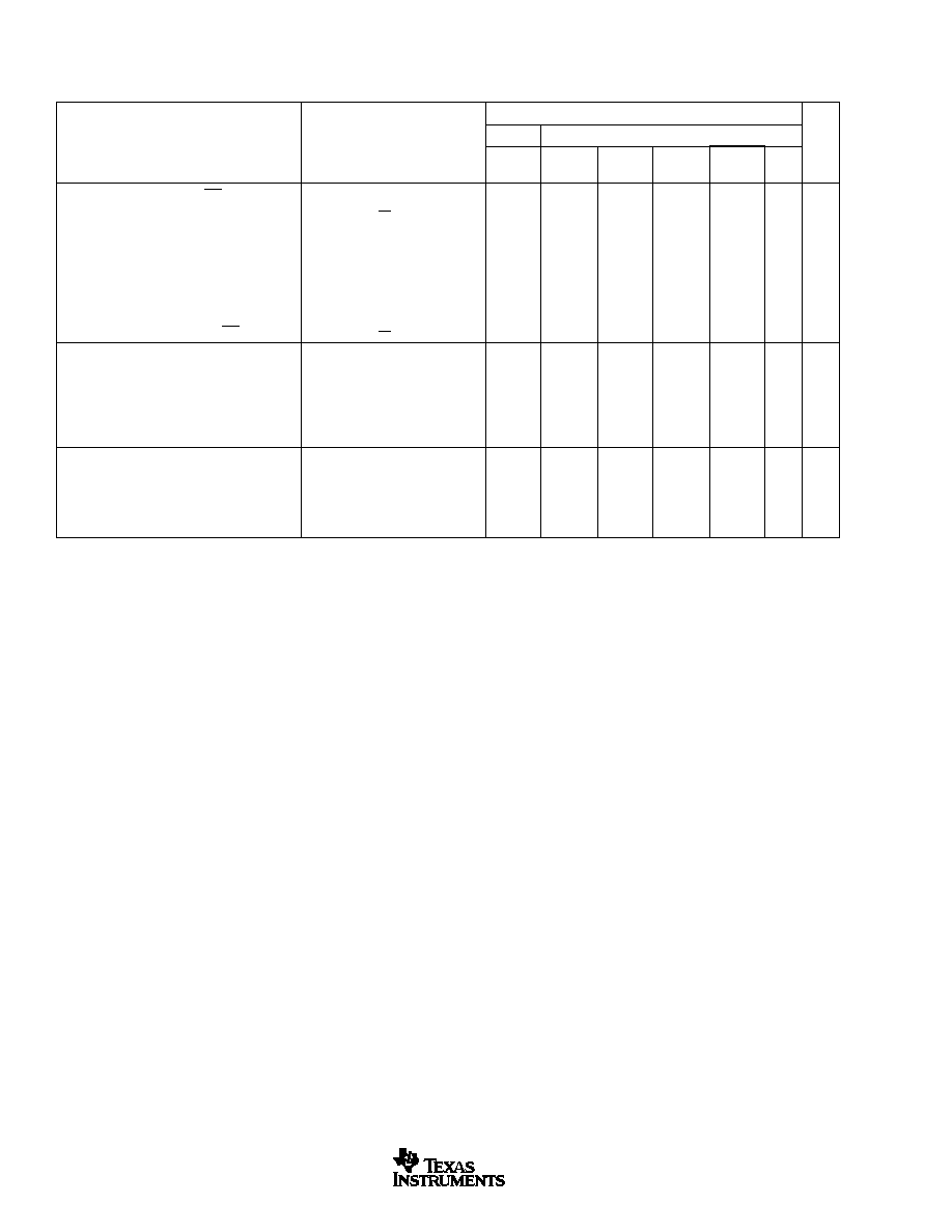
SPECIFIED
PACKAGE
TEMPERATURE
PACKAGE
ORDERING
TRANSPORT
PRODUCT
PACKAGE-LEAD
DESIGNATOR
(1)
RANGE
MARKING
NUMBER
MEDIA, QUANTITY
OPA692ID
SO-8 Surface-Mount
D
40
°
C to +85
°
C
OPA692
OPA692ID
Rails, 100
"
"
"
"
"
OPA692IDR
Tape and Reel, 2500
OPA692IDBV
SOT23-6
DBV
40
°
C to +85
°
C
OAGI
OPA692IDBVT
Tape and Reel, 250
"
"
"
"
"
OPA692IDBVR
Tape and Reel, 3000
NOTES: (1) For the most current specifications and package information, refer to our web site at www.ti.com.
ABSOLUTE MAXIMUM RATINGS
(1)
Power Supply ...............................................................................
±
6.5V
DC
Internal Power Dissipation
(2)
............................ See Thermal Information
Differential Input Voltage
(3)
...............................................................
±
1.2V
Input Voltage Range ............................................................................
±
V
S
Storage Temperature Range: D, DVB ........................... 40
°
C to +125
°
C
Lead Temperature (soldering, 10s) .............................................. +300
°
C
Junction Temperature (T
J
) ........................................................... +175
°
C
ESD Resistance: HBM ........................................................................ 2kV
MM ........................................................................ 200V
NOTES: (1) Stresses above these ratings may cause permanent damage.
Exposure to absolute maximum conditions for extended periods may degrade
device reliability. These are stress ratings only, and functional operation of the
device at these or any other conditions beyond those specified is not implied.
(2) Packages must be derated based on specified
JA
. Maximum T
J
must be
observed. (3) Noninverting input to internal inverting node.
ELECTROSTATIC
DISCHARGE SENSITIVITY
This integrated circuit can be damaged by ESD. Texas Instru-
ments recommends that all integrated circuits be handled with
appropriate precautions. Failure to observe proper handling
and installation procedures can cause damage.
ESD damage can range from subtle performance degrada-
tion to complete device failure. Precision integrated circuits
may be more susceptible to damage because very small
parametric changes could cause the device not to meet its
published specifications.
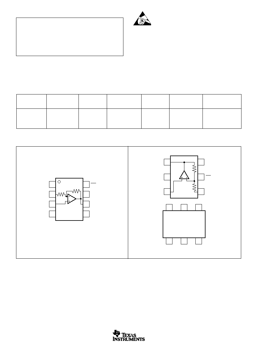
PIN CONFIGURATION
Top View
SO
Top View
SOT
PACKAGE/ORDERING INFORMATION
1
2
3
4
8
7
6
5
DIS
+V
S
Output
NC
R
F
402
R
G
402
NC
IN
+IN
V
S
NC: No Connection
1
2
3
6
5
4
Output
V
S
+IN
+V
S
DIS
IN
R
F
402
R
G
402
1
2
3
6
5
4
OAGI
Pin Orientation/Package Marking
OPA692
3
SBOS236C
www.ti.com
ELECTRICAL CHARACTERISTICS:
V
S
=
±
5V
Boldface limits are tested at +25
°
C.
G = +2 (IN grounded) and R
L
= 100
(see Figure 1 for AC performance only), unless otherwise noted.
OPA692ID, IDBV
TYP
MIN/MAX OVER TEMPERATURE
0
°
C to
40
°
C to
MIN/
TEST
PARAMETER
CONDITIONS
+25
°
C
+25
°
C
(1)
70
°
C
+85
°
C
UNITS
MAX
LEVEL
(2 )
AC PERFORMANCE (see Figure 1)
Small-Signal Bandwidth (V
O
< 0.5Vp-p)
G = +1
280
MHz
typ
C
G = +2
225
185
180
170
MHz
min
B
G = 1
220
MHz
typ
C
Bandwidth for 0.1dB Gain Flatness
G = +2, V
O
< 0.5Vp-p
120
40
35
30
MHz
min
B
Peaking at a Gain of +1
V
O
< 0.5Vp-p
0.2
1
1.5
2
dB
max
B
Large-Signal Bandwidth
G = +2, V
O
= 5Vp-p
220
MHz
typ
C
Slew Rate
G = +2, 4V Step
2000
1400
1375
1350
V/
µ
s
min
B
Rise-and-Fall Time
G = +2, V
O
= 0.5V Step
1.6
ns
typ
C
G = +2, V
O
= 5V Step
1.9
ns
typ
C
Settling Time to 0.02%
G = +2, V
O
= 2V Step
12
ns
typ
C
0.1%
G = +2, V
O
= 2V Step
8
ns
typ
C
Harmonic Distortion
G = +2, f = 5MHz, V
O
= 2Vp-p
2nd-Harmonic
R
L
= 100
69
62
59
57
dBc
max
B
R
L
500
79
70
67
65
dBc
max
B
3rd-Harmonic
R
L
= 100
76
72
70
68
dBc
max
B
R
L
500
94
87
82
78
dBc
max
B
Input Voltage Noise
f > 1MHz
1.7
2.5
2.9
3.1
nV/
Hz
max
B
Noninverting Input Current Noise
f > 1MHz
12
14
15
15
pA/
Hz
max
B
Inverting Input Current Noise
f > 1MHz
15
17
18
19
pA/
Hz
max
B
Differential Gain
NTSC, R
L
= 150
0.07
%
typ
C
NTSC, R
L
= 37.5
0.17
%
typ
C
Differential Phase
NTSC, R
L
= 150
0.02
deg
typ
C
NTSC, R
L
= 37.5
0.07
deg
typ
C
DC PERFORMANCE
(3)
Gain Error
G = +1
±
0.2
%
typ
C
G = +2
±
0.3
±
1.5
±
1.6
±
1.7
%
max
A
G = 1
±
0.2
±
1.5
±
1.6
±
1.7
%
max
B
Internal R
F
and R
G
Maximum
402
457
462
464
max
A
Minimum
402
347
342
340
min
A
Average Drift
0.13
0.13
0.13
%/C
°
max
B
Input Offset Voltage
V
CM
= 0V
±
0.5
±
2.5
±
3.2
±
3.9
mV
max
A
Average Offset Voltage Drift
V
CM
= 0V
±
12
±
20
µ
V/
°
C
max
B
Noninverting Input Bias Current
V
CM
= 0V
+15
+35
+43
+45
µ
A
max
A
Average Noninverting Input Bias Current Drift
V
CM
= 0V
300
300
nA/
°
C
max
B
Inverting Input Bias Current
V
CM
= 0V
±
5
±
25
±
30
±
40
µ
A
max
A
Average Inverting Input Bias Current Drift
V
CM
= 0V
±
90
±
200
nA
°
C
max
B
INPUT
Common-Mode Input Range
±
3.5
±
3.4
±
3.3
±
3.2
V
min
B
Noninverting Input Impedance
100 || 2
k
|| pF
typ
C
OUTPUT
Voltage Output Swing
No Load
±
4.0
±
3.8
±
3.7
±
3.6
V
min
A
100
Load
±
3.9
±
3.7
±
3.6
±
3.3
V
min
A
Current Output, Sourcing
+190
+160
+140
+100
mA
min
A
Sinking
190
160
140
100
mA
min
A
Short-Circuit Current
V
O
= 0
±
250
mA
typ
C
Closed-Loop Output Impedance
G = +2, f = 100kHz
0.12
typ
C
NOTES: (1) Junction temperature = ambient temperature for low temperature limit and +25
°
C specifications. Junction temperature = ambient temperature +10
°
C
at high temperature limit specifications. (2) Test Levels: (A) 100% tested at +25
°
C. Over-temperature limits by characterization and simulation. (B) Limits set by
characterization and simulation. (C) Typical value only for information. (3) Current is considered positive out-of-node. V
CM
is the input common-mode voltage.
OPA692
4
SBOS236C
www.ti.com
ELECTRICAL CHARACTERISTICS:
V
S
=
±
5V (Cont.)
Boldface limits are tested at +25
°
C.
G = +2 (IN grounded) and R
L
= 100
(see Figure 1 for AC performance only), unless otherwise noted.
OPA692ID, IDBV
TYP
MIN/MAX OVER TEMPERATURE
0
°
C to
40
°
C to
MIN/
TEST
PARAMETER
CONDITIONS
+25
°
C
+25
°
C
(1)
70
°
C
+85
°
C
UNITS
MAX
LEVEL
(2 )
DISABLE/POWER DOWN ( DIS Pin)
Power-Down Supply Current (+V
S
)
V
DIS
= 0
150
300
350
400
µ
A
max
A
Disable Time
V
IN
= +1V
DC
1
µ
s
typ
C
Enable Time
V
IN
= +1V
DC
25
ns
typ
C
Off Isolation
G = +2, 5MHz
70
dB
typ
C
Output Capacitance in Disable
4
pF
typ
C
Turn-On Glitch
G = +2, R
L
= 150
±
50
mV
typ
C
Turn-Off Glitch
G = +2, R
L
= 150
±
20
mV
typ
C
Enable Voltage
3.3
3.5
3.6
3.7
V
min
A
Disable Voltage
1.8
1.7
1.6
1.5
V
max
A
Control Pin Input Bias Current
V
DIS
= 0
75
130
150
160
µ
A
max
A
POWER SUPPLY
Specified Operating Voltage
±
5
V
typ
C
Maximum Operating Voltage Range
±
6
±
6
±
6
V
max
A
Maximum Quiescent Current
V
S
=
±
5V
5.1
5.3
5.5
5.8
mA
max
A
Minimum Quiescent Current
V
S
=
±
5V
5.1
4.9
4.5
4.25
mA
min
A
Power-Supply Rejection Ratio (PSRR)
Input Referred
58
52
50
49
dB
min
A
TEMPERATURE RANGE
Specification: D, DBV
40 to +85
°
C
typ
C
Thermal Resistance,
JA
D
SO-8
125
°
C/W
typ
C
DBV
SOT23-6
150
°
C/W
typ
C
NOTES: (1) Junction temperature = ambient temperature for low temperature limit and +25
°
C specifications. Junction temperature = ambient temperature +10
°
C
at high temperature limit specifications. (2) Test Levels: (A) 100% tested at +25
°
C. Over-temperature limits by characterization and simulation. (B) Limits set by
characterization and simulation. (C) Typical value only for information. (3) Current is considered positive out-of-node. V
CM
is the input common-mode voltage.

OPA692
5
SBOS236C
www.ti.com
ELECTRICAL CHARACTERISTICS:
V
S
= +5V
Boldface limits are tested at +25
°
C.
G = +2 (IN grounded though 0.1
µ
F) and R
L
= 100
to V
S
/2 (see Figure 2 for AC performance only), unless otherwise noted.
OPA692ID, IDBV
TYP
MIN/MAX OVER TEMPERATURE
0
°
C to
40
°
C to
MIN/
TEST
PARAMETER
CONDITIONS
+25
°
C
+25
°
C
(1)
70
°
C
+85
°
C
UNITS
MAX
LEVEL
(2 )
AC PERFORMANCE (see Figure 2)
Small-Signal Bandwidth (V
O
< 0.5Vp-p)
G = +1
240
MHz
typ
C
G = +2
190
168
160
140
MHz
min
B
G = 1
195
MHz
typ
C
Bandwidth for 0.1dB Gain Flatness
G = +2, V
O
< 0.5Vp-p
90
40
30
25
MHz
min
B
Peaking at a Gain of +1
V
O
< 0.5Vp-p
0.2
1
2.5
3
dB
max
B
Large-Signal Bandwidth
G = +2, V
O
= 2Vp-p
210
MHz
typ
C
Slew Rate
G = +2, 2V Step
830
600
575
550
V/
µ
s
min
B
Rise-and-Fall Time
G = +2, V
O
= 0.5V Step
2.0
ns
typ
C
G = +2, V
O
= 2V Step
2.3
ns
typ
C
Settling Time to 0.02%
G = +2, V
O
= 2V Step
14
ns
typ
C
0.1%
G = +2, V
O
= 2V Step
10
ns
typ
C
Harmonic Distortion
G = +2, f = 5MHz, V
O
= 2Vp-p
2nd-Harmonic
R
L
= 100
to V
S
/2
66
58
57
56
dBc
max
B
R
L
500
to V
S
/2
73
65
63
62
dBc
max
B
3rd-Harmonic
R
L
= 100
to V
S
/2
72
68
67
65
dBc
max
B
R
L
500
to V
S
/2
77
72
70
69
dBc
max
B
Input Voltage Noise
f > 1MHz
1.7
2.5
2.9
3.1
nV/
Hz
max
B
Noninverting Input Current Noise
f > 1MHz
12
14
15
15
pA/
Hz
max
B
Inverting Input Current Noise
f > 1MHz
15
17
18
19
pA/
Hz
max
B
DC PERFORMANCE
(3)
Gain Error
G = +1
±
0.2
%
typ
C
G = +2
±
0.3
±
1.5
±
1.6
±
1.7
%
max
A
G = 1
±
0.2
±
1.5
±
1.6
±
1.7
%
max
B
Internal R
F
and R
G
Maximum
402
457
462
464
max
B
Minimum
402
347
342
340
min
B
Average Drift
0.13
0.13
0.13
%/C
°
max
B
Input Offset Voltage
V
CM
= 2.5V
±
0.5
±
3
±
3.6
±
4.3
mV
max
A
Average Offset Voltage Drift
V
CM
= 2.5V
±
12
±
20
µ
V/
°
C
max
B
Noninverting Input Bias Current
V
CM
= 2.5V
+20
+40
+46
+56
µ
A
max
A
Average Noninverting Input Bias Current Drift
V
CM
= 2.5V
250
250
nA/
°
C
max
B
Inverting Input Bias Current
V
CM
= 2.5V
±
5
±
25
±
30
±
40
µ
A
max
A
Average Inverting Input Bias Current Drift
V
CM
= 2.5V
±
112
±
200
nA
°
C
max
B
INPUT
Least Positive Input Voltage
1.5
1.6
1.7
1.8
V
max
B
Most Positive Input Voltage
3.5
3.4
3.3
3.2
V
min
B
Noninverting Input Impedance
100 || 2
k
|| pF
typ
C
OUTPUT
Most Positive Output Voltage
No Load
4.0
3.8
3.7
3.5
V
min
A
R
L
= 100
3.9
3.7
3.6
3.4
V
min
A
Least Positive Output Voltage
No Load
1.0
1.2
1.3
1.5
V
max
A
R
L
= 100
1.1
1.3
1.4
1.6
V
max
A
Current Output, Sourcing
+160
+120
+100
+80
mA
min
A
Sinking
160
120
100
80
mA
min
A
Short-Circuit Current
V
O
= V
S
/2
±
250
mA
typ
C
Output Impedance
G = +2, f = 100kHz
0.12
typ
C
NOTES: (1) Junction temperature = ambient temperature for low temperature limit and +25
°
C specifications. Junction temperature = ambient temperature +10
°
C
at high temperature limit specifications. (2) Test Levels: (A) 100% tested at +25
°
C. Over-temperature limits by characterization and simulation. (B) Limits set by
characterization and simulation. (C) Typical value only for information. (3) Current is considered positive out-of-node. V
CM
is the input common-mode voltage.
OPA692
6
SBOS236C
www.ti.com
ELECTRICAL CHARACTERISTICS:
V
S
= +5V (Cont.)
Boldface limits are tested at +25
°
C.
G = +2 (IN grounded though 0.1
µ
F) and R
L
= 100
to V
S
/2 (see Figure 2 for AC performance only), unless otherwise noted.
OPA692ID, IDBV
TYP
MIN/MAX OVER TEMPERATURE
0
°
C to
40
°
C to
MIN/
TEST
PARAMETER
CONDITIONS
+25
°
C
(1)
+25
°
C
70
°
C
+85
°
C
UNITS
MAX
LEVEL
(2 )
DISABLE/POWER DOWN ( DIS Pin)
Power-Down Supply Current (+V
S
)
V
DIS
= 0
150
300
350
400
µ
A
typ
C
Off Isolation
G = +2, 5MHz
65
dB
typ
C
Output Capacitance in Disable
4
pF
typ
C
Turn-On Glitch
G = +2, R
L
= 150
, V
IN
= 2.5V
±
50
mV
typ
B
Turn-Off Glitch
G = +2, R
L
= 150
, V
IN
= 2.5V
±
20
mV
typ
B
Enable Voltage
3.3
3.5
3.6
3.7
V
min
B
Disable Voltage
1.8
1.7
1.6
1.5
V
max
B
Control Pin Input Bias Current (DIS )
V
DIS
= 0
75
130
150
160
µ
A
typ
C
POWER SUPPLY
Specified Single-Supply Operating Voltage
5
V
typ
C
Maximum Single-Supply Operating Voltage
12
12
12
V
max
A
Maximum Quiescent Current
V
S
= +5V
4.5
4.8
5.0
5.2
mA
max
A
Minimum Quiescent Current
V
S
= +5V
4.5
4.1
3.8
3.7
mA
min
A
Power-Supply Rejection Ratio (+PSRR)
Input Referred
55
dB
typ
C
TEMPERATURE RANGE
Specification: D, DBV
40 to +85
°
C
typ
C
Thermal Resistance,
JA
D
SO-8
125
°
C/W
typ
C
DBV SOT23-6
150
°
C/W
typ
C
NOTES: (1) Junction temperature = ambient temperature for low temperature limit and +25
°
C specifications. Junction temperature = ambient temperature +10
°
C
at high temperature limit specifications. (2) Test Levels: (A) 100% tested at +25
°
C. Over-temperature limits by characterization and simulation. (B) Limits set by
characterization and simulation. (C) Typical value only for information. (3) Current is considered positive out-of-node. V
CM
is the input common-mode voltage.
OPA692
7
SBOS236C
www.ti.com
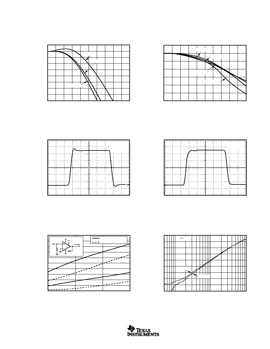
TYPICAL CHARACTERISTICS:
V
S
=
±
5V
T
A
= +25
°
C, G = +2, and R
L
= 100
(see Figure 1 for DC performance only), unless otherwise noted.
7
6
5
4
3
2
1
0
Frequency (25MHz/div)
0
250MHz
125MHz
LARGE-SIGNAL FREQUENCY RESPONSE
Gain (1dB/div)
V
O
= 1Vp-p
V
O
= 2Vp-p
V
O
= 7Vp-p
V
O
= 4Vp-p
400
300
200
100
0
100
200
300
400
SMALL-SIGNAL PULSE RESPONSE
Time (5ns/div)
Output Voltage (100mV/div)
V
O
= 0.5Vp-p
G = +2
0.20
0.18
0.16
0.14
0.12
0.10
0.08
0.06
0.04
0.02
0
Number of 150
Loads
1
2
3
4
COMPOSITE VIDEO dG/dP
dP
dP
dG
dG
dG/dP (%/
°
)
OPA692
Video In
Video Loads
5V
+5V
DIS
Optional
1.3k
Pull-Down
No Pull-Down
With 1.3k
Pull-Down
1
0
1
2
3
4
5
6
7
8
Frequency (50MHz/div)
0
500MHz
250MHz
SMALL-SIGNAL FREQUENCY RESPONSE
Normalized Gain (1dB/div)
G = +2
G = +1
G = 1
DISABLED FEEDTHROUGH vs FREQUENCY
50
55
60
65
70
75
80
85
90
95
Frequency (MHz)
1
0.5
10
100
Feedthrough (5dB/div)
V
DIS
= 0
Reverse
Forward
4
3
2
1
0
1
2
3
4
LARGE-SIGNAL PULSE RESPONSE
Time (5ns/div)
Output Voltage (1V/div)
V
O
= 5Vp-p
G = +2
OPA692
8
SBOS236C
www.ti.com
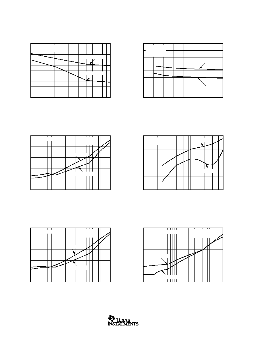
TYPICAL CHARACTERISTICS:
V
S
=
±
5V (Cont.)
T
A
= +25
°
C, G = +2, and R
L
= 100
(see Figure 1 for DC performance only), unless otherwise noted.
50
55
60
65
70
75
80
85
90
Supply Voltage (
±
V
S
)
2
2.5
3
3.5
4
4.5
5
5.5
6
5MHz HARMONIC DISTORTION vs SUPPLY VOLTAGE
Harmonic Distortion (dBc)
V
O
= 2Vp-p
R
L
= 100
f = 5MHz
2nd-Harmonic
3rd-Harmonic
60
65
70
75
80
85
90
95
100
105
110
Load Resistance (
)
100
1000
HARMONIC DISTORTION vs LOAD RESISTANCE
Harmonic Distortion (dBc)
V
O
= 2Vp-p
f = 5MHz
2nd-Harmonic
3rd-Harmonic
65
70
75
80
85
Output Voltage Swing (Vp-p)
0.1
1
5
HARMONIC DISTORTION vs OUTPUT VOLTAGE
Harmonic Distortion (dBc)
R
L
= 100
f = 5MHz
2nd-Harmonic
3rd-Harmonic
50
60
70
80
90
100
HARMONIC DISTORTION vs FREQUENCY (G = +2)
Frequency (MHz)
0.1
1
10
20
Harmonic Distortion (dBc)
dBc = dB Below Carrier
V
O
= 2Vp-p
R
L
= 100
3rd-Harmonic
2nd-Harmonic
50
60
70
80
90
100
HARMONIC DISTORTION vs FREQUENCY (G = 1)
Frequency (MHz)
0.1
1
10
20
Harmonic Distortion (dBc)
dBc = dB Below Carrier
V
O
= 2Vp-p
R
L
= 100
3rd-Harmonic
2nd-Harmonic
HARMONIC DISTORTION vs FREQUENCY (G = +1)
Frequency (MHz)
0.1
1
10
20
Harmonic Distortion (dBc)
50
60
70
80
90
100
dBc = dB Below Carrier
V
O
= 2Vp-p
R
L
= 100
2nd-Harmonic
3rd-Harmonic
OPA692
9
SBOS236C
www.ti.com
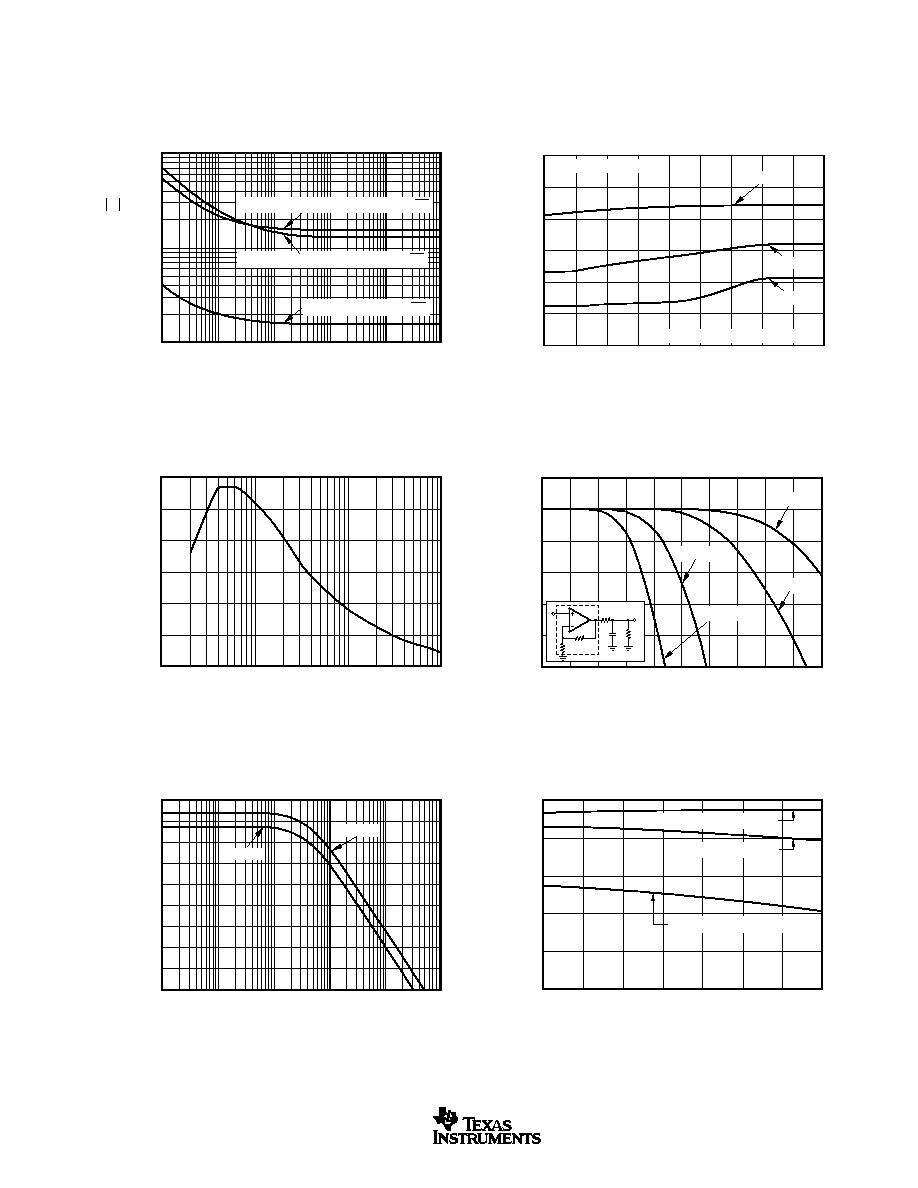
TYPICAL CHARACTERISTICS:
V
S
=
±
5V (Cont.)
T
A
= +25
°
C, G = +2, and R
L
= 100
(see Figure 1 for DC performance only), unless otherwise noted.
65
60
55
50
45
40
35
30
25
20
Frequency (Hz)
1k
10k
100k
1M
10M
100M
PSRR vs FREQUENCY
Power-Supply Rejection Ratio (dB)
+PSRR
PSRR
60
50
40
30
20
10
0
Capacitive Load (pF)
1
10
100
1k
RECOMMENDED R
S
vs CAPACITIVE LOAD
R
S
(
)
100
10
1
INPUT VOLTAGE AND CURRENT NOISE DENSITY
Frequency (Hz)
100
1k
10k
100k
1M
10M
Current Noise (pA/
Hz)
Voltage Noise (nV/
Hz)
Noninverting Current Noise (12pA/
Hz)
Inverting Input Current Noise (15pA/
Hz)
Voltage Noise (1.7nV/
Hz)
30
40
50
60
70
80
90
2-TONE, 3RD-ORDER
INTERMODULATION SPURIOUS
Single-Tone Load Power (dBm)
8
6
4
2
0
2
4
6
8
10
3rd-Order Spurious Level (dBc)
dBc = dB below carriers
50MHz
20MHz
10MHz
Load Power at Matched 50
Load
9
6
3
0
3
6
9
Frequency (25MHz/div)
0
250MHz
125MHz
FREQUENCY RESPONSE vs CAPACITIVE LOAD
Normalized Gain to Capacitive Load (dB)
OPA692
R
S
V
IN
V
O
C
L
1k
402
402
1k
is optional.
C
L
= 10pF
C
L
= 22pF
C
L
= 47pF
C
L
= 100pF
10
8
6
4
2
0
250
200
150
100
50
0
SUPPLY AND OUTPUT CURRENT vs TEMPERATURE
Ambient Temperature (
°
C)
50
25
0
25
50
75
100
125
Supply Current (2mA)
Output Current (50mA/div)
Quiescent Supply Current
Sinking Output Current
Sourcing Output Current
OPA692
10
SBOS236C
www.ti.com
TYPICAL CHARACTERISTICS:
V
S
=
±
5V (Cont.)
T
A
= +25
°
C, G = +2, and R
L
= 100
(see Figure 1 for DC performance only), unless otherwise noted.
2
1.5
1
0.5
0
0.5
1
1.5
2
TYPICAL DC DRIFT OVER TEMPERATURE
Ambient Temperature (
°
C)
50
25
0
25
50
75
100
125
Input Offset Voltage (mV)
40
30
20
10
0
10
20
30
40
Input Bias Currents (
µ
A)
Input Offset Voltage
Noninverting Input Bias Current
Inverting Input Bias Current
5
4
3
2
1
0
1
2
3
4
5
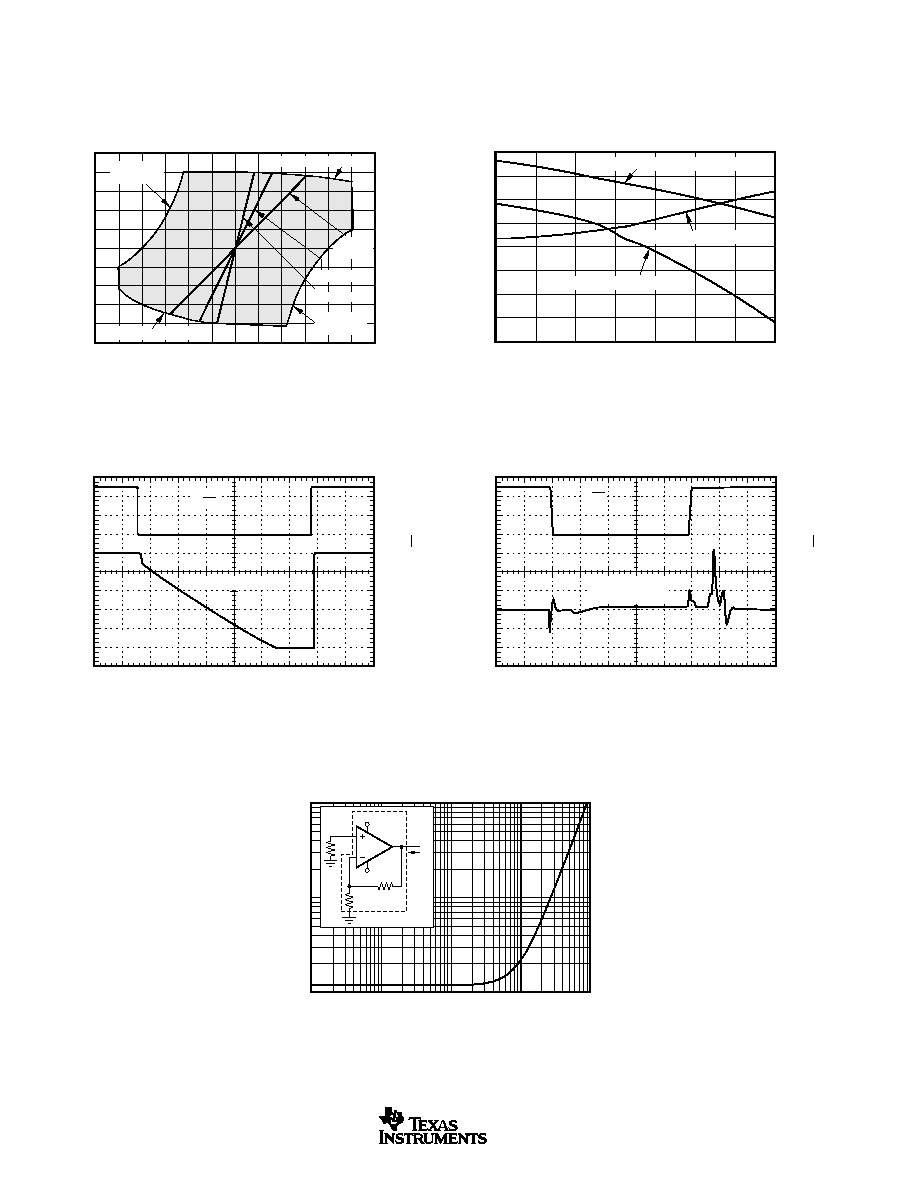
OUTPUT VOLTAGE AND CURRENT LIMITATIONS
I
O
(mA)
300 250 200 150 100 50
0
50
100 150 200 250 300
V
O
(V)
100
Load Line
50
Load Line
25
Load Line
Output Current Limited
1W Internal
Power Limit
1W Internal
Power Limit
Output Current Limit
LARGE-SIGNAL DISABLE/ENABLE RESPONSE
Output V
oltage (400mV/div)
Time (200ns/div)
2.0
1.6
1.2
0.8
0.4
0
V
DIS
(2V/div)
6.0
4.0
2.0
0
Output Voltage
V
DIS
V
IN
= +1V
DISABLE/ENABLE GLITCH
Output V
oltage (10mV/div)
Time (20ns/div)
30
20
10
0
10
20
V
DIS
(2V/div)
6.0
4.0
2.0
0
Output Voltage
(0V Input)
V
DIS
10
1
0.1
CLOSED-LOOP OUTPUT IMPEDANCE
Frequency (Hz)
10k
100M
100k
1M
10M
Output Impedance (
)
OPA692
402
+5V
5V
402
50
Z
O
OPA692
11
SBOS236C
www.ti.com
TYPICAL CHARACTERISTICS:
V
S
= +5V
T
A
= +25
°
C, G = +2, and R
L
= 100
(see Figure 2 for AC performance only), unless otherwise noted.
2.9
2.8
2.7
2.6
2.5
2.4
2.3
2.2
2.1
SMALL-SIGNAL PULSE RESPONSE
Time (5ns/div)
Output Voltage (100mV/div)
G = +2
V
O
= 0.5Vp-p
4.1
3.7
3.3
2.9
2.5
2.1
1.7
1.3
0.9
LARGE-SIGNAL PULSE RESPONSE
Time (5ns/div)
Output Voltage (400mV/div)
G = +2
V
O
= 2Vp-p
70
60
50
40
30
20
10
0
Capacitive Load (pF)
1
10
100
1k
RECOMMENDED R
S
vs CAPACITIVE LOAD
R
S
(
)
1
0
1
2
3
4
5
6
7
8
Frequency (Hz)
0
500M
250M
SMALL-SIGNAL FREQUENCY RESPONSE
Normalized Gain (1dB/div)
G = +1
G = +2
G = 1
7
6
5
4
3
2
1
0
Frequency (Hz)
0
250M
125M
LARGE-SIGNAL FREQUENCY RESPONSE
Gain (1dB/div)
R
L
= 100
to 2.5V
V
O
= 0.5Vp-p
V
O
= 2Vp-p
V
O
= 1Vp-p
9
6
3
0
3
6
9
FREQUENCY RESPONSE vs CAPACITIVE LOAD
Frequency (25MHz/div)
0
250MHz
125MHz
Normalized Gain to
Capacitive Load (dB)
OPA692
402
402
57.6
806
806
1k
V
IN
+5V
V
O
R
S
(1k
is optional)
C
L
0.1
µ
F
0.1
µ
F
C
L
= 10pF
C
L
= 22pF
C
L
= 47pF
C
L
= 100pF
OPA692
12
SBOS236C
www.ti.com
TYPICAL CHARACTERISTICS:
V
S
= +5V (Cont.)
T
A
= +25
°
C, G = +2, and R
L
= 100
(see Figure 2 for AC performance only), unless otherwise noted.
HARMONIC DISTORTION vs FREQUENCY
Frequency (MHz)
0.1
1
10
20
Harmonic Distortion (dBc)
50
60
70
80
90
V
O
= 2Vp-p
R
L
= 100
to 2.5V
2nd-Harmonic
3rd-Harmonic
30
35
40
45
50
55
60
65
70
75
80
Single-Tone Load Power (dBm)
14
12
10
8
6
4
2
0
2
2-TONE, 3RD-ORDER
INTERMODULATION SPURIOUS
3rd-Order Spurious Level (dBc)
dBc = dB Below Carriers
Load Power at Matched 50
Load
50MHz
20MHz
10MHz
HARMONIC DISTORTION vs OUTPUT VOLTAGE
Output Voltage Swing (Vp-p)
0.1
1
2
3
Harmonic Distortion (dBc)
60
65
70
75
80
R
L
= 100
to 2.5V
f = 5MHz
2nd-Harmonic
3rd-Harmonic
60
65
70
75
80
Load Resistance (
)
100
1k
HARMONIC DISTORTION vs LOAD RESISTANCE
Harmonic Distortion (dBc)
2nd-Harmonic
3rd-Harmonic
V
O
= 2Vp-p
f = 5MHz
OPA692
13
SBOS236C
www.ti.com
APPLICATIONS INFORMATION
WIDEBAND BUFFER OPERATION
The OPA692 gives the exceptional AC performance of a
wideband current-feedback op amp with a highly linear, high-
power output stage. It features internal R
F
and R
G
resistors
that make it easy to select a gain of +2, +1, or 1 without any
external resistors. Requiring only 5.1mA quiescent current, the
OPA692 will swing to within 1V of either supply rail and deliver
in excess of 160mA at room temperature. This low output
headroom requirement, along with supply voltage indepen-
dent biasing, gives remarkable single (+5V) supply operation.
The OPA692 will deliver greater than 200MHz bandwidth
driving a 2Vp-p output into 100
on a single +5V supply.
Previous boosted output stage amplifiers have typically suf-
fered from very poor crossover distortion as the output current
goes through zero. The OPA692 achieves a comparable
power gain with much better linearity. The primary advantage
of a current-feedback op amp over a voltage-feedback op amp
is that AC performance (bandwidth and distortion) is relatively
independent of signal gain.
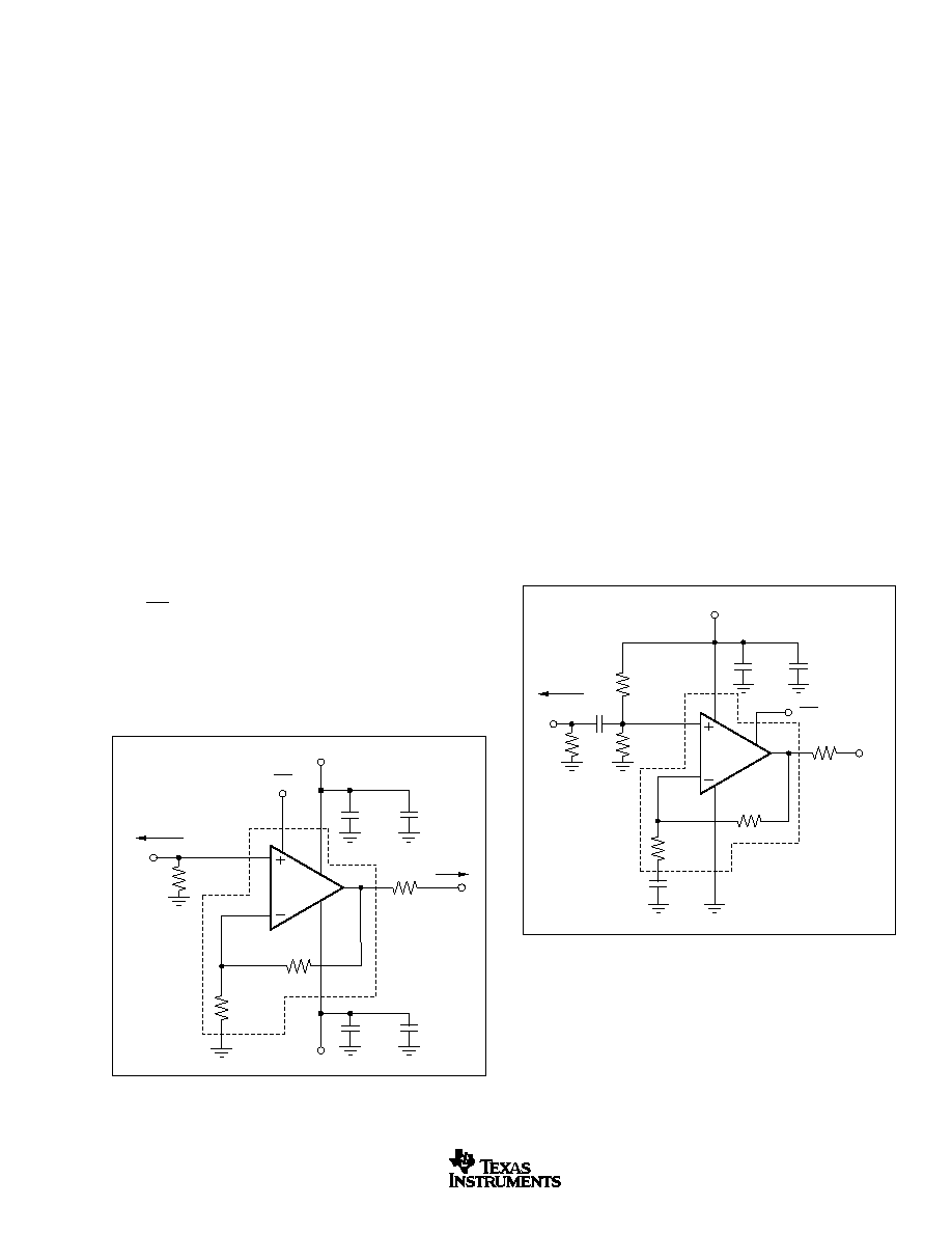
Figure 1 shows the DC-coupled, gain of +2, dual power-supply
circuit configuration used as the basis of the
±
5V Electrical and
Typical Characteristics. For test purposes, the input imped-
ance is set to 50
with a resistor to ground and the output
impedance is set to 50
with a series output resistor. Voltage
swings reported in the specifications are taken directly at the
input and output pins while load powers (dBm) are defined at
a matched 50
load. For the circuit of Figure 1, the total
effective load will be 100
|| 804
= 89
. The disable control
line (DIS) is typically left open to ensure normal amplifier
operation. In addition to the usual power-supply decoupling
capacitors to ground, a 0.1
µ
F capacitor can be included
between the two power-supply pins. This optional added
capacitor will typically improve the 2nd-harmonic distortion
performance by 3dB to 6dB.
Figure 2 shows the AC-coupled, gain of +2, single-supply
circuit configuration used as the basis of the +5V Electrical
and Typical Characteristics. Though not a
rail-to-rail design,
the OPA692 requires minimal input and output voltage head-
room compared to other very wideband current-feedback op
amps. It will deliver a 3Vp-p output swing on a single +5V
supply with greater than 150MHz bandwidth. The key re-
quirement of broadband single-supply operation is to main-
tain input and output signal swings within the usable voltage
ranges at both the input and the output. The circuit of Figure
2 establishes an input midpoint bias using a simple resistive
divider from the +5V supply (two 806
resistors). The input
signal is then AC-coupled into this midpoint voltage bias. The
input voltage can swing to within 1.5V of either supply pin,
giving a 2Vp-p input signal range centered between the
supply pins. The input impedance matching resistor (57.6
)
used for testing is adjusted to give a 50
input match when
the parallel combination of the biasing divider network is
included. The gain resistor (R
G
) is AC-coupled, giving the
circuit a DC gain of +1--which puts the input DC bias voltage
(2.5V) on the output as well. Again, on a single +5V supply,
the output voltage can swing to within 1V of either supply pin
while delivering more than 120mA output current. A demand-
ing 100
load to a midpoint bias is used in this characteriza-
tion circuit. The new output stage used in the OPA692 can
deliver large bipolar output currents into this midpoint load
with minimal crossover distortion, as shown by the +5V
supply, 3rd-harmonic distortion typical characteristics.
FIGURE 1. DC-Coupled, G = +2, Bipolar Supply, Specifica-
tion and Test Circuit.
FIGURE 2. AC-Coupled, G = +2, Single-Supply Specification
and Test Circuit.
OPA692
+5V
5V
50
Load
50
50
50
Source
R
G
402
R
F
402
+
6.8
µ
F
0.1
µ
F
+
6.8
µ
F
0.1
µ
F
DIS
V
IN
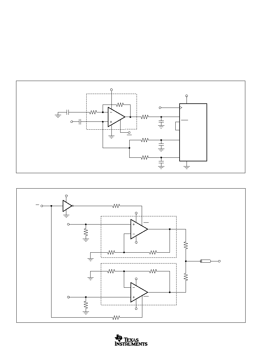
SINGLE-SUPPLY ADC INTERFACE
Most modern, high-performance ADCs (such as the Texas
Instruments ADS8xx and ADS9xx series) operate on a single
+5V (or lower) power supply. It has been a considerable
challenge for single-supply op amps to deliver a low-distor-
tion input signal at the ADC input for signal frequencies
OPA692
+5V
+V
S
DIS
V
S
/2
806
100
V
O
V
IN
806
R
G
402
R
F
402
0.1
µ
F
0.1
µ
F
+
6.8
µ
F
0.1
µ
F
50
Source
57.6
OPA692
14
SBOS236C
www.ti.com
exceeding 5MHz. The high slew rate, exceptional output
swing, and high linearity of the OPA692 make it an ideal
single-supply ADC driver. Figure 3 shows an example input
interface to a very high performance 10-bit, 60MSPS CMOS
converter.
The OPA692 in the circuit of Figure 3 provides 190MHz
bandwidth operating at a signal gain of +2 with a 2Vp-p output
swing. The noninverting input bias voltage is referenced to the
midpoint of the ADC signal range by dividing off the top and
bottom of the internal ADC reference ladder. With the gain
resistor (R
G
) AC-coupled, this bias voltage has a gain of +1 to
the output, centering the output voltage swing as well. Tested
performance at a 20MHz analog input frequency and a 60MSPS
clock rate on the converter gives > 58dBc SFDR.
WIDEBAND VIDEO MULTIPLEXING
One common application for video speed amplifiers that
include a disable pin is to wire multiple amplifier outputs
together, then select which one of several possible video
inputs to source onto a single line. This simple wired-OR
video multiplexer can be easily implemented using the
OPA692, as shown in Figure 4.
FIGURE 3. Wideband, AC-Coupled, Single-Supply ADC Driver.
FIGURE 4. 2-Channel Video Multiplexer.
OPA692
402
+2.5V DC Bias
ADS826
10-Bit
60MSPS
50
2Vp-p
DIS
22pF
Input
402
REFB
REFT
CM
Input
0.1
µ
F
0.1
µ
F
1Vp-p
2k
0.1
µ
F
+3.5V
2k
0.1
µ
F
+1.5V
+5V
Clock
+5V
R
G
R
F
OPA692
2k
V
OUT
75
Cable
RG-59
68.1
68.1
75
402
402
Video 1
+5V
+5V
|V
OUT
| < 2.6V
5V
OPA692
2k
75
402
402
Video 2
5V
+5V
V
DIS
DIS
DIS
OPA692
15
SBOS236C
www.ti.com
Typically, channel switching is performed either on sync or
retrace time in the video signal. The two inputs are approxi-
mately equal at this time. The
make-before-break disable
characteristic of the OPA692 ensures that there is always
one amplifier controlling the line when using a wired-OR
circuit (see Figure 4). Since both inputs may be on for a short
period during the transition between channels, the outputs
are combined through the output impedance matching resis-
tors (68.1
in this case). When one channel is disabled, its
feedback network forms part of the output impedance and
slightly attenuates the signal in getting out onto the cable.
The matching resistors have been set to get a signal gain of
+1 at the load while providing > 20dB return loss at the load.
The video multiplexer connection (see Figure 4) also insures
that the maximum differential voltage across the inputs of the
unselected channel do not exceed the rated
±
1.2V maximum
for standard video signal levels. In any case, V
OUT
must be
<
±
2.6Vp-p in order to not exceed the absolute maximum
differential input voltage (
±
1.2V) on the disabled channel.
The Disable Operation section shows the turn-on and turn-off
switching glitches using a grounded input for a single chan-
nel is typically less than
±
50mV. Where two outputs are
switched (see Figure 4), the output line is always under the
control of one amplifier or the other due to the make-before-
break disable timing. In this case, the switching glitches for
two 0V inputs drops to < 20mV.
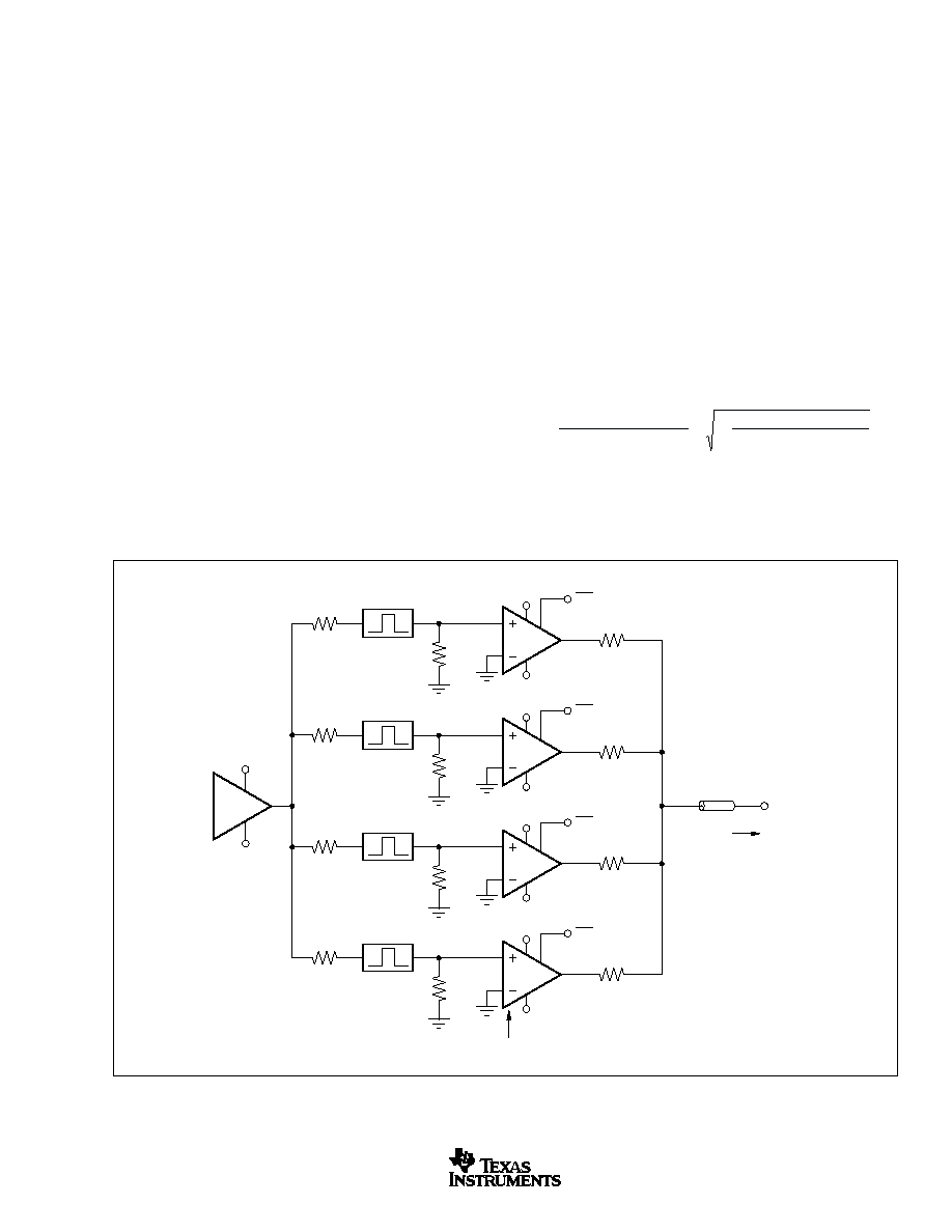
4-CHANNEL FREQUENCY CHANNELIZER
The circuit of Figure 5 is a 4-channel multiplexer. In this
circuit the OPA691 provides the drive for all four channels.
Each channel includes a bandpass filter and each bandpass
filter is set for a different frequency band. This allows the
channelizing part of this circuit. The role of the OPA692 is to
provide impedance isolation. This is done through the use of
four matching resistances (59
in this case). These match-
ing resistors ensure that the signals will combine during the
transition between channels. They have been used to get a
gain of +1 at the load.
This circuit may be used with a different number of channels.
Its limitation comes from the drive requirement for each
channel, as well as the minimum acceptable return loss.
The output resistor value (R
O
) to keep a gain of +1 at the
load, depends on the number of channels. For the OPA692,
Equation 1 gives:
(1)
R
n
n
O
=
·
(
)
+
[
]
·
+
· -
(
)
+
[
]
75
2
804
2
1
241200
75
2
804
1
2
Where n = number of devices in multiplexer.
OPA692
V
OUT
75
Cable
75
Load
RG-59
75
OPA691
75
R
O
59
R
O
59
R
O
59
R
O
59
#1
DIS 1
OPA692
75
75
#2
DIS 2
OPA692
75
75
#3
DIS 3
+5V
5V
+5V
5V
+5V
5V
+5V
5V
+5V
5V
G = +2 Stages
OPA692
75
75
#4
DIS 4
FIGURE 5. 4-Channel Frequency Channelizer.
OPA692
16
SBOS236C
www.ti.com
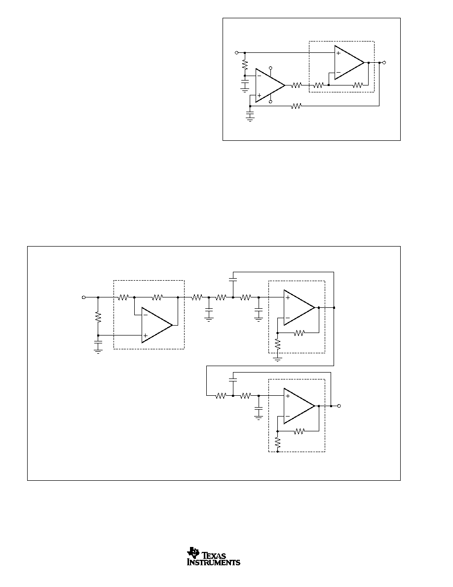
DELAY-EQUALIZED LOW-PASS FILTER
The circuit in Figure 6 realizes a 5th-order Butterworth low-
pass filter with a 3dB bandwidth of 20MHz and group delay
equalization. This filter is based on the KRC active filter
topology using amplifiers with a fixed positive gain
1.
The OPA692 makes a good amplifier for this type of filter. The
first stage is the group delay equalizer, which is based on a
gain of 1. The second stage has a high-Q pole, uses a gain
of +2 for minimum component sensitivity, and also produces a
real pole. The last stage has a low-Q pole, and uses a gain of
+1 for minimum component sensitivity.
The component values have been predistorted to compensate
for the op amps parasitic effects. The low-Q pole section was
placed last to minimize noise peaking in the passband, while
maintaining good dynamic range performance.
PRECISION VOLTAGE BUFFER
The precision buffer in Figure 7 combines the DC precision
and low 1/f noise of the OPA227 with the high-speed perfor-
mance of the OPA692. The 80.6k
resistor makes the high-
frequency and low-frequency nominal gains equal. The
OPA692 takes over from the OPA227 at approximately 32kHz.
OPA692
115
402
49.9
105
226
402
100pF
220pF
56pF
27pF
V
IN
V
OUT
OPA692
402
402
95.3
226
68pF
39pF
OPA692
402
402
(Open)
FIGURE 7. Precision Wideband, Unity-Gain Buffer.
OPA227
OPA692
402
402
80.6k
200
V
IN
V
OUT
5V
+5V
200
2.7nF
2.7nF
FIGURE 6. Butterworth LP Filter with Delay Equalization.
DESIGN-IN TOOLS
DEMONSTRATION BOARDS
Two PC boards are available to assist in the initial evaluation
of circuit performance using the OPA692 in its two package
styles. All of these are available free as an unpopulated PC

OPA692
17
SBOS236C
www.ti.com
board delivered with descriptive documentation. The sum-
mary information for these boards is shown in the table
below.
over-temperature specifications because the output stage
junction temperatures are higher than the minimum specified
operating ambient.
DRIVING CAPACITIVE LOADS
One of the most demanding and yet very common load
conditions for an op amp is capacitive loading. Often, the
capacitive load is the input of an ADC--including additional
external capacitance which may be recommended to improve
ADC linearity. A high-speed amplifier like the OPA692 can be
very susceptible to decreased stability and frequency re-
sponse peaking when a capacitive load is placed directly on
the output pin. When the amplifier's open-loop output resis-
tance is considered, this capacitive load introduces an addi-
tional pole in the signal path that can decrease the phase
margin. Several external solutions to this problem have been
suggested. When the primary considerations are frequency
response flatness, pulse response fidelity, and/or distortion,
the simplest and most effective solution is to isolate the
capacitive load from the feedback loop by inserting a series
isolation resistor between the amplifier output and the capaci-
tive load. This does not eliminate the pole from the loop
response, but rather shifts it and adds a zero at a higher
frequency. The additional zero acts to cancel the phase lag
from the capacitive load pole, thus increasing the phase
margin and improving stability.
The Typical Characteristics show the recommended "R
S
vs
Capacitive Load" and the resulting frequency response at the
load. Parasitic capacitive loads greater than 2pF can begin to
degrade the performance of the OPA692. Long PC board
traces, unmatched cables, and connections to multiple de-
vices can easily cause this value to be exceeded. Always
consider this effect carefully, and add the recommended
series resistor as close as possible to the OPA692 output pin
(see the Board Layout Guidelines section).
DISTORTION PERFORMANCE
The OPA692 provides good distortion performance into a
100
load on
±
5V supplies. Relative to alternative solutions, it
provides exceptional performance into lighter loads and/or
operating on a single +5V supply. Generally, until the funda-
mental signal reaches very high-frequency or power levels, the
2nd-harmonic will dominate the distortion with a negligible 3rd-
harmonic component. Focusing then on the 2nd-harmonic,
increasing the load impedance improves distortion directly.
Remember that the total load includes the feedback network--
in the noninverting configuration (see Figure 1) this is the sum
of R
F
+ R
G
, while in the inverting configuration, it is just R
F
.
Also, providing an additional supply decoupling capacitor
(0.1
µ
F) between the supply pins (for bipolar operation) im-
proves the 2nd-order distortion slightly (3dB to 6dB).
In most op amps, increasing the output voltage swing increases
harmonic distortion directly. The Typical Characteristics show the
2nd-harmonic increasing at a little less than the expected 2x rate
while the 3rd-harmonic increases at a much lower rate than the
expected 3x. Where the test power doubles, the difference
between it and the 2nd-harmonic decreases less than the
BOARD
LITERATURE
PART
REQUEST
PRODUCT
PACKAGE
NUMBER
NUMBER
OPA692ID
SO-8
DEM-OPA68xU
SBOU009
OPA692IDBV
SOT23-6
DEM-OPA6xxN
SBOU010
To request any of these boards, check the Texas Instruments
web site at www.ti.com.
OPERATING SUGGESTIONS
GAIN SETTING
Setting the gain with the OPA692 is very easy. For a gain of
+2, ground the IN pin and drive the +IN pin with the signal.
For a gain of +1, leave the IN pin open and drive the +IN pin
with the signal. For a gain of 1, ground the +IN pin and drive
the IN pin with the signal. As the internal resistor values (not
their ratio) change over temperature and process, external
resistors should not be used to modify the gain.
OUTPUT CURRENT AND VOLTAGE
The OPA692 provides output voltage and current capabilities
that are unsurpassed in a low-cost monolithic op amp. Under
no-load conditions at +25
°
C, the output voltage typically
swings closer than 1V to either supply rail; the tested swing
limit is within 1.2V of either rail. Into a 15
load (the minimum
tested load), it is specified to deliver more than
±
160mA.
The specifications described previously, though familiar in
the industry, consider voltage and current limits separately. In
many applications, it is the voltage times current, or V-I
product, which is more relevant to circuit operation. Refer to
the "Output Voltage and Current Limitations" plot in the
Typical Characteristics. The X- and Y-axes of this graph show
the zero-voltage output current limit and the zero-current
output voltage limit, respectively. The four quadrants give a
more detailed view of the OPA692 output drive capabilities,
noting that the graph is bounded by a safe operating area of
1W maximum internal power dissipation. Superimposing
resistor load lines onto the plot shows that the OPA692 can
drive
±
2.5V into 25
, or
±
3.5V into 50
without exceeding
the output capabilities or the 1W dissipation limit. A 100
load line (the standard test circuit load) shows the full
±
3.9V
output swing capability (see the Electrical Characteristics).
The minimum specified output voltage and current over
temperature are set by worst-case simulations at the cold
temperature extreme. Only at cold startup will the output
current and voltage decrease to the numbers shown in the
Electrical Characteristics. As the output transistors deliver
power, their junction temperatures increase, decreasing their
V
BE
s (increasing the available output voltage swing), and
increasing their current gains (increasing the available output
current). In steady-state operation, the available output volt-
age and current is always greater than that shown in the
OPA692
18
SBOS236C
www.ti.com
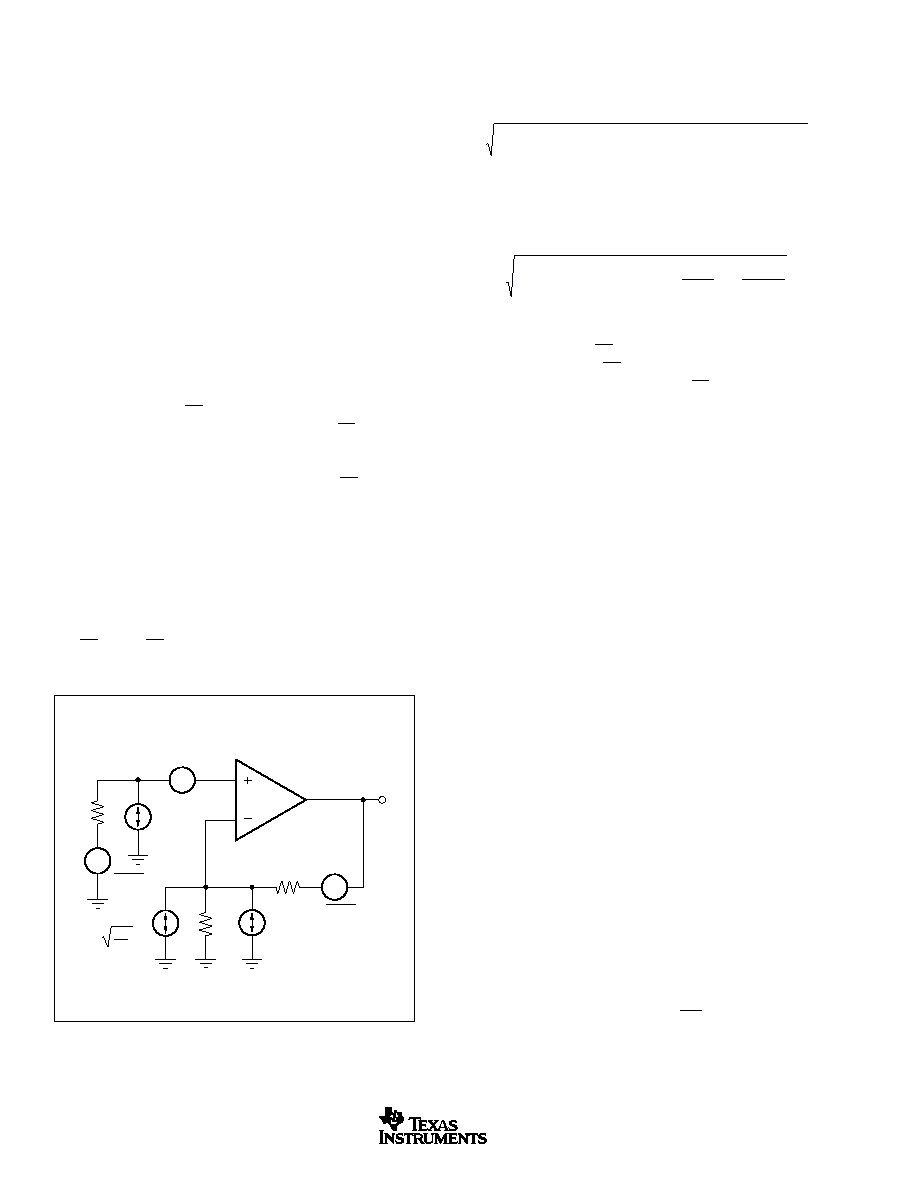
FIGURE 8. Noise Model.
expected 6dB, while the difference between it and the 3rd
decreases by less than the expected 12dB. This also shows up
in the 2-tone, 3rd-order intermodulation spurious (IM3) response
curves. The 3rd-order spurious levels are extremely low at low
output power levels. The output stage continues to hold them low
even as the fundamental power reaches very high levels. As the
Typical Characteristics show, the spurious intermodulation pow-
ers do not increase as predicted by a traditional intercept model.
As the fundamental power level increases, the dynamic range
does not decrease significantly. For two tones centered at
20MHz, with 10dBm/tone into a matched 50
load (i.e., 2Vp-p
for each tone at the load, which requires 8Vp-p for the overall
2-tone envelope at the output pin), the Typical Characteristics
show 58dBc difference between the test-tone power and the 3rd-
order intermodulation spurious levels. This exceptional perfor-
mance improves further when operating at lower frequencies.
NOISE PERFORMANCE
The OPA692 offers an excellent balance between voltage and
current noise terms to achieve low output noise. The inverting
current noise (15pA/
Hz) is significantly lower than earlier
solutions while the input voltage noise (1.7nV
Hz) is lower
than most unity-gain stable, wideband, voltage-feedback op
amps. This low input voltage noise was achieved at the price
of higher noninverting input current noise (12pA/
Hz). As long
as the AC source impedance looking out of the noninverting
node is less than 100
, this current noise will not contribute
significantly to the total output noise. The op amp input voltage
noise and the two input current noise terms combine to give
low output noise for the gain settings, available using the
OPA692. Figure 8 shows the op amp noise analysis model
with all the noise terms included. In this model, all noise terms
are taken to be noise voltage or current density terms in either
nV/
Hz or pA/
Hz.
The total output spot noise voltage can be computed as the
square root of the sum of all squared output noise voltage
contributors. Equation 2 shows the general form for the output
noise voltage using the terms shown in Figure 8.
(2)
E
E
I
R
kTR
NG
I R
kTR NG
O
NI
BN S
S
BI F
F
=
+
(
)
+
+
(
)
+
2
2
2
2
4
4
Dividing this expression by the noise gain (NG = (1 + R
F
/R
G
))
will give the equivalent input-referred spot noise voltage at the
noninverting input, as shown in Equation 3.
(3)
E
E
I
R
kTR
I R
NG
kTR
NG
N
NI
BN S
S
BI F
F
=
+
(
)
+
+
+
2
2
2
4
4
Evaluating these two equations for the OPA692 circuit and
component values (see Figure 1) will give a total output spot
noise voltage of 8.2nV/
Hz and a total equivalent input spot
noise voltage of 4.1nV/
Hz. This total input-referred spot
noise voltage is higher than the 1.7nV/
Hz specification for
the op amp voltage noise alone. This reflects the noise added
to the output by the inverting current noise times the feed-
back resistor.
DC ACCURACY
The OPA692 provides exceptional bandwidth in high gains,
giving fast pulse settling but only moderate DC accuracy. The
Electrical Characteristics show an input offset voltage com-
parable to high-speed voltage-feedback amplifiers. However,
the two input bias currents are somewhat higher and are
unmatched. Bias current cancellation techniques will not
reduce the output DC offset for OPA692. As the two input
bias currents are unrelated in both magnitude and polarity,
matching the source impedance looking out of each input to
reduce their error contribution to the output is ineffective.
Evaluating the configuration of Figure 1, using worst-case
+25
°
C input offset voltage and the two input bias currents,
gives a worst-case output offset range equal to:
±
(NG · V
OS
(max)) + (I
BN
· R
S
/2 · NG)
±
(I
BI
· R
F
)
where NG = noninverting signal gain
=
±
(2 · 2.5mV) + (35
µ
A · 25
· 2)
±
(402
· 25
µ
A)
=
±
5mV + 1.75mV
±
10.05mV
= 13.3mV
+16.80mV
Minimizing the resistance seen by the noninverting input will
give the best DC offset performance.
For significantly improved DC accuracy, consider the preci-
sion buffer circuit (see Figure 7).
DISABLE OPERATION
The OPA692 provides an optional disable feature that may be
used either to reduce system power or to implement a simple
channel multiplexing operation. If the DIS control pin is left
unconnected, the OPA692 will operate normally. To disable,
4kT
R
G
R
G
R
F
R
S
OPA692
I
BI
E
O
I
BN
4kT = 1.6E 20J
at 290
°
K
E
RS
E
NI
4kTR
S
4kTR
F
OPA692
19
SBOS236C
www.ti.com
the control pin must be asserted LOW. Figure 9 shows a
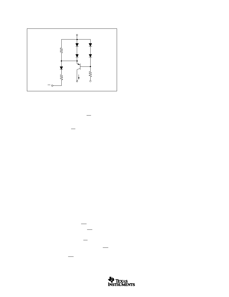
simplified internal circuit for the disable control feature.
In normal operation, base current to Q1 is provided through
THERMAL ANALYSIS
Due to the high output power capability of the OPA692,
heatsinking or forced airflow may be required under extreme
operating conditions. Maximum desired junction temperature
will set the maximum allowed internal power dissipation, as
described below. In no case should the maximum junction
temperature be allowed to exceed 175
°
C.
Operating junction temperature (T
J
) is given by T
A
+ P
D
·
JA
.
The total internal power dissipation (P
D
) is the sum of
quiescent power (P
DQ
) and additional power dissipated in the
output stage (P
DL
) to deliver load power. Quiescent power is
simply the specified no-load supply current times the total
supply voltage across the part. P
DL
depends on the required
output signal and load but would, for a grounded resistive
load, be at a maximum when the output is fixed at a voltage
equal to 1/2 either supply voltage (for equal bipolar supplies).
Under this condition P
DL
= V
S
2
/(4 · R
L
), where R
L
includes
feedback network loading.
Note that it is the power in the output stage and not in the
load that determines internal power dissipation.
As a worst-case example, compute the maximum T
J
using an
OPA692IDBV (SOT23-6 package) in the circuit of Figure 1
operating at the maximum specified ambient temperature of
+85
°
C and driving a grounded 20
load to +2.5V
DC
:
P
D
= 10V · 5.8mA + 5
2
/(4 · (20
|| 800
)) = 378mW
Maximum T
J
= +85
°
C + (0.39W · 150
°
C/W) = 142
°
C
Although this is still well below the specified maximum
junction temperature, system reliability considerations may
require lower junction temperatures. Remember, this is a
worst-case internal power dissipation--use your actual sig-
nal and load to compute P
DL
. The highest possible internal
dissipation occurs if the load requires current to be forced
into the output for positive output voltages or sourced from
the output for negative output voltages. This puts a high
current through a large internal voltage drop in the output
transistors. The "Output Voltage and Current Limitations" plot
shown in the Typical Characteristics include a boundary for
1W maximum internal power dissipation under these condi-
tions.
BOARD LAYOUT GUIDELINES
Achieving optimum performance with a high-frequency am-
plifier like the OPA692 requires careful attention to board
layout parasitics and external component types. Recommen-
dations that will optimize performance include:
a) Minimize parasitic capacitance to any AC ground for
all of the signal I/O pins. Parasitic capacitance on the
output pin can cause instability: on the noninverting input, it
can react with the source impedance to cause unintentional
bandlimiting. To reduce unwanted capacitance, a window
around the signal I/O pins should be opened in all of the
ground and power planes around those pins. Otherwise,
ground and power planes should be unbroken elsewhere on
the board.
the 110k
resistor while the emitter current through the 15k
resistor sets up a voltage drop that is inadequate to turn on
the two diodes in Q1's emitter. As V
DIS
is pulled LOW,
additional current is pulled through the 15k
resistor eventu-
ally turning on these two diodes (
75
µ
A). At this point, any
further current pulled out of V
DIS
goes through those diodes
holding the emitter-base voltage of Q1 at approximately 0V.
This shuts off the collector current out of Q1, turning the
amplifier off. The supply current in the disable mode is only
that required to operate the circuit of Figure 8. Additional
circuitry ensures that turn-on time occurs faster than turn-off
time (make-before-break).
When disabled, the output and input nodes go to a high-
impedance state. If the OPA692 is operating in a gain of +1,
this will show a very high impedance (4pF || 1M
) at the
output and exceptional signal isolation. If operating at a gain
of +2, the total feedback network resistance (R
F
+ R
G
) will
appear as the impedance looking back into the output, but
the circuit will still show very high forward and reverse
isolation. If configured at a gain of 1, the input and output
will be connected through the feedback network resistance
(R
F
+ R
G
) giving relatively poor input to output isolation.
One key parameter in disable operation is the output glitch
when switching in and out of the disabled mode. The Typical
Characteristics show these glitches for the circuit of Figure 1
with the input signal set to 0V. The glitch waveform at the
output pin is plotted along with the DIS pin voltage.
The transition edge rate (dV/dt) of the DIS control line will
influence this glitch. Slowing this edge can be achieved by
adding a simple RC filter into the V
DIS
pin from a higher
speed logic line. If extremely fast transition logic is used, a
2k
series resistor between the logic gate and the DIS input
pin will provide adequate bandlimiting using just the parasitic
input capacitance on the DIS pin while still ensuring an
adequate logic level swing.
25k
110k
15k
I
S
Control
V
S
+V
S
V
DIS
Q1
FIGURE 9. Simplified Disable Control Circuit.
OPA692
20
SBOS236C
www.ti.com
External
Pin
+V
CC
V
CC
Internal
Circuitry
b) Minimize the distance (< 0.25") from the power-supply
pins to high-frequency 0.1
µ
F decoupling capacitors. At
the device pins, the ground and power-plane layout should
not be in close proximity to the signal I/O pins. Avoid narrow
power and ground traces to minimize inductance between
the pins and the decoupling capacitors. The power-supply
connections (on pins 4 and 7) should always be decoupled
with these capacitors. An optional supply decoupling capaci-
tor across the two power supplies (for bipolar operation) will
improve 2nd-harmonic distortion performance. Larger (2.2
µ
F
to 6.8
µ
F) decoupling capacitors, effective at lower frequen-
cies, should also be used on the main supply pins. These
may be placed somewhat further from the device and may be
shared among several devices in the same area of the PC
board.
c) Careful selection and placement of external compo-
nents will preserve the high-frequency performance of
the OPA692. Any external resistors should be a very low
reactance type. Surface-mount resistors work best and allow
a tighter overall layout. Metal-film and carbon composition,
axially-leaded resistors can also provide good high-frequency
performance. Again, keep their leads and PC-board trace
length as short as possible. Never use wirewound type
resistors in a high-frequency application. All external compo-
nents should also be placed close to the package.
d) Connections to other wideband devices on the board
may be made with short direct traces or through onboard
transmission lines. For short connections, consider the
trace and the input to the next device as a lumped capacitive
load. Relatively wide traces (50mils to 100mils) should be
used, preferably with ground and power planes opened up
around them. Estimate the total capacitive load and set R
S
from the plot of recommended "R
S
vs Capacitive Load." Low
parasitic capacitive loads (< 5pF) may not need an R
S
because the OPA692 is nominally compensated to operate
with a 2pF parasitic load. If a long trace is required, and the
6dB signal loss intrinsic to a doubly-terminated transmission
line is acceptable, implement a matched impedance trans-
mission line using microstrip or stripline techniques (consult
an ECL design handbook for microstrip and stripline layout
techniques). A 50
environment is normally not necessary
on board, and in fact, a higher impedance environment will
improve distortion as shown in the "Distortion vs Load" plots.
With a characteristic board trace impedance defined based
on board material and trace dimensions, a matching series
resistor into the trace from the output of the OPA692 is used
as well as a terminating shunt resistor at the input of the
destination device. Remember also that the terminating im-
pedance will be the parallel combination of the shunt resistor
and the input impedance of the destination device; this total
effective impedance should be set to match the trace imped-
ance. The high output voltage and current capability of the
OPA692 allows multiple destination devices to be handled as
separate transmission lines, each with their own series and
shunt terminations. If the 6dB attenuation of a doubly-termi-
nated transmission line is unacceptable, a long trace can be
series-terminated at the source end only. Treat the trace as
a capacitive load in this case and set the series resistor value
as shown in the plot of "R
S
vs Capacitive Load." This will not
preserve signal integrity as well as a doubly-terminated line.
If the input impedance of the destination device is low, there
will be some signal attenuation due to the voltage divider
formed by the series output into the terminating impedance.
e) Socketing a high-speed part like the OPA692 is not
recommended. The additional lead length and pin-to-pin
capacitance introduced by the socket can create an ex-
tremely troublesome parasitic network which can make it
almost impossible to achieve a smooth, stable frequency
response. Best results are obtained by soldering the OPA692
onto the board.
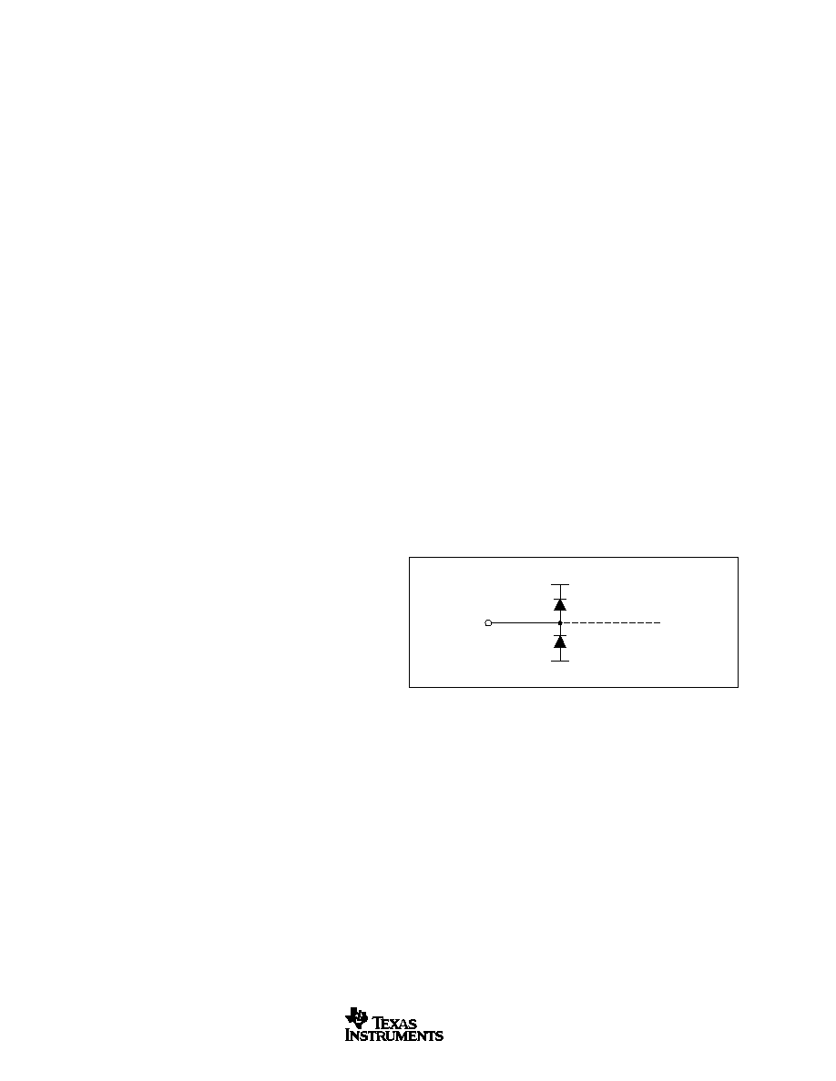
INPUT AND ESD PROTECTION
The OPA692 is built using a very high-speed complementary
bipolar process. The internal junction breakdown voltages
are relatively low for these very small geometry devices.
These breakdowns are reflected in the Absolute Maximum
Ratings table. All device pins have limited ESD protection
using internal diodes to the power supplies, as shown in
Figure 10.
FIGURE 10. Internal ESD Protection.
These diodes provide moderate protection to input overdrive
voltages above the supplies as well. The protection diodes
can typically support 30mA continuous current. Where higher
currents are possible (e.g., in systems with
±
15V supply parts
driving into the OPA692), current-limiting series resistors
should be added into the two inputs. Keep these resistor
values as low as possible since high values degrade both
noise performance and frequency response.
OPA692
21
SBOS236C
www.ti.com
PACKAGE DRAWINGS
D (R-PDSO-G**)
PLASTIC SMALL-OUTLINE PACKAGE
8 PINS SHOWN
8
0.197
(5,00)
A MAX
A MIN
(4,80)
0.189
0.337
(8,55)
(8,75)
0.344
14
0.386
(9,80)
(10,00)
0.394
16
DIM
PINS **
4040047/E 09/01
0.069 (1,75) MAX
Seating Plane
0.004 (0,10)
0.010 (0,25)
0.010 (0,25)
0.016 (0,40)
0.044 (1,12)
0.244 (6,20)
0.228 (5,80)
0.020 (0,51)
0.014 (0,35)
1
4
8
5
0.150 (3,81)
0.157 (4,00)
0.008 (0,20) NOM
0
°
8
°
Gage Plane
A
0.004 (0,10)
0.010 (0,25)
0.050 (1,27)
NOTES: A. All linear dimensions are in inches (millimeters).
B. This drawing is subject to change without notice.
C. Body dimensions do not include mold flash or protrusion, not to exceed 0.006 (0,15).
D. Falls within JEDEC MS-012
OPA692
22
SBOS236C
www.ti.com
PACKAGE DRAWINGS
(Cont.)
DBV (R-PDSO-G6)
PLASTIC SMALL-OUTLINE
0,10
M
0,20
0,95
0 8
0,25
0,55
0,35
Gage Plane
0,15 NOM
4073253-5/G 01/02
2,60
3,00
0,50
0,25
1,50
1,70
4
6
3
1
2,80
3,00
1,45
0,95
0,05 MIN
Seating Plane
6X
NOTES: A. All linear dimensions are in millimeters.
B. This drawing is subject to change without notice.
C. Body dimensions do not include mold flash or protrusion.
D. Leads 1, 2, 3 may be wider than leads 4, 5, 6 for package orientation.

PACKAGING INFORMATION
Orderable Device
Status
(1)
Package
Type
Package
Drawing
Pins Package
Qty
Eco Plan
(2)
Lead/Ball Finish
MSL Peak Temp
(3)
OPA692ID
ACTIVE
SOIC
D
8
100
None
CU NIPDAU
Level-3-240C-168 HR
OPA692IDBVR
ACTIVE
SOT-23
DBV
6
3000
None
CU NIPDAU
Level-3-235C-168 HR
OPA692IDBVT
ACTIVE
SOT-23
DBV
6
250
None
CU NIPDAU
Level-3-235C-168 HR
OPA692IDR
ACTIVE
SOIC
D
8
2500
None
CU NIPDAU
Level-3-240C-168 HR
(1)
The marketing status values are defined as follows:
ACTIVE: Product device recommended for new designs.
LIFEBUY: TI has announced that the device will be discontinued, and a lifetime-buy period is in effect.
NRND: Not recommended for new designs. Device is in production to support existing customers, but TI does not recommend using this part in
a new design.
PREVIEW: Device has been announced but is not in production. Samples may or may not be available.
OBSOLETE: TI has discontinued the production of the device.
(2)
Eco Plan - May not be currently available - please check
http://www.ti.com/productcontent
for the latest availability information and additional
product content details.
None: Not yet available Lead (Pb-Free).
Pb-Free (RoHS): TI's terms "Lead-Free" or "Pb-Free" mean semiconductor products that are compatible with the current RoHS requirements
for all 6 substances, including the requirement that lead not exceed 0.1% by weight in homogeneous materials. Where designed to be soldered
at high temperatures, TI Pb-Free products are suitable for use in specified lead-free processes.
Green (RoHS & no Sb/Br): TI defines "Green" to mean "Pb-Free" and in addition, uses package materials that do not contain halogens,
including bromine (Br) or antimony (Sb) above 0.1% of total product weight.
(3)
MSL, Peak Temp. -- The Moisture Sensitivity Level rating according to the JEDECindustry standard classifications, and peak solder
temperature.
Important Information and Disclaimer:The information provided on this page represents TI's knowledge and belief as of the date that it is
provided. TI bases its knowledge and belief on information provided by third parties, and makes no representation or warranty as to the
accuracy of such information. Efforts are underway to better integrate information from third parties. TI has taken and continues to take
reasonable steps to provide representative and accurate information but may not have conducted destructive testing or chemical analysis on
incoming materials and chemicals. TI and TI suppliers consider certain information to be proprietary, and thus CAS numbers and other limited
information may not be available for release.
In no event shall TI's liability arising out of such information exceed the total purchase price of the TI part(s) at issue in this document sold by TI
to Customer on an annual basis.
PACKAGE OPTION ADDENDUM
www.ti.com
1-Feb-2005
Addendum-Page 1
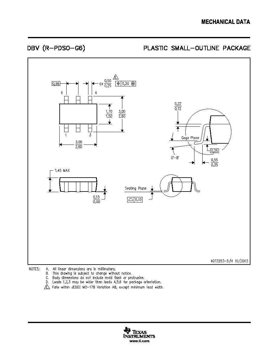
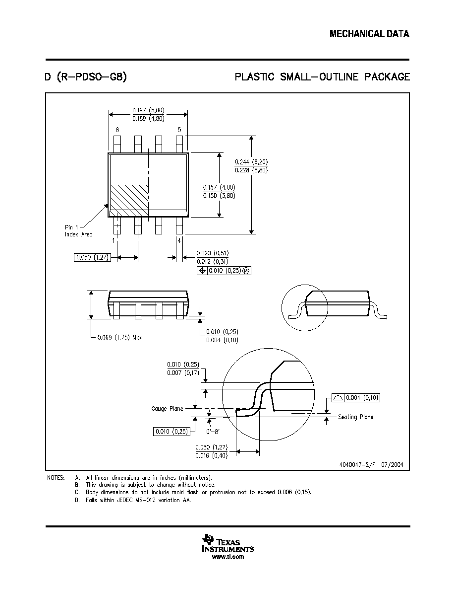

IMPORTANT NOTICE
Texas Instruments Incorporated and its subsidiaries (TI) reserve the right to make corrections, modifications,
enhancements, improvements, and other changes to its products and services at any time and to discontinue
any product or service without notice. Customers should obtain the latest relevant information before placing
orders and should verify that such information is current and complete. All products are sold subject to TI's terms
and conditions of sale supplied at the time of order acknowledgment.
TI warrants performance of its hardware products to the specifications applicable at the time of sale in
accordance with TI's standard warranty. Testing and other quality control techniques are used to the extent TI
deems necessary to support this warranty. Except where mandated by government requirements, testing of all
parameters of each product is not necessarily performed.
TI assumes no liability for applications assistance or customer product design. Customers are responsible for
their products and applications using TI components. To minimize the risks associated with customer products
and applications, customers should provide adequate design and operating safeguards.
TI does not warrant or represent that any license, either express or implied, is granted under any TI patent right,
copyright, mask work right, or other TI intellectual property right relating to any combination, machine, or process
in which TI products or services are used. Information published by TI regarding third-party products or services
does not constitute a license from TI to use such products or services or a warranty or endorsement thereof.
Use of such information may require a license from a third party under the patents or other intellectual property
of the third party, or a license from TI under the patents or other intellectual property of TI.
Reproduction of information in TI data books or data sheets is permissible only if reproduction is without
alteration and is accompanied by all associated warranties, conditions, limitations, and notices. Reproduction
of this information with alteration is an unfair and deceptive business practice. TI is not responsible or liable for
such altered documentation.
Resale of TI products or services with statements different from or beyond the parameters stated by TI for that
product or service voids all express and any implied warranties for the associated TI product or service and
is an unfair and deceptive business practice. TI is not responsible or liable for any such statements.
Following are URLs where you can obtain information on other Texas Instruments products and application
solutions:
Products
Applications
Amplifiers
amplifier.ti.com
Audio
www.ti.com/audio
Data Converters
dataconverter.ti.com
Automotive
www.ti.com/automotive
DSP
dsp.ti.com
Broadband
www.ti.com/broadband
Interface
interface.ti.com
Digital Control
www.ti.com/digitalcontrol
Logic
logic.ti.com
Military
www.ti.com/military
Power Mgmt
power.ti.com
Optical Networking
www.ti.com/opticalnetwork
Microcontrollers
microcontroller.ti.com
Security
www.ti.com/security
Telephony
www.ti.com/telephony
Video & Imaging
www.ti.com/video
Wireless
www.ti.com/wireless
Mailing Address:
Texas Instruments
Post Office Box 655303 Dallas, Texas 75265
Copyright
2005, Texas Instruments Incorporated
Document Outline
- FEATURES
- APPLICATIONS
- DESCRIPTION
- ABSOLUTE MAXIMUM RATINGS
- PACKAGE/ORDERING INFORMATION
- PIN CONFIGURATION
- ELECTRICAL CHARACTERISTICS: V S =±5V
- ELECTRICAL CHARACTERISTICS: V S =+5V
- TYPICAL CHARACTERISTICS: V S =±5V
- TYPICAL CHARACTERISTICS: V S =+5V
- APPLICATIONS INFORMATION
- WIDEBAND BUFFER OPERATION
- SINGLE-SUPPLY ADC INTERFACE
- WIDEBAND VIDEO MULTIPLEXING
- 4-CHANNEL FREQUENCY CHANNELIZER
- DELAY-EQUALIZED LOW-PASS FILTER
- PRECISION VOLTAGE BUFFER
- DESIGN-IN TOOLS
- OPERATING SUGGESTIONS
- GAIN SETTING
- OUTPUT CURRENT AND VOLTAGE
- DRIVING CAPACITIVE LOADS
- DISTORTION PERFORMANCE
- NOISE PERFORMANCE
- DC ACCURACY
- DISABLE OPERATION
- THERMAL ANALYSIS
- BOARD LAYOUT GUIDELINES
- INPUT AND ESD PROTECTION
- PACKAGE DRAWINGS
- D (R-PDSO-G**) PLASTIC SMALL-OUTLINE PACKAGE
- DBV (R-PDSO-G6) PLASTIC SMALL-OUTLINE