Äîêóìåíòàöèÿ è îïèñàíèÿ www.docs.chipfind.ru
DESCRIPTION
The OPA843 provides a level of speed and dynamic range
previously unattainable in a monolithic op amp. Using a high
Gain Bandwidth (GBW), two gain-stage design, the OPA843
gives a medium gain range device with exceptional dynamic
range. The "classic" differential input complements this high
dynamic range with DC precision beyond most high-speed
amplifier products. Very low input offset voltage and current,
high Common-Mode Rejection Ratio (CMRR) and Power-
Supply Rejection Ratio (PSRR), and high open-loop gain
combine to give a high DC precision amplifier along with low
noise and high 3rd-order intercept.
12- to 16-bit converter interfaces will benefit from this combi-
nation of features. High-speed transimpedance applications
can be implemented with exceptional DC precision as well.
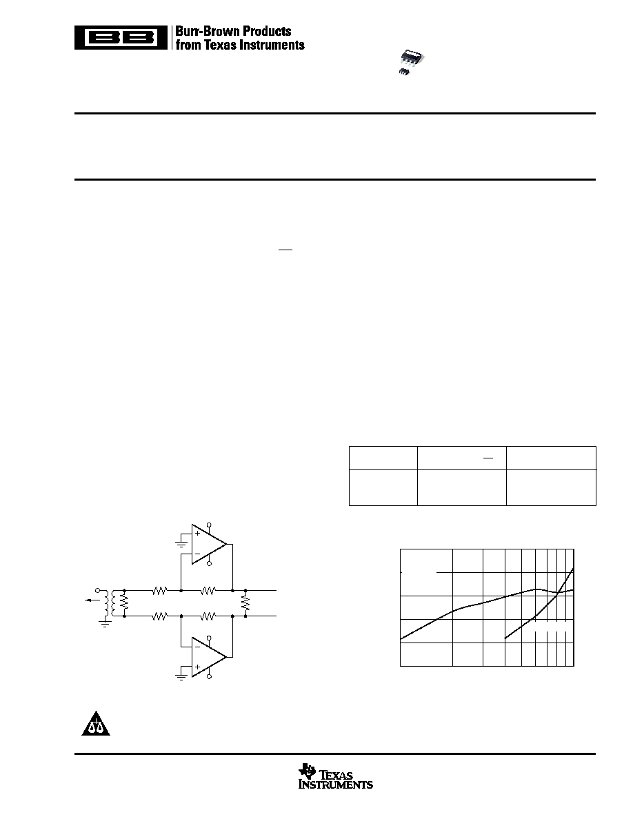
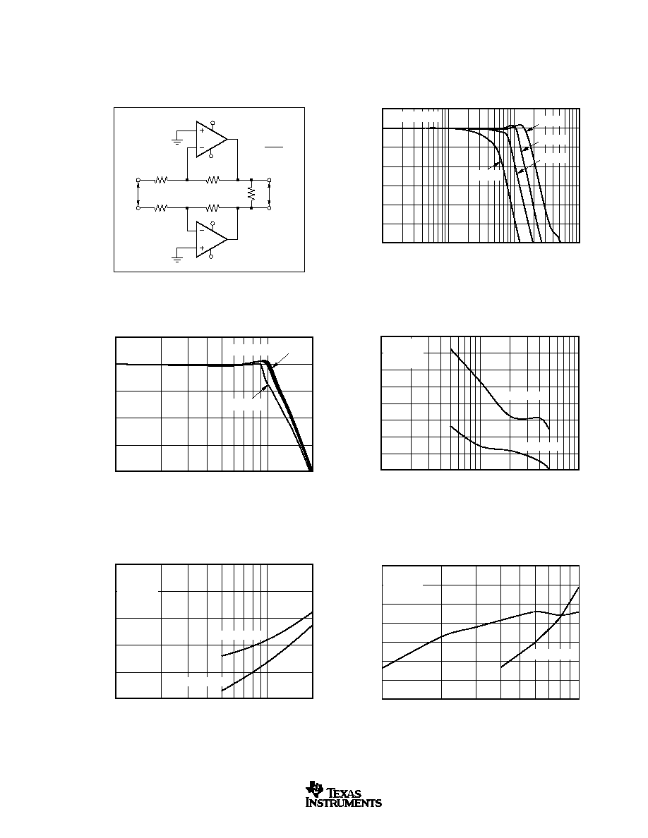
Differential configurations using two OPA843s can deliver
very low distortion to high output voltages, as shown below.
FEATURES
q
HIGH BANDWIDTH: 260MHz (G = +5)
q
GAIN BANDWIDTH PRODUCT: 800MHz
q
LOW INPUT VOLTAGE NOISE: 2.0nV/
Hz
q
VERY LOW DISTORTION: 96dBc (5MHz)
q
HIGH OPEN-LOOP GAIN: 110dB
q
FAST 12-BIT SETTLING: 10.5ns (0.01%)
q
LOW INPUT OFFSET VOLTAGE: 300
µ
V
q
OUTPUT CURRENT:
±
100mA
APPLICATIONS
q
ADC/DAC BUFFER AMPLIFIER
q
LOW DISTORTION "IF" AMPLIFIER
q
ACTIVE FILTERS
q
LOW-NOISE RECEIVER
q
WIDEBAND TRANSIMPEDANCE
q
TEST INSTRUMENTATION
q
PROFESSIONAL AUDIO
q
OPA643 UPGRADE
OPA843
SBOS268A DECEMBER 2002 OCTOBER 2003
www.ti.com
PRODUCTION DATA information is current as of publication date.
Products conform to specifications per the terms of Texas Instruments
standard warranty. Production processing does not necessarily include
testing of all parameters.
Copyright © 2002-2003, Texas Instruments Incorporated
Please be aware that an important notice concerning availability, standard warranty, and use in critical applications of
Texas Instruments semiconductor products and disclaimers thereto appears at the end of this data sheet.
All trademarks are the property of their respective owners.
Wideband, Low Distortion, Medium Gain,
Voltage-Feedback OPERATIONAL AMPLIFIER
INPUT NOISE
GAIN-BANDWIDTH
SINGLES
VOLTAGE (nV/
Hz )
PRODUCT (MHz)
OPA842
2.6
200
OPA846
1.2
1750
OPA847
0.85
3900
OPA843 RELATED PRODUCTS
OPA8
43
V
O
= 10V
I
V
I
1:1
50
132
OPA843
OPA843
+5V
+5V
5V
5V
Very Low Distortion Differential Driver
R
L
400
402
40.2
40.2
402
DIFFERENTIAL DISTORTION vs OUTPUT VOLTAGE
Output Voltage Swing (Vp-p)
Harmonic Distortion (dBc)
10
1
85
90
95
100
105
110
G
D
= 10
R
L
= 400
F = 5MHz
2nd-Harmonic
3rd-Harmonic
OPA843
2
SBOS268A
www.ti.com
SPECIFIED
PACKAGE
TEMPERATURE
PACKAGE
ORDERING
TRANSPORT
PRODUCT
PACKAGE-LEAD
DESIGNATOR
(1)
RANGE
MARKING
NUMBER
MEDIA, QUANTITY
OPA843
SO-8
D
40
°
C to +85
°
C
OPA843
OPA843ID
Rails, 100
"
"
"
"
"
OPA843IDR
Tape and Reel, 2500
OPA843
SOT23-5
DBV
40
°
C to +85
°
C
OARI
OPA843IDBVT
Tape and Reel, 250
"
"
"
"
"
OPA843IDBVR
Tape and Reel, 3000
NOTE: (1) For the most current specifications and package information, refer to our web site at www.ti.com.
PACKAGE/ORDERING INFORMATION
ABSOLUTE MAXIMUM RATINGS
(1)
Power Supply ...............................................................................
±
6.5V
DC
Internal Power Dissipation ...................................... See Thermal Analysis
Differential Input Voltage ..................................................................
±
1.2V
Input Voltage Range ............................................................................
±
V
S
Storage Voltage Range: D, DBV ................................... 40
°
C to +125
°
C
Lead Temperature (soldering, 10s) ............................................... +300
°
C
Junction Temperature (T
J
) ............................................................ +150
°
C
ESD Rating (Human Body Model) .................................................. 2000V
(Charge Device Model) ............................................... 1500V
(Machine Model) ........................................................... 200V
ELECTROSTATIC
DISCHARGE SENSITIVITY
This integrated circuit can be damaged by ESD. Texas Instru-
ments recommends that all integrated circuits be handled with
appropriate precautions. Failure to observe proper handling
and installation procedures can cause damage.
ESD damage can range from subtle performance degrada-
tion to complete device failure. Precision integrated circuits
may be more susceptible to damage because very small
parametric changes could cause the device not to meet its
published specifications.
NOTE: (1) Stresses above these ratings may cause permanent damage.
Exposure to absolute maximum conditions for extended periods may degrade
device reliability. These are stress ratings only, and functional operation of the
device at these or any other conditions beyond those specified is not implied.
PIN CONFIGURATIONS
Top View
SO
Top View
SOT
1
2
3
4
8
7
6
5
NC
+V
S
Output
NC
NC = No Connection
NC
Inverting Input
Noninverting Input
V
S
1
2
3
5
4
+V
S
Inverting Input
Output
V
S
Noninverting Input
OARI
1
2
3
5
4
Pin Orientation/Package Marking
OPA843
3
SBOS268A
www.ti.com
AC PERFORMANCE (see Figure 1)
Small-Signal Bandwidth (V
O
= 200mVp-p)
G = +3
500
MHz
typ
C
G = +5
260
185
180
175
MHz
min
B
G = +10
85
66
65
64
MHz
min
B
G = +20
40
30
30
30
MHz
min
B
Gain-Bandwidth Product
800
562
560
558
MHz
min
B
Bandwidth for 0.1dB Gain Flatness
G = +5, R
L
= 100
, V
O
= 200mVp-p
65
34
33
32
MHz
min
B
Peaking at a Gain of +3
3.5
dB
typ
C
Harmonic Distortion
G = +5, f = 5MHz, V
O
= 2Vp-p
2nd-Harmonic
R
L
= 100
76
74
72
70
dBc
max
B
R
L
= 500
96
94
92
90
dBc
max
B
3rd-Harmonic
R
L
= 100
102
100
98
95
dBc
max
B
R
L
=
500
110
105
102
100
dBc
max
B
2-Tone, 3rd-Order Intercept
G = +5, f = 25MHz
40
dBm
typ
C
Input Voltage Noise
f > 1MHz
2.0
2.2
2.31
2.36
nV/
Hz
max
B
Input Current Noise
f > 1MHz
2.8
3.35
3.4
3.45
pA/
Hz
max
B
Rise-and-Fall Time
0.2V Step
1.2
1.95
2.0
2.1
ns
max
B
Slew Rate
2V Step
1000
650
600
525
V/
µ
s
min
B
Settling Time to 0.01%
2V Step
10.5
ns
typ
C
0.1%
2V Step
7.5
10
10.3
10.6
ns
max
B
1.0%
2V Step
3.2
5.4
5.8
6.4
ns
max
B
Differential Gain
G = +4, NTSC, R
L
= 150
0.001
%
typ
C
Differential Phase
G = +4, NTSC, R
L
= 150
0.012
deg
typ
C
DC PERFORMANCE
(4)
Open-Loop Voltage Gain (A
OL
)
V
O
= 0V
110
100
96
92
dB
min
A
Input Offset Voltage
V
CM
= 0V
±
0.30
±
1.20
±
1.4
±
1.5
mV
max
A
Average Offset Voltage Drift
V
CM
= 0V
±
4
±
4
µ
V/
°
C
max
B
Input Bias Current
V
CM
= 0V
20
35
36
37
µ
A
max
A
Input Bias Current Drift
V
CM
= 0V
25
25
nA/
°
C
max
B
Input Offset Current
V
CM
= 0V
±
0.25
±
1.0
±
1.15
±
1.17
µ
A
max
A
Input Offset Current Drift
V
CM
= 0V
±
2
±
2
nA/
°
C
max
B
INPUT
Common-Mode Input Range (CMIR)
(5)
±
3.2
±
3.0
±
2.9
±
2.8
V
min
A
Common-Mode Rejection (CMRR)
V
CM
=
±
1V, Input Referred
95
85
84
82
dB
min
A
Input Impedance
Differential-Mode
V
CM
= 0V
12 || 1
k
|| pF
typ
C
Common-Mode
V
CM
= 0V
3.2 || 1.2
M
|| pF
typ
C
OUTPUT
Output Voltage Swing
R
L
> 1k
, Positive Output
3.2
3.0
2.9
2.8
V
min
A
R
L
> 1k
, Negative Output
3.7
3.5
3.4
3.3
V
min
A
R
L
= 100
, Positive Output
3.0
2.8
2.7
2.6
V
min
A
R
L
= 100
, Negative Output
3.5
3.3
3.2
3.1
V
min
A
Current Output
V
O
= 0V
±
100
±
90
±
85
±
80
mA
min
A
Closed-Loop Output Impedance
G = +5, f = 1kHz
0.0001
typ
C
POWER SUPPLY
Specified Operating Voltage
±
5
V
typ
C
Maximum Operating Voltage
±
6
±
6
±
6
V
max
A
Minimum Operating Voltage
±
4
±
4
±
4
V
min
A
Max Quiescent Current
V
S
=
±
5V
20.2
20.8
22.2
22.5
mA
max
A
Min Quiescent Current
V
S
=
±
5V
20.2
19.6
19.1
18.3
mA
min
A
Power-Supply Rejection Ratio
(+PSRR, PSRR)
|V
S
| = 4.5V to 5.5V, Input Referred
100
90
88
85
dB
min
A
THERMAL CHARACTERISTICS
Specified Operating Range: D, DBV
40 to +85
°
C
typ
C
Thermal Resistance,
JA
Junction-to-Ambient
D
SO-8
125
°
C
typ
C
DBV
SOT23-5
150
°
C
typ
C
OPA843ID, OPA843IDBV
TYP
MIN/MAX OVER TEMPERATURE
0
°
C to
40
°
C to
MIN/
TEST
PARAMETER
CONDITIONS
+25
°
C
+25
°
C
(1)
70
°
C
+85
°
C
(2)
UNITS
MAX
LEVEL
(3 )
ELECTRICAL CHARACTERISTICS: V
S
=
±
5V
Boldface limits are tested at +25
°
C.
At T
A
= +25
°
C, V
S
=
±
5V, R
F
= 402
, R
L
= 100
, and G = +5, unless otherwise noted. See Figure 1 for AC performance.
NOTES: (1) Junction temperature = ambient temperature for 25
°
C min/max specifications. (2) Junction temperature = ambient at low temperature limit: junction
temperature = ambient +23
°
C at high temperature limit for over temperature min/max specifications. (3) Test Levels: (A) 100% tested at 25
°
C over-temperature
limits by characterization and simulation. (B) Limits set by characterization and simulation. (C) Typical value only for information. (4) Current is considered positive out-
of-node. V
CM
is the input common-mode voltage. (5) Tested < 3dB below minimum specified CMRR at
±
CMIR limits.
OPA843
4
SBOS268A
www.ti.com
TYPICAL CHARACTERISTICS: V
S
=
±
5V
T
A
= +25
°
C, G = +5, R
F
= 402
, R
G
= 100
, and R
L
= 100
, unless otherwise noted.
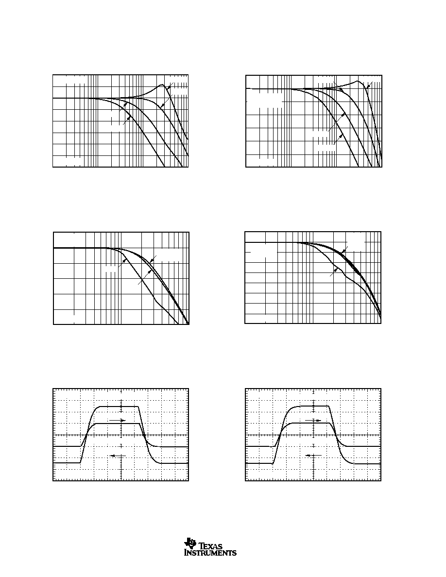
NONINVERTING SMALL-SIGNAL
FREQUENCY RESPONSE
Frequency (Hz)
10
6
10
8
10
7
10
9
Normalized Gain (dB)
6
3
0
3
6
9
12
15
18
V
O
= 0.2Vp-p
G = +5
G = +3
G = +10
G = +20
See Figure 1
INVERTING SMALL-SIGNAL
FREQUENCY RESPONSE
Frequency (Hz)
10
6
10
8
10
7
10
9
Normalized Gain (dB)
3
0
3
6
9
12
15
18
R
G
= R
S
= 50
V
O
= 0.2Vp-p
G = 8
G = 4
G = 16
G = 32
See Figure 2
NONINVERTING LARGE-SIGNAL
FREQUENCY RESPONSE
Frequency (Hz)
10
7
10
8
10
9
Gain (dB)
17
14
11
8
5
2
1
R
L
= 100
G = +5V/V
2Vp-p
200mVp-p
to 1Vp-p
5Vp-p
See Figure 1
INVERTING LARGE-SIGNAL
FREQUENCY RESPONSE
Frequency (Hz)
10
7
10
8
10
9
Gain (dB)
21
18
15
12
9
6
3
0
3
6
R
L
= 100
G = 8V/V
0.2Vp-p
1Vp-p
2Vp-p
5Vp-p
See Figure 2
NONINVERTING PULSE RESPONSE
Time (2ns/div)
Output Voltage (100mV/div)
Output Voltage (400mV/div)
200
100
0
100
200
1.2
0.8
0.4
0
0.4
0.8
1.2
G = +5
See Figure 1
Large Signal
±
1V
Small Signal
±
100mV
Right Scale
Left Scale
INVERTING PULSE RESPONSE
Time (2ns/div)
Output Voltage (100mV/div)
Output Voltage (400mV/div)
200
100
0
100
200
1.2
0.8
0.4
0
0.4
0.8
1.2
Large Signal
±
1V
See Figure 2
Small Signal
±
100mV
Right Scale
Left Scale
G = 8
OPA843
5
SBOS268A
www.ti.com
TYPICAL CHARACTERISTICS: V
S
=
±
5V
(Cont.)
T
A
= +25
°
C, G = +5, R
F
= 402
, R
G
= 100
, and R
L
= 100
, unless otherwise noted.
5MHz HARMONIC DISTORTION vs LOAD RESISTANCE
Resistance (
)
100
150
200
250
300
350
400
450
500
Harmonic Distortion (dBc)
75
80
85
90
95
100
105
110
V
O
= 2Vp-p
G = +5
2nd-Harmonic
3rd-Harmonic
See Figure 1
1MHz HARMONIC DISTORTION vs LOAD RESISTANCE
Resistance (
)
100
150
200
250
300
350
400
450
500
Harmonic Distortion (dBc)
75
80
85
90
95
100
105
110
V
O
= 5Vp-p
G = +5
3rd-Harmonic
2nd-Harmonic
See Figure 1
HARMONIC DISTORTION vs FREQUENCY
Frequency (MHz)
0.1
10
1
100
Harmonic Distortion (dBc)
60
70
80
90
100
110
V
O
= 2Vp-p
G = +5
R
L
= 200
2nd-Harmonic
3rd-Harmonic
See Figure 1
HARMONIC DISTORTION vs OUTPUT VOLTAGE
Output Voltage Swing (Vp-p)
0.1
1
10
Harmonic Distortion (dBc)
70
75
80
85
90
95
100
105
110
R
L
= 200
F = 5MHz
G = +5
2nd-Harmonic
3rd-Harmonic
See Figure 1
HARMONIC DISTORTION vs NONINVERTING GAIN
Gain (V/V)
5
10
15
20
Harmonic Distortion (dBc)
70
80
90
100
110
V
O
= 2Vp-p
R
L
= 200
F = 5MHz
R
F
= 402
, R
G
Adjusted
2nd-Harmonic
3rd-Harmonic
See Figure 1
HARMONIC DISTORTION vs INVERTING GAIN
Gain
(V/V)
5
10
15
20
25
30
35
40
Harmonic Distortion (dBc)
75
85
95
105
115
2nd-Harmonic
3rd-Harmonic
V
O
= 2Vp-p
R
L
= 200
F = 5MHz
R
G
= 50
, R
F
Adjusted
See Figure 2
OPA843
6
SBOS268A
www.ti.com
TYPICAL CHARACTERISTICS: V
S
=
±
5V
(Cont.)
T
A
= +25
°
C, G = +5, R
F
= 402
, R
G
= 100
, and R
L
= 100
, unless otherwise noted.
INPUT VOLTAGE AND CURRENT NOISE DENSITY
Frequency (Hz)
10
2
10
4
10
5
10
6
10
3
10
7
Voltage Noise nV/
Hz
Current Noise pA/
Hz
10
1
Voltage Noise
Current Noise
2.0nV/
Hz
2.8pA/
Hz
2-TONE, 3RD-ORDER
INTERMODULATION INTERCEPT
Frequency (MHz)
10
15
20
25
30
35
40
45
50
55
60
65
70
Intercept Point (+dBm)
55
50
45
40
35
30
25
G = +5
OPA843
50
50
50
402
100
P
O
P
I
NONINVERTING GAIN FLATNESS TUNE
Frequency (MHz)
1
100
10
1k
Deviation from 12dB Gain (0.1dB/div)
0.40
0.30
0.20
0.10
0
0.10
0.20
0.30
0.40
V
O
= 200mVp-p
A
V
= +4
NG = 4.5
NG = 4
NG = 5.5
NG = 5
External Compensation
See Figure 10
LOW GAIN INVERTING BANDWIDTH
Frequency (MHz)
1
100
10
1k
Normalized Gain (1dB/div)
3
2
1
0
1
2
3
4
5
6
V
O
= 200mVp-p
G = 2
G = 1
G = 3
External Compensation
See Figure 11
RECOMMENDED R
S
vs CAPACITIVE LOAD
Capacitive Load (pF)
1
10
100
1k
R
S
(
)
100
10
1
G = +5
FREQUENCY RESPONSE vs CAPACITIVE LOAD
Frequency (Hz)
10
6
10
8
10
7
10
9
Normalized Gain to Capacitive Load (dB)
17
14
11
8
5
2
R
S
adjusted to cap load.
C = 10pF
C = 22pF
OPA843
R
S
50
1k
C
L
402
100
V
O
V
I
1k
is optional.
C = 100pF
C = 47pF
OPA843
7
SBOS268A
www.ti.com
TYPICAL CHARACTERISTICS: V
S
=
±
5V
(Cont.)
T
A
= +25
°
C, G = +5, R
F
= 402
, R
G
= 100
, and R
L
= 100
, unless otherwise noted.
CMRR AND PSRR vs FREQUENCY
Frequency (Hz)
10
1
10
4
10
3
10
2
10
5
10
6
10
7
10
8
Common-Mode Rejection Ratio (dB)
Power-Supply Rejection Ratio (dB)
120
100
80
60
40
20
0
CMRR
+PSRR
PSRR
OPEN-LOOP GAIN AND PHASE
Frequency (Hz)
10
1
10
3
10
2
10
4
10
5
10
6
10
7
10
8
10
9
Open-Loop Gain (dB)
120
100
80
60
40
20
0
20
Open-Loop Phase (
°
)
0
30
60
90
120
150
180
210
A
OL
20log (A
OL
)
OUTPUT VOLTAGE AND CURRENT LIMITATIONS
I
O
(mA)
0.15
0.1
0.05
0
0.05
0.1
0.15
V
O
(V)
4
3
2
1
0
1
2
3
4
1W Internal
Power Limit
1W Internal
Power Limit
R
L
= 25
R
L
= 100
R
L
= 50
CLOSED-LOOP OUTPUT IMPEDANCE
vs FREQUENCY
Frequency (Hz)
10
2
10
3
10
4
10
5
10
6
10
7
10
8
Output Impedance (
)
10
1
0.1
0.01
0.001
0.0001
0.00001
OPA843
402
100
Z
O
NONINVERTING OVERDRIVE RECOVERY
Time (40ns/div)
Output Voltage (1V/div)
Input Voltage (200mV/div)
5
4
3
2
1
0
1
2
3
4
5
1
0.8
0.6
0.4
0.2
0
0.2
0.4
0.6
0.8
1
Output
Left Scale
Input
Right Scale
R
L
= 100
G = 5
See Figure 1
INVERTING OVERDRIVE RECOVERY
Time (40ns/div)
Output Voltage (1V/div)
Input Voltage (200mV/div)
5
4
3
2
1
0
1
2
3
4
5
1
0.8
0.6
0.4
0.2
0
0.2
0.4
0.6
0.8
1
Output
Left Scale
Input
Right Scale
R
L
= 100
G = 8
See Figure 2
OPA843
8
SBOS268A
www.ti.com
TYPICAL CHARACTERISTICS: V
S
=
±
5V
(Cont.)
T
A
= +25
°
C, G = +5, R
F
= 402
, R
G
= 100
, and R
L
= 100
, unless otherwise noted.
SETTLING TIME
Time (ns)
0
5
10
15
20
25
Percent of Final Value (%)
0.25
0.20
0.15
0.10
0.05
0
0.05
0.10
0.15
0.20
0.25
R
L
= 100
V
O
= 2V step
G = +5
See Figure 1
VIDEO DIFFERENTIAL GAIN/DIFFERENTIAL PHASE
Video Loads (150
each)
1
2
3
4
5
Differential Gain (%)
Differential Phase (
°
)
0.02
0.015
0.01
0.005
0
0.1
0.075
0.05
0.025
0
G = +4
dP, Negative Video
dG, Positive Video
dP, Positive Video
dG, Negative Video
TYPICAL DC DRIFT OVER TEMPERATURE
Ambient Temperature (
°
C)
50
25
0
25
50
75
100
125
Input Offset Voltage (mV)
Input Bias and Offset Current (
µ
A)
1
0.5
0
0.5
1
25
12.5
0
12.5
25
V
IO
I
B
100 x I
OS
SUPPLY AND OUTPUT CURRENT vs TEMPERATURE
Ambient Temperature (
°
C)
50
25
0
25
50
75
100
125
Output Current (2mA/div)
Supply Current (1mA/div)
110
106
102
98
94
90
22
21
20
19
18
17
Supply Current
Sourcing Output Current
Sinking Output Current
COMMON-MODE INPUT RANGE AND OUTPUT SWING
vs SUPPLY VOLTAGE
Supply Voltage (
±
V)
3
4
5
6
Voltage Range (V)
6
4
2
0
2
4
6
Positive Output
Negative Input
Negative Output
Positive Input
COMMON-MODE AND DIFFERENTIAL
INPUT IMPEDANCE
Frequency (Hz)
10
3
10
4
10
5
10
6
10
7
10
8
Impedance Magnitude (20log (
))
10
7
10
6
10
5
10
4
10
3
10
2
Common-Mode
Differential
OPA843
9
SBOS268A
www.ti.com
TYPICAL CHARACTERISTICS: V
S
=
±
5V
(Cont.)
T
A
= +25
°
C, G
D
= 10, R
F
= 1k
, R
G
= 100
, and R
L
= 100
, unless otherwise noted.
OPA843
OPA843
R
G
100
R
F
+5V
R
G
100
R
L
V
I
R
F
V
O
5V
+5V
5V
G
D =
R
F
100
DIFFERENTIAL SMALL-SIGNAL
FREQUENCY RESPONSE
Frequency (MHz)
1
100
10
1k
Normalized Gain (dB)
3
0
3
6
9
12
15
18
V
O
= 400mVp-p
G
D
= 5
G
D
= 16
G
D
= 10
G
D
= 32
DIFFERENTIAL LARGE-SIGNAL
FREQUENCY RESPONSE
Frequency (MHz)
10
100
200
Gain (dB)
23
20
17
14
11
8
G
D
= 10V/V
V
O
= 400mVp-p to 5Vp-p
V
O
= 8Vp-p
DIFFERENTIAL DISTORTION vs LOAD RESISTANCE
Load Resistance (
)
10
100
1k
Harmonic Distortion (dBc)
70
75
80
85
90
95
100
105
110
V
O
= 4Vp-p
G
D
= 10
F = 5MHz
2nd-Harmonic
3rd-Harmonic
DIFFERENTIAL DISTORTION vs FREQUENCY
Frequency (Hz)
1
10
20
Gain (dB)
60
70
80
90
100
110
V
O
= 4Vp-p
G
D
= 10
R
L
= 400
2nd-Harmonic
3rd-Harmonic
DIFFERENTIAL DISTORTION vs OUTPUT VOLTAGE
Output Voltage Swing (Vp-p)
Harmonic Distortion (dBc)
10
1
80
85
90
95
100
105
110
115
G
D
= 10
R
L
= 400
F = 5MHz
2nd-Harmonic
3rd-Harmonic
DIFFERENTIAL PERFORMANCE
TEST CIRCUIT
OPA843
10
SBOS268A
www.ti.com
FIGURE 1. Gain of +5, High-Frequency Application and
Characterization Circuit.
APPLICATIONS INFORMATION
WIDEBAND NONINVERTING OPERATION
The OPA843's combination of speed and dynamic range is
useful in a wide variety of application circuits, as long as
simple guidelines common to all high-speed amplifiers are
observed. For example, good power-supply decoupling, as
shown in Figure 1, is essential to achieve the lowest possible
harmonic distortion and smooth frequency response. Careful
PC board layout and component selection will maximize the
performance of the OPA843 in all applications, as discussed
in the following sections of this data sheet. Figure 1 shows
the gain of +5 configuration used as the basis for most of the
typical characteristics. Most of the curves were characterized
using signal sources with 50
driving impedance and with
measurement equipment presenting 50
load impedance. In
Figure 1, the 50
shunt resistor at the input terminal matches
the source impedance of the test generator, while the 50
series resistor at the V
O
terminal provides a matching resistor
for the measurement equipment load. Generally, data sheet
specifications refer to the voltage swing at the output pin (V
O
in Figure 1) while those referring to load power are at the 50
load. The total 100
load from the series and shunt matching
resistors, combined with the 502
total feedback network
load, presents the OPA843 with an effective output load of
approximately 83
.
both the input termination resistor and the gain setting
resistor for the circuit. Although the signal gain for the circuit
of Figure 2 is equal to 8V/V (versus the +5V/V for Figure 1),
their noise gains are equal when the 50
source resistor is
included. This has the interesting effect of nearly doubling
the equivalent Gain Bandwidth Product (GBP) for the ampli-
fier. This can be seen in comparing the G = +5 and G = 8
small-signal frequency response curves. Both show approxi-
mately 260MHz bandwidth, but the inverting configuration of
Figure 2 is giving 4dB higher signal gain. If the signal source
is actually the low impedance output of another amplifier, R
G
is increased to the minimum value allowed at the output of
that amplifier and R
F
is adjusted to get the desired gain. It is
critical for stable operation of the OPA843 that this driving
amplifier show a very low output impedance through frequen-
cies exceeding the expected closed-loop bandwidth for the
OPA843.
An optional input termination resistor is also shown in Figure 2.
This R
M
resistor may be used to adjust the input impedance to
lower values when R
G
needs to be adjusted higher. This might
be desirable at lower gains where increasing R
F
will reduce the
output loading improving harmonic distortion performance. For
instance, at a gain of 4 an R
G
set to 50
will require a 200
feedback resistor. In this case, adjusting R
F
to 400
, setting R
G
to 100
, and then adding a 100
R
M
resistor will deliver a gain
of 4 with a 50
input match.
BUFFERING HIGH-PERFORMANCE ADCs
A single-channel interface using the OPA843 can provide a low
noise/distortion interface to emerging 14-bit Analog-to-Digital
Converters (ADCs) through approximately 5MHz for medium
gain applications. Since the dominant distortion mechanism is
2nd-harmonic distortion, differential circuits using the OPA843
can extend this frequency range and/or power level to much
higher levels. The example on the front page of this data sheet,
for instance, shows better than 93dB SFDR at 5MHz for up to
8Vp-p signals. This is still being limited by the 2nd-harmonic with
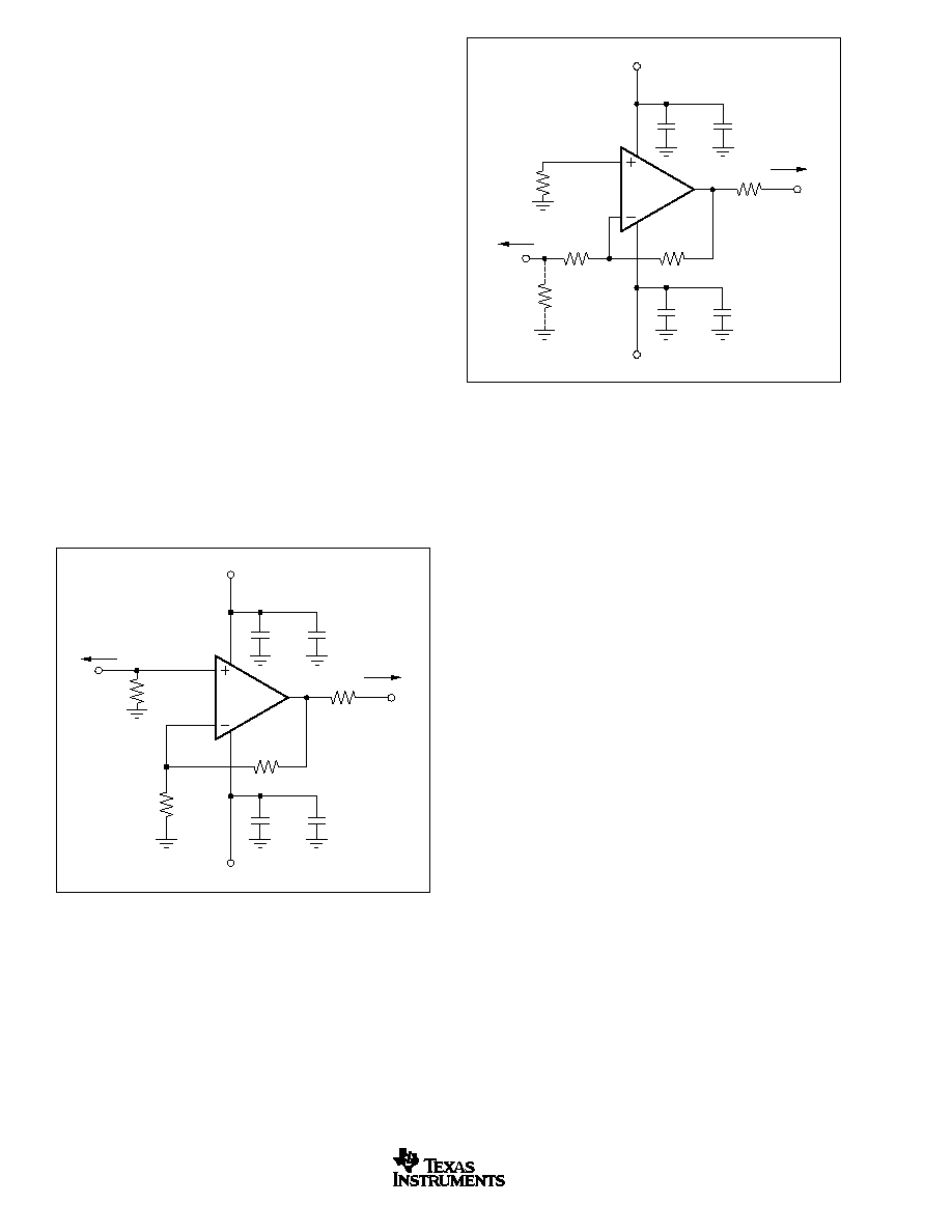
WIDEBAND, INVERTING GAIN OPERATION
There can be significant benefits to operating the OPA843 as
an inverting amplifier. This is particularly true when a matched
input impedance is required. Figure 2 shows the inverting
gain circuit used as a starting point for the typical character-
istics showing inverting mode performance.
Driving this circuit from a 50
source, and constraining the
gain resistor, R
G
, to equal 50
will give both a signal
bandwidth and noise advantage. R
G
in this case is acting as
OPA843
+5V
5V
V
S
+V
S
R
S
50
V
O
V
IN
50
+
2.2
µ
F
+
2.2
µ
F
0.1
µ
F
R
G
100
R
F
402
50
Source
50
Load
0.1
µ
F
FIGURE 2. Inverting G = 8 Specification and Test Circuit.
OPA843
+5V
5V
R
S
50
V
O
V
I
R
T
+
2.2
µ
F
+
2.2
µ
F
0.1
µ
F
R
M
(optional)
R
F
402
50
Source
50
Load
0.1
µ
F
R
G
50
OPA843
11
SBOS268A
www.ti.com
the 3rd-harmonic much lower. 2-tone 3rd-order intermodulation
terms will be much lower than most other solutions using the
circuit shown on the front page. The differential typical charac-
teristic curves also show that a 4Vp-p output will have
> 80dBc SFDR through 20MHz using this differential approach.
WIDE DYNAMIC RANGE "IF" AMPLIFIER
The OPA843 offers an attractive alternative to standard fixed-
gain IF amplifier stages. Narrowband systems will benefit from
the exceptionally high 2-tone 3rd-order intermodulation inter-
cept, as shown in the Typical Characteristics. Op amps with
high open-loop gain, like the OPA843, provide an intercept
that decreases with frequency along with the loop gain. The
OPA843's 3rd-order intercept shows a decreasing intercept
with frequency. The OPA843's intercept is > 30dBm up to
50MHz but improves to > 50dBm as the operating frequency
is reduced below 10MHz. Broadband systems will also benefit
from the very low even-order harmonics and intermodulation
components produced by the OPA843. Compared to standard
fixed-gain IF amplifiers, the OPA843 operating at IF's below
50MHz provides much higher intercepts for its quiescent
power dissipation (200mW), superior gain accuracy, higher
reverse isolation, and lower I/O return loss. The noise figure
for the OPA843 will be higher than alternative fixed-gain
stages. If the application comes late in the amplifier chain with
significant gain in prior stages, this higher noise figure may be
acceptable. Figure 3 shows an example of a noninverting
configuration for the OPA843 used as an IF amplifier.
1dB through 50MHz. For narrowband IF's in the 44MHz
region, this configuration of the OPA843 will show a 3rd-order
intercept of 33dBm while dissipating only 200mW (23dBm)
power from
±
5V supplies.
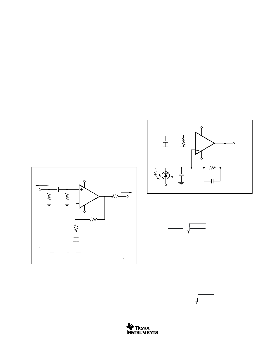
PHOTODIODE TRANSIMPEDANCE AMPLIFIER
High Gain Bandwidth Product (GBP) and low input voltage
and current noise make the OPA843 an ideal wideband
transimpedance amplifier for low to moderate gains. Note
that unity-gain stability is not required for transimpedance
applications. Figure 4 shows an example photodiode ampli-
fier circuit. The key parameters of this design are the esti-
mated diode capacitance (C
D
) at the applied DC reverse bias
voltage (V
B
), the desired transimpedance gain (R
F
), and the
GBP for the OPA843 (800MHz). With these three variables
set (and adding the OPA843's parasitic input capacitance to
the value of C
D
to get C
S
), the feedback capacitor value (C
F
)
is selected to provide stability for the transimpedance fre-
quency response.
The input signal and the gain resistor are AC coupled through
the 0.01
µ
F blocking capacitors. This holds the DC input and
output operating point at ground independent of source im-
pedance and gain setting. The R
G
value in Figure 3 (144
),
sets the gain to the matched load at 12dB. Using standard 1%
tolerance resistors for R
F
and R
G
will hold the gain to a
±
0.2dB
tolerance. This example will give a 3dB bandwidth of ap-
proximately 100MHz while maintaining gain flatness within
To achieve a maximally flat 2nd-order Butterworth frequency
response, the feedback pole should be set to:
1
2
4
R C
GBP
R C
F
F
F
S
C
C
C
S
D
I
=
=
+
(1)
Adding the OPA843's common-mode and differential mode
input capacitances C
I
= (1.0 + 1.2)pF to the 20pF diode
source capacitance of Figure 4, and targeting a 10k
tran-
simpedance gain using the 800MHz GBP for the OPA843,
the required feedback pole frequency is 16.9MHz. This will
require a total feedback capacitance of 0.94pF. Typical
surface-mount resistors have a parasitic capacitance of
0.2pF, leaving the required 0.75pF value shown in Figure 4
to get the required feedback pole.
This will set the 3dB bandwidth according to:
F
GBP
R C
Hz
dB
F
S
-
3
2
(2)
The example of Figure 4 will give approximately 24MHz
3dB bandwidth using the 0.75pF feedback compensation.
OPA843
+5V
+5V
R
S
50
V
O
P
I
P
0
0.01
µ
F
R
G
144
1k
52.3
R
F
1k
50
Source
50
Load
0.01
µ
F
Power-supply
decoupling not shown.
Gain
=
P
I
P
O
=
20log
1
2
1
+
R
F
R
G
dB
=
12dB with values shown
FIGURE 3. High Dynamic Range IF Amplifier.
R
F
10k
Power-supply decoupling
not shown.
OPA843
+5V
5V
V
B
C
F
0.75pF
I
D
V
O
= I
D
R
F
C
D
20pF
0.01
µ
F
10k
FIGURE 3. High Dynamic Range IF Amplifier.
OPA843
12
SBOS268A
www.ti.com
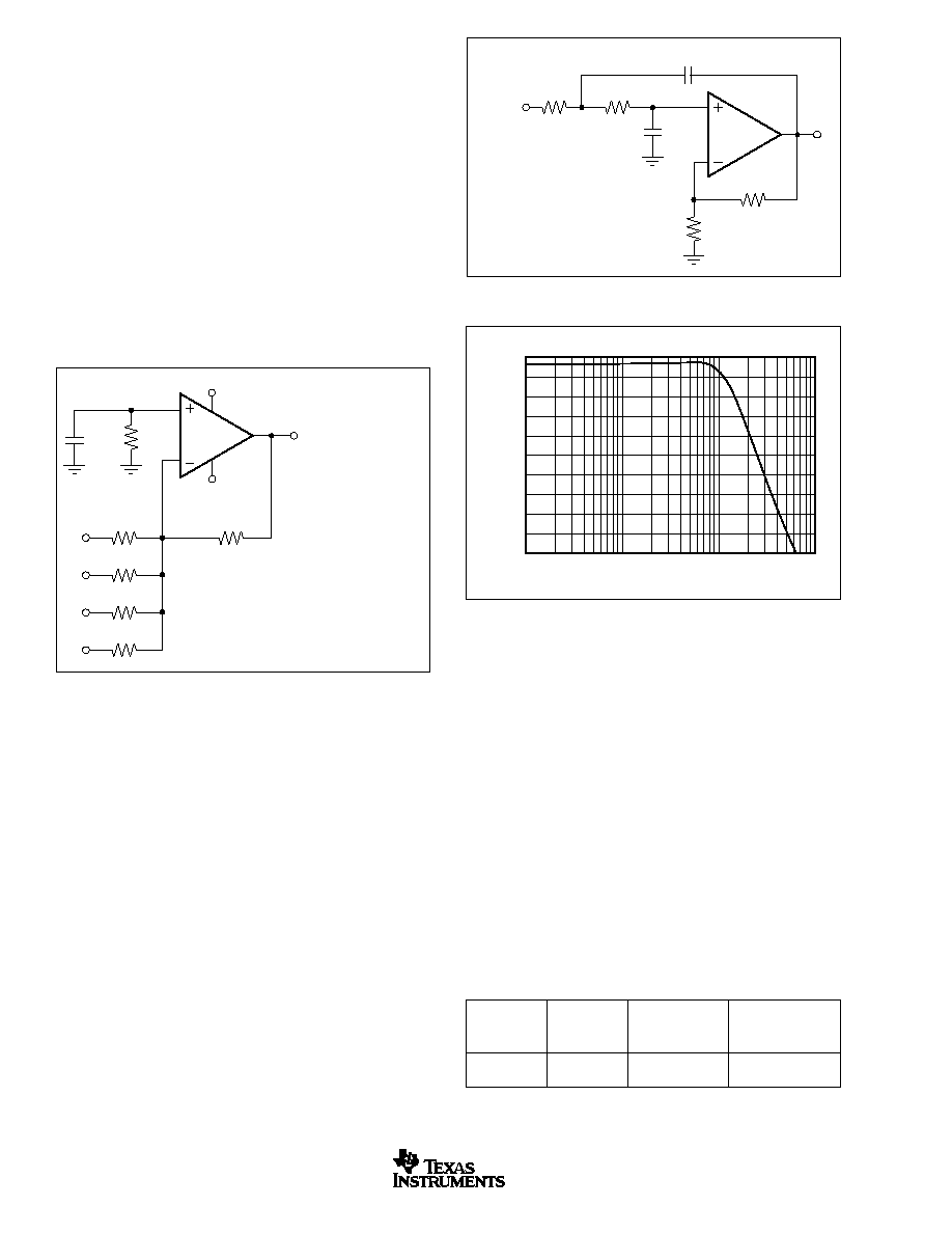
WIDEBAND INVERTING SUMMING AMPLIFIER
One common application for a wideband op amp like the
OPA843 is to sum a number of signal sources together.
Figure 5 shows the inverting summing configuration that is
most often used. This circuit offers the benefit that each input
sees an input impedance set only by its individual input
resistor, since the summing junction (inverting op amp node)
is a virtual ground. Each input is non-interactive with every
other. However, the bandwidth from any input to the summed
output is set by the op amp noise gain (NG), which is equal
to the noninverting voltage gain. Therefore, each inverting
channel may have a low gain to the output (like the 1 shown
in Figure 5); this noise gain will set the frequency response
and the loop stability. The noninverting gain for Figure 5 is
equal to +5, which will give a 260MHz bandwidth at a gain of
1 for each of the input signals.
transition from a unity gain receiver at lower frequencies
(through the R
5
path) to a gain of 20dB (10V/V) through the
R
1
path at higher frequencies. The component values have
been selected to set the peak gain at approximately 30MHz.
A unique feature for this circuit is an independent tune on the
width of the peaking (Q of the response) by adjusting R
G
.
See Figure 9 for the effect of adjusting R
G
over the range of
20
to 100
.
DESIGN-IN TOOLS
DEMONSTRATION BOARDS
Two PC boards are available to assist in the initial evaluation
of circuit performance using the OPA843 in its two package
styles. Both of these are available, free, as an unpopulated PC
board delivered with descriptive documentation. The summary
information for these boards is shown in the table below.
2nd-Order Filter Topology
High-speed amplifiers like the OPA843 are good choices for
2nd-order filter building blocks as part of ADC driver chan-
nels. These can provide noise bandlimiting to improve the
SNR for the amplifier/converter combination. The circuit of
Figure 6 shows an example of a 10MHz Butterworth low-
pass filter where the amplifier provides a low frequency gain
of 5 and a 2nd-order cutoff at 10MHz. The resistor values
have been adjusted slightly to account for the amplifier
bandwidth. Figure 7 shows the small-signal frequency re-
sponse for this filter.
EQUALIZING FILTER APPLICATION
In sensor receiver applications, where the pickup is a sensor
or cable giving a bandlimited frequency response, an equal-
izing filter can sometimes be used to extend the useable
frequency range for the sensor. This is done mathematically
by taking the inverse of the rolloff transfer function and
implementing that as the amplifier frequency response. See
Figure 8 for one example of a wideband equalizer where two
stages of the OPA843 are used. This example is set to
Contact your sales representative or go to the TI web site
(www.ti.com) to request evaluation boards.
R
F
402
OPA843
+5V
5V
0.1
µ
F
402
81.8
V
O
= (V
1
+ V
2
+ V
3
+ V
4
)
V
1
402
V
2
402
V
3
402
V
4
Power-supply decoupling not shown.
FIGURE 5. Wideband Inverting Summing Amplifier.
OPA843
150
100pF
61
0
Source
100
402
220pF
V
I
V
O
Frequency (MHz)
10MHz Low-Pass Filter
100k
1M
10M
100M
Gain (dB)
15
12
9
6
3
0
3
6
9
12
15
FIGURE 6. 10MHz Butterworth Low-Pass Filter.
FIGURE 7. Frequency Response for Figure 6.
LITERATURE
BOARD
REQUEST
PRODUCT
PACKAGE
PART NUMBER
NUMBER
OPA843U
SO-8
DEM-OPA68xU
SBOU010
OPA843N
SOT23-5
DEM-OPA6xx
SBOU009
OPA843
13
SBOS268A
www.ti.com
MACROMODELS AND APPLICATIONS SUPPORT
Computer simulation of circuit performance using SPICE is
often a quick way to analyze the performance of the OPA843
and its circuit designs. This is particularly true for video and
RF amplifier circuits where parasitic capacitance and induc-
tance can play a major role on circuit performance. A SPICE
model for the OPA843 is available through the TI web page
(http://www.ti.com). The applications department is also avail-
able for design assistance. These models predict typical
small-signal AC, transient steps, DC performance, and noise
under a wide variety of operating conditions. The models
include the noise terms found in the electrical specifications
of this data sheet. These models do not attempt to distin-
guish between the package types in their small-signal AC
performance.
OPERATING SUGGESTIONS
OPTIMIZING RESISTOR VALUES
Since the OPA843 is a voltage-feedback op amp, a wide
range of resistor values may be used for the feedback and
gain setting resistors. The primary limits on these values are
set by dynamic range (noise and distortion) and parasitic
capacitance considerations. Usually, the feedback resistor
value should be between 200
and 1k
. Below 200
, the
feedback network will present additional output loading that
can degrade the harmonic distortion performance of the
OPA843. Above 1k
, the typical parasitic capacitance (ap-
proximately 0.2pF) across the feedback resistor may cause
unintentional band limiting in the amplifier response.
A good rule of thumb is to target the parallel combination of
R
F
and R
G
(see Figure 1) to be less than about 200
. The
combined impedance R
F
|| R
G
interacts with the inverting
input capacitance, placing an additional pole in the feedback
network, and thus a zero in the forward response. Assuming
a 2pF total parasitic on the inverting node, holding R
F
|| R
G
< 200
will keep this pole above 400MHz. By itself, this
constraint implies that the feedback resistor R
F
can increase
to several k
at high gains. This is acceptable as long as the
pole formed by R
F
and any parasitic capacitance appearing
in parallel is kept out of the frequency range of interest.
In the inverting configuration, an additional design consider-
ation must be noted. R
G
becomes the input resistor and,
therefore, the load impedance to the driving source. If imped-
ance matching is desired, R
G
may be set equal to the
required termination value. However, at low inverting gains
the resultant feedback resistor value can present a signifi-
cant load to the amplifier output. For example, an inverting
gain of 4 with a 50
input matching resistor (= R
G
) would
require a 200
feedback resistor, which would contribute to
output loading in parallel with the external load. In such a
case, it would be preferable to increase both the R
F
and R
G
values, and then achieve the input matching impedance with
a third resistor to ground, see Figure 2. The total input
impedance becomes the parallel combination of R
G
and the
additional shunt resistor.
BANDWIDTH vs GAIN
Voltage-feedback op amps exhibit decreasing closed-loop
bandwidth as the signal gain is increased. In theory, this
relationship is described by the GBP shown in the electrical
characteristics. Ideally, dividing GBP by the noninverting
signal gain (also called the Noise Gain, or NG) will predict the
closed-loop bandwidth. In practice, this only holds true when
R
5
1.2k
R
1
120
R
2
1.2k
OPA843
R
F
1.2k
5V
V
EE
+5V
V
CC
OPA843
5V
V
EE
+5V
V
CC
R
LOAD
1k
R
G
V
OUT
V
IN
C
2
41.125pF
R
4
600
C
1
5.2pF
Power-supply
decoupling not shown.
Frequency
100kHz
1MHz
10MHz
100MHz
1GHz
(dB)
40
20
0
20
40
FIGURE 8. Adjustable Equalizer.
FIGURE 9. Equalizer Plot, Multiple Settings.
OPA843
14
SBOS268A
www.ti.com
the phase margin approaches 90
°
, as it does in high-gain
configurations. At low signal gains, most amplifiers will ex-
hibit a more complex response with lower phase margin. The
OPA843 is optimized to give a maximally flat 2nd-order
Butterworth response in a gain of 5. In this configuration, the
OPA843 has approximately 60
°
of phase margin and will
show a typical 3dB bandwidth of 260MHz. When the phase
margin is 60
°
, the closed-loop bandwidth is approximately
2
greater than the value predicted by dividing GBP by the noise
gain. Increasing the gain will cause the phase margin to
approach 90
°
and the bandwidth to more closely approach
the predicted value of (GBP/NG). At a gain of +20, the
40MHz bandwidth shown in the Electrical Characteristics
agrees with that predicted using the simple formula and the
typical GBP of 800MHz.
LOW GAIN OPERATION
Decreasing the operating gain for the OPA843 from the
nominal design point of +5 will decrease the phase margin.
This will increase the Q for the closed-loop poles, peak up
the frequency response, and extend the bandwidth. A peaked
frequency response will show overshoot and ringing in the
pulse response as well as a higher integrated output noise.
Operating at a noise gain less than +3 runs the risk of
sustained oscillation (loop instability). However, operation at
low gains would be desirable to take advantage of the much
higher slew rate and lower input noise voltage available in
the OPA843, as compared to the performance offered by
unity-gain stable op amps. Numerous external compensation
techniques have been suggested for operating a high-gain
op amp at low gains. Most of these give zero/pole pairs in the
closed-loop response that cause long term settling tails in the
pulse response and/or phase nonlinearity in the frequency
response. Figure 10 shows an external compensation method
for a noninverting configuration that does not suffer from
these drawbacks.
tune the flatness by adjusting R
I
. The Typical Characteristics
show a signal gain of +4 with the noise gain adjusted for
flatness using different values for R
1
.
Where low gain is desired, and inverting operation is accept-
able, a new external compensation technique may be used to
retain the full slew rate and noise benefits of the OPA843 while
maintaining the increased loop gain and the associated im-
provement in distortion offered by the decompensated archi-
tecture. This technique shapes the noise gain for good stability
while giving an easily controlled 2nd-order low-pass frequency
response. Figure 11 shows this circuit. Considering only the
noise gain for the circuit of Figure 11, the low-frequency noise
gain (NG
1
) will be set by the resistor ratios while the high-
frequency noise gain (NG
2
) will be set by the capacitor ratios.
The capacitor values set both the transition frequencies and
the high-frequency noise gain. If this noise gain, determined by
NG
2
= 1 + C
S
/C
F
, is set to a value greater than the recom-
mended minimum stable gain for the op amp and the noise
gain pole (set by 1/R
F
C
F
) is placed correctly, a very well
controlled 2nd-order low-pass frequency response will result.
The R
1
resistor across the two inputs will increase the noise
gain (i.e., decrease the loop gain) without changing the
signal gain. This approach will retain the full slew rate to the
output but will give up some of the low-noise benefit of the
OPA843. Assuming a low source impedance, set R
1
so that
1 + R
F
/(R
G
|| R
I
) is
+3. This approach may also be used to
To choose the values for both C
S
and C
F
, two parameters
and only three equations need to be solved. The first param-
eter is the target high-frequency noise gain, NG
2
, which
should be greater than the minimum stable gain for the
OPA843. Here, a target NG
2
of 7.5 will be used. The second
parameter is the desired low-frequency signal gain, which
also sets the low-frequency noise gain, NG
1
. To simplify this
discussion, we will target a maximally flat 2nd-order low-pass
Butterworth frequency response (Q = 0.707). The signal gain
of 2 shown in Figure 11 will set the low-frequency noise gain
to NG
1
= 1 + R
F
/R
G
(= 3 in this example). Then, using only
these two gains and the GBP for the OPA843 (800MHz), the
key frequency in the compensation is determined by:
Z
GBP
NG
NG
NG
NG
NG
0
2
1
2
1
2
1
1
1 2
=
-
-
-
(11)
Physically, this Z
0
(13.6MHz for the values shown in Figure 11)
is set by 1/(2
· R
F
(C
F
+ C
S
)) and is the frequency at which
the rising portion of the noise gain would intersect unity gain
if projected back to 0dB gain. The actual zero in the noise gain
OPA843
+5V
+5V
R
S
50
V
O
V
I
R
G
402
R
1
133
R
T
50
R
F
402
50
Load
50
Source
OPA843
+5V
V
O
5V
280
V
1
402
R
F
806
C
S
12.6pF
0.1
µ
F
C
F
1.9pF
Power-supply
decoupling not shown.
R
S
= 0
FIGURE 10. Noninverting Low Gain Circuit.
FIGURE 10. Noninverting Low Gain Circuit.

OPA843
15
SBOS268A
www.ti.com
occurs at NG
1
· Z
0
and the pole in the noise gain occurs at
NG
2
· Z
0
. Since GBP is expressed in Hz, multiply Z
0
by 2
and
use this to get C
F
by solving:
C
R Z NG
F
F
=
1
2
0
2
(12)
Finally, since C
S
and C
F
set the high-frequency noise gain,
determine C
S
by:
C
S
= (NG
2
1)C
F
(13)
The resulting closed-loop bandwidth will be approximately
equal to:
F
Z GBP
dB
-
3
0
(14)
For the values shown in Figure 10, the F
3dB
will be approxi-
mately 105MHz. This is less than that predicted by simply
dividing the GBP product by NG
1
. The compensation network
controls the bandwidth to a lower value while providing full
slew rate and exceptional distortion performance due to in-
creased loop gain at frequencies below NG
1
· Z
0
. The capaci-
tor values shown in Figure 10 are calculated for NG
1
= 3 and
NG
2
= 7.5 with no adjustment for parasitics.
OUTPUT DRIVE CAPABILITY
The OPA843 has been optimized to drive the demanding load
of a doubly-terminated transmission line. When a 50
line is
driven, a series 50
into the cable and a terminating 50
load
at the end of the cable are used. Under these conditions, the
impedance of the cable appears resistive over a wide fre-
quency range and the total effective load on the OPA843 is
100
in parallel with the resistance of the feedback network.
The Electrical Characteristics show a 6.1Vp-p swing into a
100
load--which is then reduced to a 3Vp-p swing at the
termination resistor. The
±
85mA output drive over tempera-
ture provides adequate current drive margin for this load.
A common IF amplifier specification, which describes avail-
able output power is the 1dB compression point. This is
usually defined at a matched 50
load to be the sinusoidal
power where the gain has compressed by 1dB vs the gain
seen at very low power levels. This compression level is
frequency dependent for an op amp, due to both bandwidth
and slew rate limitations. For frequencies well within the
bandwidth and slew rate limit of the OPA843, the 1dB
compression at a matched 50
load will be > 13dBm based
on the minimum available 3Vp-p swing at the load. One
common use for the 1dB compression is to predict
intermodulation intercept. This is normally 10dB greater than
the 1dB compression power for a standard RF amplifier. This
simple rule of thumb does NOT apply to the OPA843. The high
open-loop gain and Class AB output stage of the OPA843
produce a much higher intercept than the 1dB compression
would predict, as shown in the Typical Characteristics.
DRIVING CAPACITIVE LOADS
One of the most demanding, and yet very common, load
conditions for an op amp is capacitive loading. A high-speed,
high open-loop gain amplifier like the OPA843 can be very
susceptible to decreased stability and closed-loop response
peaking when a capacitive load is placed directly on the
output pin. In simple terms, the capacitive load reacts with
the open-loop output resistance of the amplifier to introduce
an additional pole into the loop and thereby decrease the
phase margin. This issue has become a popular topic of
application notes and articles, and several external solutions
to this problem have been suggested. When the primary
considerations are frequency-response flatness, pulse re-
sponse fidelity, and/or distortion, the simplest and most
effective solution is to isolate the capacitive load from the
feedback loop by inserting a series isolation resistor between
the amplifier output and the capacitive load. This does not
eliminate the pole from the loop response, but rather shifts it
and adds a zero at a higher frequency. The additional zero
acts to cancel the phase lag from the capacitive load pole,
thus increasing the phase margin and improving stability.
The Typical Characteristics show the recommended "R
S
vs
Capacitive Load" and the resulting frequency response at the
load. The criterion for setting the recommended resistor is
maximum bandwidth and flat frequency response at the load.
Since there is now a passive low-pass filter between the
output pin and the load capacitance, the response at the
output pin itself is typically somewhat peaked, and becomes
flat after the roll off action of the RC network. This is not a
concern in most applications, but can cause clipping if the
desired signal swing at the load is very close to the amplifier's
swing limit.
Parasitic capacitive loads greater than 2pF can begin to
degrade the performance of the OPA843. Long PC board
traces, unmatched cables, and connections to multiple de-
vices can easily cause this value to be exceeded. Always
consider this effect carefully and add the recommended
series resistor as close as possible to the OPA843 output pin
(see Board Layout section).
DISTORTION PERFORMANCE
The OPA843 is capable of delivering an exceptionally low
distortion signal at high frequencies and medium gains. The
distortion plots in the Typical Characteristics show the typical
distortion under a wide variety of conditions. Most of these
plots are limited to 100dB dynamic range. The OPA843's
distortion does not rise above 100dBc until either the signal
level exceeds 0.5Vp-p and/or the fundamental frequency
exceeds 500kHz.
Distortion in the audio band is
<
120dBc.
Generally, until the fundamental signal reaches very high
frequencies or powers, the 2nd-harmonic will dominate the
distortion with a negligible 3rd-harmonic component. Focus-
ing then on the 2nd-harmonic, increasing the load imped-
ance improves distortion directly. Remember that the total
load includes the feedback network--in the noninverting
configuration this is the sum of R
F
+ R
G
, whereas in the
inverting configuration this is just R
F
(see Figure 1). Increas-
ing output voltage swing increases harmonic distortion di-
rectly. A 6dB increase in output swing will generally increase
OPA843
16
SBOS268A
www.ti.com
the 2nd-harmonic 12dB and the 3rd-harmonic 18dB. Increas-
ing the signal gain will also increase the 2nd-harmonic
distortion. Again, a 6dB increase in gain will increase the
2nd- and 3rd-harmonic by 6dB even with a constant output
power and frequency. Finally, the distortion increases as the
fundamental frequency increases due to the roll off in the
loop gain with frequency. Conversely, the distortion will
improve going to lower frequencies down to the dominant
open-loop pole at approximately 3kHz. Starting from the
100dBc 2nd-harmonic for 2Vp-p into 200
, G = +5 distor-
tion at 500kHz (from the Typical Characteristics), the 2nd-
harmonic distortion at 20kHz should be approximately:
100dB 20log (500kHz/20kHz) = 128dBc.
The OPA843 has an extremely low 3rd-order harmonic distortion.
This also gives an exceptionally good 2-tone, 3rd-order
intermodulation intercept, as shown in the Typical Characteristics.
This intercept curve is defined at the 50
load when driven through
a 50
-matching resistor to allow direct comparisons to RF MMIC
devices. This network attenuates the voltage swing from the output
pin to the load by 6dB. If the OPA843 drives directly into the input
of a high-impedance device, such as an ADC, this 6dB attenuation
is not taken. Under these conditions, the intercept will increase by
a minimum of 6dBm. The intercept is used to predict the
intermodulation spurious for two closely spaced frequencies. If the
two test frequencies, f
1
and f
2
, are specified in terms of average and
delta frequency, f
O
= (f
1
+ f
2
)/2 and
µ
f = |f
2
f
1
|/2, the two, 3rd-order,
close-in spurious tones will appear at f
O
±
(3 ·
f). The difference
between two equal test-tone power levels and these
intermodulation spurious power levels is given by 2 · (IM3 P
O
)
where IM3 is the intercept taken from the typical characteristic
curve and P
O
is the power level in dBm at the 50
load for one of
the two closely spaced test frequencies. For instance, at 10MHz the
OPA843 at a gain of +5 has an intercept of 49dBm at a matched
50
load. If the full envelope of the two frequencies needs to be
2Vp-p, this requires each tone to be 4dBm. The 3rd-order
intermodulation spurious tones will then be 2 · (49 4) = 90dBc
below the test-tone power level (86dBm). If this same 2Vp-p 2-
tone envelope were delivered directly into the input of an ADC
without the matching loss or loading of the 50
network, the
intercept would increase to at least 55dBm. With the same signal
and gain conditions now driving directly into a light load, the
spurious tones will then be at least 2 · (55 4) = 102dBc below the
1Vp-p test-tone signal levels.
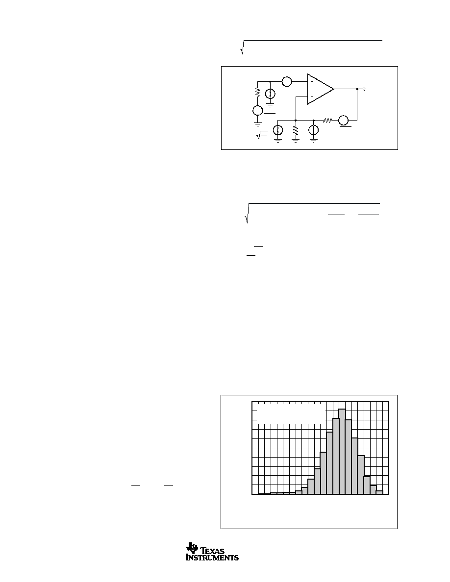
NOISE PERFORMANCE
The OPA843 complements its ultra low harmonic distortion
with low input noise terms. Both the input-referred voltage
noise, and the two input-referred current noise terms com-
bine to give a low output noise under a wide variety of
operating conditions. Figure 12 shows the op amp noise
analysis model with all the noise terms included. In this
model, all the noise terms are taken to be noise voltage or
current density terms in either nV/
Hz or pA/
Hz.
The total output spot noise voltage is computed as the square
root of the squared contributing terms to the output noise
voltage. This computation is adding all the contributing noise
powers at the output by superposition, and then taking the
square root to get back to a spot noise voltage. Equation 15
shows the general form for this output noise voltage using the
terms presented in Figure 12.
E
E
I
R
kTR
NG
I R
kTR NG
O
NI
BN
S
S
BI F
F
=
+
(
)
+
(
)
+
(
)
+
2
2
2
2
4
4
(15)
Dividing this expression by the noise gain (NG = 1 + R
F
/R
G
)
will give the equivalent input referred spot noise voltage at
the noninverting input, as shown in Equation 16.
E
E
I
R
kTR
I R
NG
kTR
NG
N
NI
BN
S
S
BI
F
F
=
+
(
)
+
+
+
2
2
2
4
4
(16)
Evaluating these two equations for the OPA843 circuit pre-
sented in Figure 1 will give a total output spot noise voltage
of 12.4nV/
Hz and an equivalent input spot noise voltage of
2.48nV/
Hz.
DC OFFSET CONTROL
The OPA843 can provide excellent DC signal accuracy due to
its high open-loop gain, high common-mode rejection, high
power supply rejection, and low input offset voltage and bias
current offset errors. To take full advantage of this low input
offset voltage, careful attention to input bias current cancella-
tion is also required. The high-speed input stage for the
OPA843 has a relatively high input bias current (20
µ
A typical
into the pins) but with a very close match between the two
input currents--typically 0.17
µ
A input offset current. Figures
13 and 14 show typical distribution of input offset voltage and
current for the OPA843.
mV
<
1.20
<
1.08
Count
1000
900
800
700
600
500
400
300
200
100
0
<
0.96
<
0.84
<
0.72
<
0.60
<
0.48
<
0.36
<
0.24
<
0.12
<
0.00
<0.12
<0.24
<0.36
<0.48
<0.60
<0.72
<0.84
<0.96
<1.08
<1.20
>1.20
Mean = 0.38mV
Standard Deviation = 0.31mV
Total Count = 5572
FIGURE 13. Input Offset Voltage Distributing in mV.
FIGURE 12. Op Amp Noise Analysis Model.
4kT
R
G
R
G
R
F
R
S
OPA843
I
BI
E
O
I
BN
4kT = 1.6E 20J
at 290
°
K
E
RS
E
NI
4kTR
S
4kTR
F
OPA843
17
SBOS268A
www.ti.com
The total output offset voltage may be considerably reduced
by matching the source impedances looking out of the two
inputs. For example, one way to add bias current cancellation
to the circuit of Figure 1 would be to insert a 55
series resistor
into the noninverting input from the 50
terminating resistor.
When the 50
source resistor is DC coupled, this will increase
the source impedance for the noninverting input bias current
to 80
. Since this is now equal to the impedance looking out
of the inverting input (R
F
|| R
G
), the circuit will cancel the gains
for the bias currents to the output leaving only the offset
current times the feedback resistor as a residual DC error term
at the output. Using a 402
feedback resistor, this output error
will now be less than 1
µ
A · 402
= 0.4mV at 25
°
C.
A fine-scale output offset null, or DC operating point adjust-
ment, is sometimes required. Numerous techniques are
available for introducing a DC offset control into an op amp
circuit. Most of these techniques eventually reduce to setting
up a DC current through the feedback resistor. One key
consideration to selecting a technique is to insure that it has
a minimal impact on the desired signal path frequency
response. If the signal path is intended to be noninverting,
the offset control is best applied as an inverting summing
signal to avoid interaction with the signal source. If the signal
path uses the inverting mode, applying an offset control to
the noninverting input can be considered. For a DC-coupled
inverting input signal, this DC offset signal will set up a DC
current back into the source that must be considered. An
offset adjustment placed on the inverting op amp input can
also change the noise gain and frequency response flatness.
Figure 15 shows one example of an offset adjustment for a
DC-coupled signal path that will have minimum impact on the
signal frequency response. In this case, the input is brought
into an inverting gain resistor with the DC adjustment an
additional current summed into the inverting node. The
resistor values for setting this offset adjustment are chosen
to be much larger than the signal path resistors. This will
insure that this adjustment has minimal impact on the loop
gain and hence, the frequency response.
THERMAL ANALYSIS
The OPA843 will not require heat sinking or airflow in most
applications. Maximum desired junction temperature would
set the maximum allowed internal power dissipation as
described below. In no case should the maximum junction
temperature be allowed to exceed +150
°
C.
Operating junction temperature (T
J
) is given by T
A
+ P
D
·
JA
.
The total internal power dissipation (P
D
) is the sum of quiescent
power (P
DQ
) and additional power dissipated in the output
stage (P
DL
) to deliver load power. Quiescent power is simply
the specified no-load supply current times the total supply
voltage across the part. P
DL
will depend on the required output
signal and load but would, for a grounded resistive load, be at
a maximum when the output is fixed at a voltage equal to 1/2
of either supply voltage (for equal bipolar supplies). Under this
worst-case condition, P
DL
= V
S
2
/(4 · R
L
), where R
L
includes
feedback network loading.
Note that it is the power in the output stage and not in the
load that determines internal power dissipation.
As a worst-case example, compute the maximum T
J
using an
OPA843IDBV (SOT23-5 package) in the circuit of Figure 1
operating at the maximum specified ambient temperature of
+85
°
C. P
D
= 10V(22.5mA) + 5
2
/(4 · (100
|| 500
)) = 300mW.
Maximum T
J
= +85
°
C + (0.30W · 150
°
C/W) = 130
°
C.
mV
<
1.00
<
0.90
Count
1600
1400
1200
1000
800
600
400
200
0
<
0.80
<
0.70
<
0.60
<
0.50
<
0.40
<
0.30
<
0.20
<
0.10
<
0.00
<0.10
<0.20
<0.30
<0.40
<0.50
<0.60
<0.70
<0.80
<1.90
<1.00
>1.00
Mean = 0.04
µ
A
Standard Deviation = 0.17
µ
A
Total Count = 5572
FIGURE 14.
R
F
1k
±
125mV Output Adjustment
= = 4
Power-supply decoupling
not shown.
5k
5k
200
0.1
µ
F
R
G
250
V
IN
20k
10k
0.1
µ
F
5V
+5V
OPA843
+5V
V
CC
V
EE
5V
V
O
V
O
V
IN
R
F
R
G
FIGURE 15. DC Coupled, Inverting Gain of 4 with Output
Offset Adjustment.

OPA843
18
SBOS268A
www.ti.com
BOARD LAYOUT
Achieving optimum performance with a high-frequency am-
plifier such as the OPA843 requires careful attention to board
layout parasitics and external component types. Recommen-
dations that will optimize performance include:
a) Minimize parasitic capacitance to any AC ground for
all of the signal I/O pins. Parasitic capacitance on the
output and inverting input pins can cause instability: on the
noninverting input, it can react with the source impedance to
cause unintentional bandlimiting. To reduce unwanted ca-
pacitance, a window around the signal I/O pins should be
opened in all of the ground and power planes around those
pins. Otherwise, ground and power planes should be unbro-
ken elsewhere on the board.
b) Minimize the distance (< 0.25") from the power-supply
pins to high-frequency 0.1
µ
F decoupling capacitors. At
the device pins, the ground and power-plane layout should
not be in close proximity to the signal I/O pins. Avoid narrow
power and ground traces to minimize inductance between
the pins and the decoupling capacitors. The power-supply
connections should always be decoupled with these capaci-
tors. Larger (2.2
µ
F to 6.8
µ
F) decoupling capacitors, effective
at lower frequency, should also be used on the main supply
pins. These may be placed somewhat farther from the device
and may be shared among several devices in the same area
of the PC board.
c) Careful selection and placement of external compo-
nents will preserve the high-frequency performance of
the OPA843. Resistors should be a very low reactance type.
Surface-mount resistors work best and allow a tighter overall
layout. Metal-film and carbon composition, axially-leaded
resistors can also provide good high-frequency performance.
Again, keep their leads and PC board trace length as short
as possible. Never use wire-wound type resistors in a high-
frequency application. Since the output pin and inverting
input pin are the most sensitive to parasitic capacitance,
always position the feedback and series output resistor, if
any, as close as possible to the output pin. Other network
components, such as noninverting input termination resis-
tors, should also be placed close to the package. Where
double-feedback side component mounting is allowed, place
the feedback resistor directly under the package on the other
side of the board between the output and inverting input pins.
Even with a low parasitic capacitance shunting the external
resistors, excessively high resistor values can create signifi-
cant time constants that can degrade performance. Good
axial metal-film or surface-mount resistors have approxi-
mately 0.2pF in shunt with the resistor. For resistor values
> 1.5k
, this parasitic capacitance can add a pole and/or a
zero below 500MHz that can effect circuit operation. Keep
resistor values as low as possible consistent with load driving
considerations.
d) Connections to other wideband devices on the board
may be made with short, direct traces or through onboard
transmission lines. For short connections, consider the
trace and the input to the next device as a lumped capacitive
load. Relatively wide traces (50mils to 100mils) should be
used, preferably with ground and power planes opened up
around them. Estimate the total capacitive load and set R
S
from the plot of recommended "R
S
vs Capacitive Load." Low
parasitic capacitive loads (< 5pF) may not need an R
S
since
the OPA843 is nominally compensated to operate with a 2pF
parasitic load. Higher parasitic capacitive loads without an R
S
are allowed as the signal gain increases (increasing the
unloaded phase margin). If a long trace is required, and the
6dB signal loss intrinsic to a doubly-terminated transmission
line is acceptable, implement a matched-impedance trans-
mission line using microstrip or stripline techniques (consult
an ECL design handbook for microstrip and stripline layout
techniques). A 50
environment is normally not necessary
on board, and in fact a higher impedance environment will
improve distortion as shown in the distortion versus load
plots. With a characteristic board trace impedance defined
based on board material and trace dimensions, a matching
series resistor into the trace from the output of the OPA843
is used as well as a terminating shunt resistor at the input of
the destination device. Remember also that the terminating
impedance will be the parallel combination of the shunt
resistor and input impedance of the destination device; this
total effective impedance should be set to match the trace
impedance. If the 6dB attenuation of a doubly-terminated
transmission line is unacceptable, a long trace can be series-
terminated at the source end only. Treat the trace as a
capacitive load in this case and set the series resistor value
as shown in the plot of "R
S
vs Capacitive Load." This will not
preserve signal integrity as well as a doubly-terminated line.
If the input impedance of the destination device is low, there
will be some signal attenuation due to the voltage divider
formed by the series output into the terminating impedance.
e) Socketing a high-speed part like the OPA843 is not
recommended. The additional lead length and pin-to-pin
capacitance introduced by the socket can create an ex-
tremely troublesome parasitic network, which can make it
almost impossible to achieve a smooth, stable frequency
response. Best results are obtained by soldering the OPA843
onto the board.
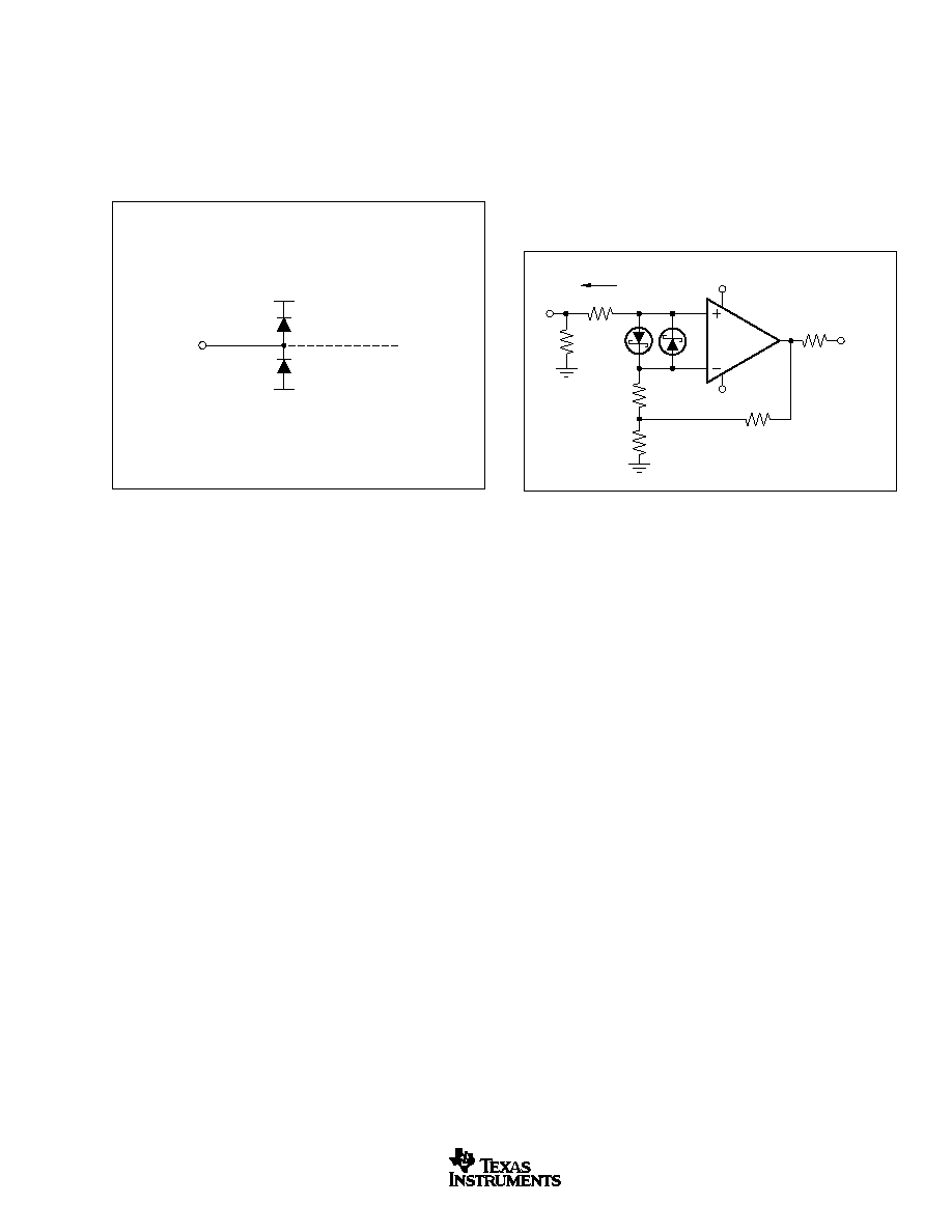
OPA843
19
SBOS268A
www.ti.com
INPUT AND ESD PROTECTION
The OPA843 is built using a very high-speed complementary
bipolar process. The internal junction breakdown voltages are
relatively low for these very small geometry devices. These
breakdowns are reflected in the Absolute Maximum Ratings
table. All device pins are protected with internal ESD protec-
tion diodes to the power supplies, as shown in Figure 16.
These diodes provide moderate protection to input overdrive
voltages above the supplies as well. The protection diodes
can typically support 30mA continuous current. Where higher
currents are possible (e.g., in systems with
±
15V supply parts
driving into the OPA843), current-limiting series resistors
should be added into the two inputs. Keep these resistor
values as low as possible since high values degrade both
noise performance and frequency response. Figure 17 shows
one example of an overdrive protection circuit added to a
G = +5V/V design.
External
Pin
Internal
Cicuitry
+V
CC
V
CC
OPA843
+5V
5V
50
50
Power-supply
decoupling not shown.
125
D1
D2
R
G
126
50
R
F
505
V
O
D1 = D2 IN5911 (or equivalent)
50
Source
FIGURE 17. Gain of +5 with Input Protection.
FIGURE 16. Internal ESD Protection.
OPA843
20
SBOS268A
www.ti.com
D (R-PDSO-G**)
PLASTIC SMALL-OUTLINE PACKAGE
8 PINS SHOWN
8
0.197
(5,00)
A MAX
A MIN
(4,80)
0.189
0.337
(8,55)
(8,75)
0.344
14
0.386
(9,80)
(10,00)
0.394
16
DIM
PINS **
4040047/E 09/01
0.069 (1,75) MAX
Seating Plane
0.004 (0,10)
0.010 (0,25)
0.010 (0,25)
0.016 (0,40)
0.044 (1,12)
0.244 (6,20)
0.228 (5,80)
0.020 (0,51)
0.014 (0,35)
1
4
8
5
0.150 (3,81)
0.157 (4,00)
0.008 (0,20) NOM
0
°
8
°
Gage Plane
A
0.004 (0,10)
0.010 (0,25)
0.050 (1,27)
NOTES: A. All linear dimensions are in inches (millimeters).
B. This drawing is subject to change without notice.
C. Body dimensions do not include mold flash or protrusion, not to exceed 0.006 (0,15).
D. Falls within JEDEC MS-012
PACKAGE DRAWINGS
OPA843
21
SBOS268A
www.ti.com
DBV (R-PDSO-G5)
PLASTIC SMALL-OUTLINE
0,10
M
0,20
0,95
0
°
8
°
0,25
0,35
0,55
Gage Plane
0,15 NOM
4073253-4/G 01/02
2,60
3,00
0,50
0,30
1,50
1,70
4
5
3
1
2,80
3,00
0,95
1,45
0,05 MIN
Seating Plane
NOTES: A. All linear dimensions are in millimeters.
B. This drawing is subject to change without notice.
C. Body dimensions do not include mold flash or protrusion.
D. Falls within JEDEC MO-178
PACKAGE DRAWINGS (Cont.)

IMPORTANT NOTICE
Texas Instruments Incorporated and its subsidiaries (TI) reserve the right to make corrections, modifications,
enhancements, improvements, and other changes to its products and services at any time and to discontinue
any product or service without notice. Customers should obtain the latest relevant information before placing
orders and should verify that such information is current and complete. All products are sold subject to TI's terms
and conditions of sale supplied at the time of order acknowledgment.
TI warrants performance of its hardware products to the specifications applicable at the time of sale in
accordance with TI's standard warranty. Testing and other quality control techniques are used to the extent TI
deems necessary to support this warranty. Except where mandated by government requirements, testing of all
parameters of each product is not necessarily performed.
TI assumes no liability for applications assistance or customer product design. Customers are responsible for
their products and applications using TI components. To minimize the risks associated with customer products
and applications, customers should provide adequate design and operating safeguards.
TI does not warrant or represent that any license, either express or implied, is granted under any TI patent right,
copyright, mask work right, or other TI intellectual property right relating to any combination, machine, or process
in which TI products or services are used. Information published by TI regarding third-party products or services
does not constitute a license from TI to use such products or services or a warranty or endorsement thereof.
Use of such information may require a license from a third party under the patents or other intellectual property
of the third party, or a license from TI under the patents or other intellectual property of TI.
Reproduction of information in TI data books or data sheets is permissible only if reproduction is without
alteration and is accompanied by all associated warranties, conditions, limitations, and notices. Reproduction
of this information with alteration is an unfair and deceptive business practice. TI is not responsible or liable for
such altered documentation.
Resale of TI products or services with statements different from or beyond the parameters stated by TI for that
product or service voids all express and any implied warranties for the associated TI product or service and
is an unfair and deceptive business practice. TI is not responsible or liable for any such statements.
Following are URLs where you can obtain information on other Texas Instruments products and application
solutions:
Products
Applications
Amplifiers
amplifier.ti.com
Audio
www.ti.com/audio
Data Converters
dataconverter.ti.com
Automotive
www.ti.com/automotive
DSP
dsp.ti.com
Broadband
www.ti.com/broadband
Interface
interface.ti.com
Digital Control
www.ti.com/digitalcontrol
Logic
logic.ti.com
Military
www.ti.com/military
Power Mgmt
power.ti.com
Optical Networking
www.ti.com/opticalnetwork
Microcontrollers
microcontroller.ti.com
Security
www.ti.com/security
Telephony
www.ti.com/telephony
Video & Imaging
www.ti.com/video
Wireless
www.ti.com/wireless
Mailing Address:
Texas Instruments
Post Office Box 655303 Dallas, Texas 75265
Copyright
2003, Texas Instruments Incorporated
Document Outline
- FEATURES
- APPLICATIONS
- DESCRIPTION
- ABSOLUTE MAXIMUM RATINGS(
- PACKAGE/ORDERING INFORMATION
- PIN CONFIGURATIONS
- ELECTRICAL CHARACTERISTICS: VS = ±5V
- TYPICAL CHARACTERISTICS: VS = ±5V
- APPLICATIONS INFORMATION
- WIDEBAND NONINVERTING OPERATION
- WIDEBAND, INVERTING GAIN OPERATION
- BUFFERING HIGH-PERFORMANCE ADCs
- WIDE DYNAMIC RANGE ÏIF AMPLIFIER
- WIDEBAND INVERTING SUMMING AMPLIFIER
- 2nd-Order Filter Topology
- EQUALIZING FILTER APPLICATION
- PHOTODIODE TRANSIMPEDANCE AMPLIFIER
- DESIGN-IN TOOLS
- DEMONSTRATION BOARDS
- MACROMODELS AND APPLICATIONS SUPPORT
- OPERATING SUGGESTIONS
- OPTIMIZING RESISTOR VALUES
- BANDWIDTH vs GAIN
- LOW GAIN OPERATION
- OUTPUT DRIVE CAPABILITY
- DRIVING CAPACITIVE LOADS
- DISTORTION PERFORMANCE
- NOISE PERFORMANCE
- DC OFFSET CONTROL
- THERMAL ANALYSIS
- BOARD LAYOUT
- INPUT AND ESD PROTECTION
- PACKAGE DRAWINGS
- D (R-PDSO-G**) PLASTIC SMALL-OUTLINE PACKAGE
- DBV (R-PDSO-G5) PLASTIC SMALL-OUTLINE
- IMPORTANT NOTICE