 | –≠–ª–µ–∫—Ç—Ä–æ–Ω–Ω—ã–π –∫–æ–º–ø–æ–Ω–µ–Ω—Ç: PCM1710 | –°–∫–∞—á–∞—Ç—å:  PDF PDF  ZIP ZIP |

49%
FPO
Stereo Audio
DIGITAL-TO-ANALOG CONVERTER
PCM1710U
Æ
FEATURES
q
COMPLETE STEREO DAC:
8X Oversampling Digital Filter
Multi-Level Delta-Sigma DAC
Analog Low Pass Filter
Output Amplifier
q
HIGH PERFORMANCE:
≠92dB THD+N
98dB Dynamic Range
110dB SNR
q
ACCEPTS 16 OR 20 BITS INPUT DATA
q
SYSTEM CLOCK: 256fs or 384fs
q
SINGLE +5V POWER SUPPLY
q
ON-CHIP DIGITAL FILTER:
Soft Mute and Attenuator
Digital De-emphasis
Double-Speed Dubbing Mode
q
SMALL 28-PIN SOIC PACKAGE
DESCRIPTION
The PCM1710 is a complete stereo audio digital-to-
analog converter, including digital interpolation filter,
delta-sigma DAC, and analog voltage output. PCM1710
can accept either 16-bit normal or 20-Bit normal input
data (MSB first, right justified), or 16-bit IIS data
(32-bits per word, continuous clock).
The digital filter performs an 8X interpolation func-
tion, as well as special functions such as soft mute,
digital attenuation, de-emphasis and double-speed
dubbing. Performance of the digital feature is excel-
lent, featuring ≠62dB stop band attenuation and
±
0.008dB ripple in the pass band.
PCM1710 is suitable for a wide variety of consumer
applications where good performance is required.
Its low cost, small size and single +5V power supply
make it ideal for automotive CD players, bookshelf
CD players, BS tuners, keyboards, MPEG audio,
MIDI applications, set-top boxes, CD-ROM drives,
CD-Interactive and CD-Karaoke systems.
International Airport Industrial Park ∑ Mailing Address: PO Box 11400 ∑ Tucson, AZ 85734 ∑ Street Address: 6730 S. Tucson Blvd. ∑ Tucson, AZ 85706
Tel: (520) 746-1111 ∑ Twx: 910-952-1111 ∑ Cable: BBRCORP ∑ Telex: 066-6491 ∑ FAX: (520) 889-1510 ∑ Immediate Product Info: (800) 548-6132
Digital In
Input Interface
and
Attentuator
Oversampling
Digital Filter
4th-Order
Multi-Level
Delta
Sigma
DAC
Low-Pass
Filter
Output
Op Amp
Mode Control
System Clock
Lch OUT
Rch OUT
© 1994 Burr-Brown Corporation
PDS-1217B
Printed in U.S.A. June, 1995
Æ
PCM1710U
2
SPECIFICATIONS
All specifications at +25
∞
C, +V
CC
= +V
DD
= +5V, f
S
= 44.1kHz, f
SYS
= 384/256fs, and 16-bit data, unless otherwise noted.
The information provided herein is believed to be reliable; however, BURR-BROWN assumes no responsibility for inaccuracies or omissions. BURR-BROWN assumes
no responsibility for the use of this information, and all use of such information shall be entirely at the user's own risk. Prices and specifications are subject to change
without notice. No patent rights or licenses to any of the circuits described herein are implied or granted to any third party. BURR-BROWN does not authorize or warrant
any BURR-BROWN product for use in life support devices and/or systems.
PCM1710U
PARAMETER
CONDITIONS
MIN
TYP
MAX
UNITS
RESOLUTION
16
20
Bits
DIGITAL INPUT
Logic Family
Input Logic Level (except XTI)
V
IH
2.0
VDC
V
IL
0.8
VDC
Input Logic Current (except XTI)
≠200
µ
A
Input Logic Level (XTI)
V
IH
3.2
VDC
V
IL
1.4
VDC
Input Logic Current (XTI)
±
50
µ
A
Output Logic Level (CLKO):
V
OH
4.5
VDC
V
OL
0.5
VDC
Output Logic Current (CLKO)
±
10
mA
Data Format
Normal (16/20-bit)/IIS (16-bit) selectable
Sampling Frequency
32
44.1
48
kHz
System Clock Frequency
384f
S
12.288
16.934
18.432
MHz
System Clock Frequency
256f
S
8.192
11.2894
12.288
MHz
DC ACCURACY
Gain Error
±
1.0
±
5.0
% of FSR
Gain Mis-Match Channel-To-Channel
±
1.0
±
5.0
% of FSR
Bipolar Zero Error
V
O
= 1/2V
CC
at Bipolar Zero
±
20.0
mV
Gain Drift
±
50
ppm of FSR/
∞
C
Bipolar Gain Drift
±
20
ppm of FSR/
∞
C
DYNAMIC PERFORMANCE
(1)
THD+N at F/S (0dB)
(2)
f
IN
= 991kHz
≠92
≠88
dB
THD+N at ≠60fdB
(2)
f
IN
= 991kHz
≠36
≠32
dB
Dynamic Range
EIAJ A-weighted
98
dB
S/N Ratio
EIAJ A-weighted
104
110
dB
Channel Separation
90
94
dB
DIGITAL FILTER PERFORMANCE
Pass Band Ripple
Normal Mode
±
0.008
dB
Pass Band Ripple
Double Speed Mode
±
0.018
dB
Stop Band Attenuation
Normal Mode
≠62
dB
Stop Band Attenuation
Double Speed Mode
≠58
dB
Pass Band
Normal Mode
0.4535
fs
Pass Band
Double Speed Mode
0.4535
fs
Stop Band
Normal Mode
0.5465
fs
Stop Band
Double Speed Mode
0.5465
fs
De-emphasis Error
(f
S
32kHz ~ 48kHz)
≠0.05
+0.03
dB
ANALOG OUTPUT
Voltage Range
3.2
Vp-p
Load Impedance
5
k
Center Voltage
+1/2V
CC
V
POWER SUPPLY REQUIREMENTS
Voltage Range: +V
CC
+4.5
+5.0
+5.5
VDC
+V
DD
+4.5
+5.0
+5.5
VDC
Supply Current (+I
CC
) + (+I
DD
)
45
70
mA
TEMPERATURE RANGE
Operation
≠25
+85
∞
C
Storage
≠55
+100
∞
C
NOTE: (1) Dynamic performance specs are tested with external 20kHz low pass filter. (2) 30kHz LPF, 400Hz HPF, Average Mode. Shibusoku #725 THD Meter.
3
Æ
PCM1710U
PIN ASSIGNMENTS
PIN NAME
NUMBER
FUNCTION
Input Interface Pins
LRCIN
1
Sample Rate Clock Input. Controls the update rate (fs).
DIN
2
Serial Data Input. MSB first, right justified format contains a frame of 16-bit or 20-bit data.
BCKIN
3
Bit Clock Input. Clocks in the data present on DIN input.
Mode Controls and Clock Signals
CLKO
4
Buffered Output of Oscillator. Equivalent to fs.
XTI
5
Oscillator Input (External Clock Input). For an internal clock, tie XTI to one side of the crystal oscillator. For an external clock,
tie XTI to the output of the chosen external clock.
XTO
6
Oscillator Output. When using the internal clock, tie to the opposite side (from pin 5) of the crystal oscillator. When using an
external clock, leave XTO open.
CKSL
23
System Clock Select. For 384fs, tie CKSL "High". For 256fs, tie CKSL "Low".
MODE
24
Operation Mode Select. For serial mode, tie MODE "High". For parallel mode, tie MODE "Low".
MUTE
25
Mute Control. To disable soft mute, tie MUTE "High". To enable soft mute, tie MUTE "Low".
MD/DM1
26
Mode Control for Data/De-emphasis. See "Mode Control Functions" on page 11.
MC/DM2
27
Mode Control for BCKIN/De-emphasis. See "Mode Control Functions" on page 11.
ML/DSD
28
Mode Control for WDCK/Double speed dubbing. See "Mode Control Functions" on page 11.
Analog Functions
V
OUT
R
13
Right Channel Analog Output.
V
OUT
L
16
Left Channel Analog Output.
Power Supply Connections
DGND
7, 22
Digital Ground.
V
DD
8, 21
Digital Power Supply (+5V).
V
CC
2R
9
Analog Power Supply (+5V), Right Channel DAC.
AGND2R
10
Analog Ground (DAC), Right Channel.
EXT1R
11
Output Amplifier Common, Right Channel. Bypass to ground with a 10
µ
F capacitor.
EXT2R
12
Output Amplifier Bias, Right Channel. Connect to EXT1R.
AGND
14
Analog Ground.
V
CC
15
Analog Power Supply (+5V).
EXT2L
17
Output Amplifier Bias, Left Channel. Connect to EXT1L.
EXT1L
18
Output Amplifier Common, Left Channel. Bypass to ground with a 10
µ
F capacitor.
AGND2L
19
Analog Ground (DAC), Left Channel.
V
CC
2L
20
Analog Power Supply (+5V), Left Channel DAC.
Power Supply Voltages ................................................................
±
6.5VDC
+V
CC
to V
DD
Voltage ..........................................................................
±
0.1V
Input Logic Voltage ..................................................... ≠0.3V to V
DD
+0.3V
Power Dissipation .......................................................................... 400mW
Operating Temperature Range ......................................... ≠25
∞
C to +85
∞
C
Storage Temperature Range .......................................... ≠55
∞
C to +125
∞
C
Lead Temperature (soldering, 5s) ................................................. +260
∞
C
ABSOLUTE MAXIMUM RATINGS
PACKAGE INFORMATION
PACKAGE DRAWING
MODEL
PACKAGE
NUMBER
(1)
PCM1710U
28-Pin SOIC
217
NOTE: (1) For detailed drawing and dimension table, please see end of data
sheet, or Appendix D of Burr-Brown IC Data Book.
Æ
PCM1710U
4
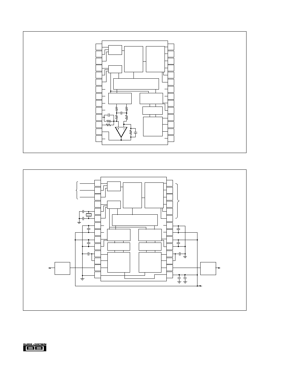
PIN CONFIGURATION
CONNECTION DIAGRAM
1
2
3
4
5
6
7
8
9
10
11
12
13
14
28
27
26
25
24
23
22
21
20
19
18
17
16
15
Input
Interface
Digital
Filter
Mode
Control
Timing
Control
Noise
Shaper
5-Level
DAC
Right
5-Level
DAC
Left
Low-Pass
Filter Left
Output
Amplifier
Left
Serial
Data Input
(2)
Mode Control
(3)
Low-Pass
Filter Right
Output
Amplifier
Right
NOTES: (1) Bypass Capacitor :1µF ~ 10µF.
(2) Input pins require pull-up resistors. (3) Mode
control pins require pull-up resistors.
10pF ~ 22pF x 2
10µF
Rch OUT
Lch OUT
+5V
Power Supply
10µF
100µF
+
+
+
≠
(1)
(1)
(1)
(1)
(1)
Post
Low Pass
Filter
Post
Low Pass
Filter
LRCIN
DIN
BCKIN
CLKO
XTI
XTO
DGND
V
DD
V
CC
2R
AGND2R
EXT1R
EXT2R
V
OUT
R
AGND1
ML/DSD
MC/DM2
MD/DM1
MUTE
MODE
CKSL
DGND
V
DD
V
CC
2L
AGND2L
EXT1L
EXT2L
V
OUT
L
V
CC
1
1
2
3
4
5
6
7
8
9
10
11
12
13
14
28
27
26
25
24
23
22
21
20
19
18
17
16
15
Input
Interface
Digital
Filter
Mode
Control
Timing
Control
Noise
Shaper
5-Level
DAC
Right
5-Level
DAC
Left
Low-Pass
Filter-Left
Output
Amplifier
Left

5
Æ
PCM1710U
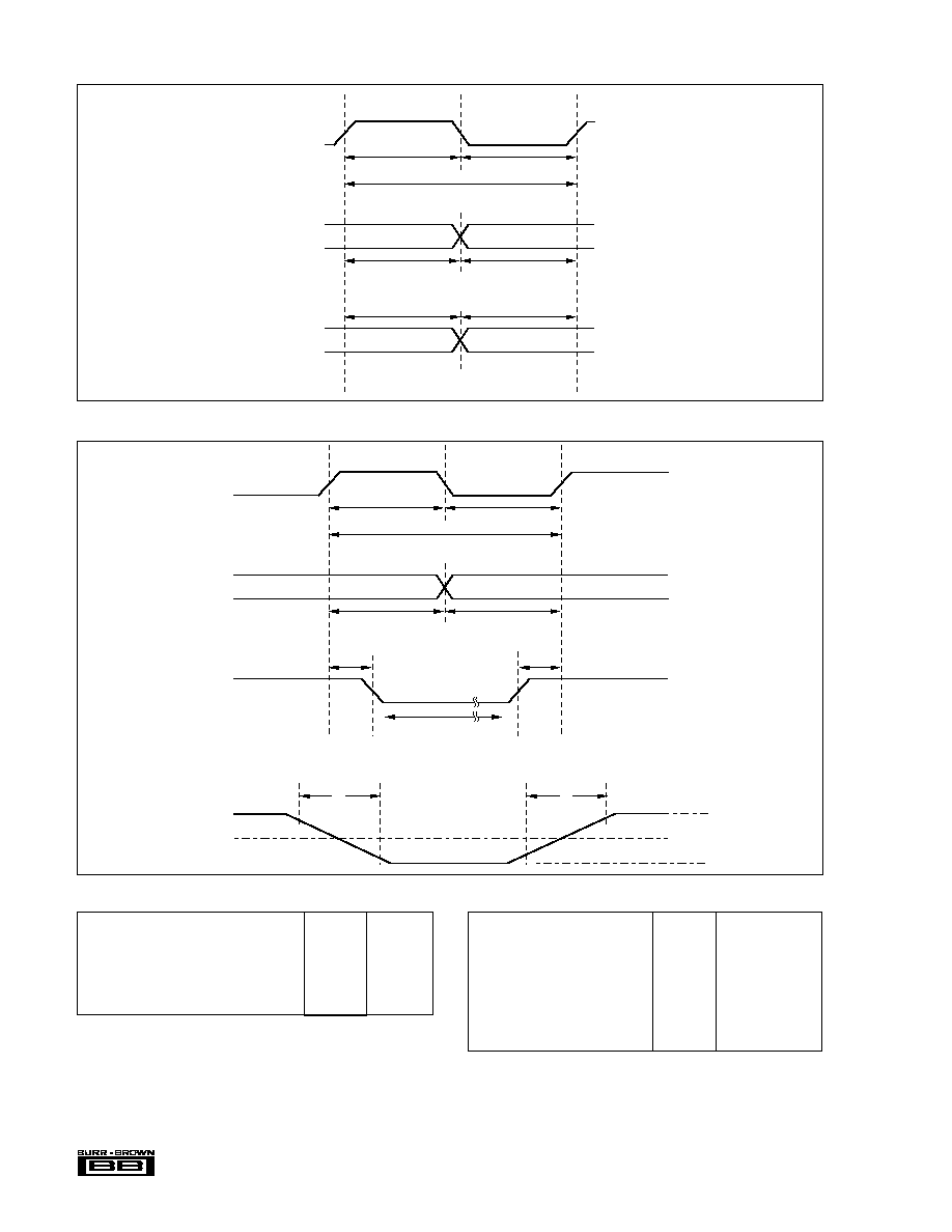
DATA INPUT TIMING
1
LRCIN
DIN
BCKIN
2
14
16
15
1
2
14
16
15
MSB
LSB
MSB
LSB
Left-channel Data
Right-channel Data
1 f/s
FIGURE 1. Normal Format, 16-Bit (LRCIN H: Lch).
FIGURE 2. Normal Format, 20-Bit (LRCIN H: Lch).
FIGURE 3. IIS Format, (16-Bit, 32 BCKIN Clock Cycles Per fs Interval).
1
LRCIN
DIN
BCKIN
2
18
20
19
1
2
18
20
19
MSB
LSB
MSB
LSB
Left-channel Data
Right-channel Data
1 f/s
1
LRCIN
DIN
BCKIN
2
13
16
14
1
2
13
15
14
MSB
LSB MSB
LSB
Left-channel Data
Right-channel Data
1 f/s
15
16
16
3
Æ
PCM1710U
6
FIGURE 4. Data Input Timing.
FIGURE 5. Serial Mode Control Timing.
BCK Pulsewidth (H Level)
t
BCWH
70ns (min)
BCK Pulsewidth (L Level)
t
BCWL
70ns (min)
BCK Pulse Cycle Time
t
BCY
140ns (min)
DIN Setup Time
t
DS
30ns (min)
DIN Hold Time
t
DH
30ns (min)
BCK Rising Edge
®
LRCI Edge
t
BL
30ns (min)
LRC I Edge
®
BCK Rising Edge
t
LB
30ns (min)
MC Pulsewidth (H Level)
t
MCWH
50ns (min)
MC Pulsewidth (L Level)
t
MCWL
50ns (min)
MC Pulse Cycle Time
t
MCY
100ns (min)
MD Setup Time
t
MS
30ns (min)
MD Hold Time
t
MH
30ns (min)
ML Setup Time
t
MCS
30ns (min)
ML Hold Time
t
MCH
30ns (min)
ML Low-Level Time
t
MLY
1/sysclk + 20ns (min)
MC, MD, ML Rise Time
t
R
15ns (max)
MC, MD, ML Fall Time
t
F
15ns (max)
TABLE I. Data Input Timing Specifications (Refer to
Figure 4).
t
BCWH
t
BCWL
t
BCY
t
DH
t
DS
t
BL
t
LB
BCKIN
DIN
LRCIN
TABLE II. Serial Mode Control Timing Specifications
(Refer to Figure 5).
t
MCWH
t
MCWL
t
MCY
t
MH
t
MS
t
MCS
t
MCH
MC
MD
ML
MC, MD, ML
0.8V
2.0V
t
MLY
t
F
t
R
7
Æ
PCM1710U
DE-EMPHASIS CHARACTERISTIC, NORMAL MODE
0
≠2
≠4
≠6
≠8
≠10
≠12
0
5k
10k
15k
20k
25k
dB
Frequency (Hz)
DE-EMPHASIS CHARACTERISTIC
DOUBLE-SPEED MODE
0
≠2
≠4
≠6
≠8
≠10
≠12
0
10k
20k
30k
40k
50k
dB
Frequency (Hz)
TYPICAL PERFORMANCE CURVES
All specifications at +25
∞
C, +V
CC
= + V
DD
+ 5V, f
S
= 44.1kHz, f
SYS
= 384/256fs, and 16-bit data, unless otherwise noted.
DIGITAL FILTER
0
20k
40k
60k
80k
100k 120k 140k
180k
0
≠20
≠40
≠60
≠80
≠100
≠120
≠140
dB
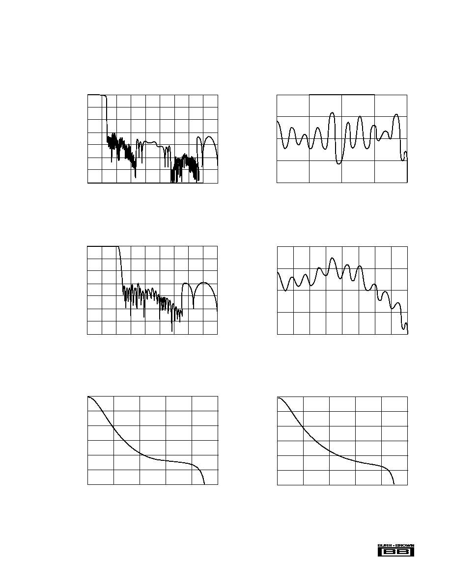
OVERALL FREQUENCY CHARACTERISTIC
NORMAL MODE (De-emphasis: OFF)
Frequency (Hz)
160k
0
20k
40k
60k
80k
100k 120k 140k 160k 180k
0
≠20
≠40
≠60
≠80
≠100
≠120
≠140
dB
OVERALL FREQUENCY CHARACTERISTIC
DOUBLE-SPEED MODE (De-emphasis: OFF)
Frequency (Hz)
PASSBAND RIPPLE FREQUENCY CHARACTERISTIC
DOUBLE-SPEED MODE (De-emphasis: OFF)
≠0.02
≠0.03
≠0.04
≠0.05
≠0.06
0
5k
10k
15k
20k
25k
30k
35k
40k
dB
Frequency (Hz)
PASSBAND RIPPLE CHARACTERISTIC
NORMAL MODE (De-emphasis: OFF)
≠0.03
≠0.035
≠0.04
≠0.045
≠0.05
0
5k
10k
15k
20k
dB
Frequency (Hz)

Æ
PCM1710U
8
15
13
11
9
7
5
3
1
≠1
≠3
≠5
≠7
≠9
≠11
≠13
≠15
384fs
BPZ ERROR vs V
CC
, V
DD
V
CC
, V
DD
(V)
4.5
5
5.5
Average
Minimum
BPZ Error (mV)
Maximum
2.0
1.8
1.6
1.4
1.2
1
0.8
0.6
0.4
0.2
0
384fs
GAIN ERROR vs V
CC
, V
DD
V
CC
, V
DD
(V)
4.5
5
5.5
Maximum
Average
Minimum
Gain Error (%)
92
93
94
95
96
97
98
99
384fs
DYNAMIC RANGE vs V
CC
, V
DD
V
CC,
V
DD
(V)
4.5
5.0
5.5
Dynamic Range (dB)
Average
Minimum
Maximum
91
92
93
94
95
96
97
98
256fs
DYNAMIC RANGE vs V
CC
, V
DD
V
CC,
V
DD
(V)
4.5
5.0
5.5
Dynamic Range (dB)
Average
Maximum
Minimum
≠89
≠90
≠91
≠92
≠93
≠94
≠95
≠96
384fs
THD+N vs V
CC
, V
DD
FULL SCALE INPUT
V
CC,
V
DD
(V)
4.5
5.0
5.5
THD+N (dB)
Maximum
Average
Minimum
≠88
≠89
≠90
≠91
≠92
≠93
≠94
≠95
256fs
THD+N vs V
CC
, V
DD
FULL-SCALE INPUT
V
CC,
V
DD
(V)
4.5
5.0
5.5
THD+N (dB)
Maximum
Average
Minimum
At T
A
= +25
∞
C, V
S
=
±
5V, R
L
= 100
, C
L
= 2pF, and R
FB
= 402
, unless otherwise noted. Based on 200 piece sample from 3 diffusion runs.
DYNAMIC PERFORMANCE
TYPICAL PERFORMANCE CURVES
(CONT)

9
Æ
PCM1710U
INTERMODULATION DISTORTION
vs FREQUENCY (f
1
= 60Hz, f
2
= 7kHz)
20
100
1k
10k
20k
Frequency (Hz)
IMD (dB)
0
≠20
≠40
≠60
≠80
≠100
≠120
≠140
111
110
109
108
107
106
105
104
384fs
SNR vs TEMPERATURE and POWER SUPPLY
Temperature (∞C)
≠25
0
50
25
75
SNR (dB)
V
CC
, V
DD
= 4.5V
V
CC
, V
DD
= 5.0V
V
CC
, V
DD
= 5.5V
TYPICAL PERFORMANCE CURVES
(CONT)
At T
A
= +25
∞
C, V
S
=
±
5V, R
L
= 100
, C
L
= 2pF, and R
FB
= 402
, unless otherwise noted. Based on 200 piece sample from 3 diffusion runs.
DYNAMIC PERFORMANCE
CAUTION: Minimum and maximum values on typical performance curves are not meant to imply a guarantee. Curves should
be used for reference only. Refer to specification for guaranteed performances.
INTERMODULATION DISTORTION
vs FREQUENCY (f
1
= 11kHz, f
2
= 12kHz)
20
100
1k
10k
20k
Frequency (Hz)
IMD (dB)
0
≠20
≠40
≠60
≠80
≠100
≠120
≠140
Æ
PCM1710U
10
FUNCTIONAL DESCRIPTION
PCM1710 has several built-in functions including digital
attenuation, digital de-emphasis and soft mute. These func-
tions are software controlled. PCM1710 can be operated in
two different modes, Serial or Parallel. Serial Mode is a
three-wire interface using pin 26 (MD), pin 27 (MC), and pin
28 (ML). Data on these pins are used to control de-emphasis
mode, mute, double-speed dubbing, input resolution and
input format. PCM1710 can also be operated in parallel
mode, where static control signals are used on pin 26 (DM1),
pin 27 (DM2), and pin 28 (DSD). Operation of both of these
modes are covered in detail in the next sections.
CAUTION: Mode control signals operate on level triggered
logic. The minimum timing conditions detailed in Figures 5
and 6 MUST be observed.
DM1 (Pin 26)
DM2 (Pin 27)
De-emphasis
L
L
OFF
H
L
32kHz
L
H
48kHz
H
H
44.1kHz
PARALLEL-MODE: DE-EMPHASIS CONTROL
(PIN 24 [MODE] = L)
TABLE V. De-emphasis (Pins 26 and 27).
In the parallel mode, de-emphasis conditions are controlled
by the logic levels on pin 26 (DM1) and pin 27 (DM2). For
PCM1710, de-emphasis can operate at 32kHz, 44.1kHz,
48kHz, or disabled.
MODE CONTROL: SERIAL/PARALLEL SELECTION
MODE = H
Serial Mode
MODE = L
Parallel Mode
TABLE III. Serial and Parallel Mode are Selectable by
MODE Pin (Pin 24).
MODE CONTROL: SELECTABLE FUNCTIONS
TABLE IV. Selectable Functions in Serial Mode and
Parallel Mode.
SERIAL MODE
PARALLEL MODE
FUNCTION
(MODE = H)
(MODE = L)
Input Data Format Selection
0
X(Normal Mode Fixed)
Input Data Bit Selection
0
X(16-bit Fixed)
Input LRCI Polarity Selection
0
X
De-emphasis Control
0
0
Mute
0
0
Attenuation
0
X
Double Speed Dubbing
0
0
NOTE: 0: Selectable, X: Not Selectable.
Table IV indicates which functions are selectable within the
user's chosen mode. All of the functions shown are select-
able within the serial mode, but only de-emphasis control,
mute and double-speed dubbing may be selected when using
PCM1710 in the parallel mode.
PARALLEL-MODE: DOUBLE-SPEED DUBBING
CONTROL (PIN 24 [MODE] = L)
DSD = H
Normal Mode
DSD = L
Double-Speed Dubbing Mode
NOTE: When the Double-Speed Dubbing Mode is selected, the System
Clock must be 384fs (CKSL: Pin 23 = H).
TABLE VI. DSD (Pin 28).
In the parallel mode, double-speed dubbing can be enabled
by holding pin 28 (DSD) at a logic "low".
CAUTION: Double-speed dubbing cannot operate if the
system clock is set at 256fs.
SERIAL MODE CONTROL
In order to use all of PCM1710's functionality, the serial
mode control should be used. PCM1710 must be addressed
three separate times to set all of the various registers and
flags that control these functions.
Table VII together with Figure 6 details the control of the
PCM1710 in the serial mode. Internal latches are used to
hold this serial data until the PCM1710 is enabled to use the
data. The serial mode is used by applying clocked data to the
following pins:
NAME
PIN
FUNCTION
MC
27
Clock for Strobing in Data
ML
28
Latches Data into the Registers
MD
26
8-bit Data Word Defining Operation

11
Æ
PCM1710U
FUNCTION MODE SELECTION
B0
B1
B2
BIT NO.
FLAG
MODE
BIT VALUE
SELECTED FUNCTION
DEFAULT
B3
DEEM2
B4
DEEM1
Sampling Frequency
for De-emphasis
Mode
H
L
L
B5
IIR
De-emphasis
0
De-emphasis OFF
1
1
De-emphasis ON
B6
MUTE
Mute
0
Mute OFF
1
Mute ON
B7
DSD
Double-Speed
0
Double-speed OFF
1
Double-speed ON
B3
Not Assigned
B4
TST
Test Mode
0
Infinite Zero Detection OFF
1
Infinite Zero Detection ON
Mode
H
L
H
B5
IW
Input Resolution
0
16-Bit
2
1
20-Bit
B6
LRPL
Polarity for LRCI
0
Lch:high/Rch:low
Lch:high
1
Lch:low/Rch:high
Rch:low
B7
IIS
Input Format
0
Normal
1
IIS
DEEM2
0
1
DEEM1
0
48kHz
1
32kHz
44.1kHz
FIGURE 6. Mode Control Input Format, Serial Mode.
DIGITAL DE-EMPHASIS
PCM1710 allows three different sampling rates for digital
de-emphasis. B3 and B4 are used for binary control of the
de-emphasis frequency:
B3
B4
Frequency
0
0
OFF
0
1
48kHz
1
0
32kHz
1
1
44.1kHz
MODE 1 CONTROLS
This mode can be enabled with the sequence of 1, 0, 0 as the
first three bits on MD (pin 26). This mode allows for the
following functions:
De-emphasis
On/Off
De-emphasis Frequency
32kHz, 44.1kHz, 48kHz
Soft Mute
On/Off
Double-Speed Dubbing
On/Off
DIGITAL ATTENUATION
One of the functions which can be implemented through use
of the serial mode control is attenuation. This function
allows the user to control the level of the output, indepen-
dent of the of the input level set by the actual input data
supplied to the DAC.
Referring to Figure 6, when the first data bit (B0) on MD
(pin 26) is low, the attenuation function is enabled. The next
seven bits (B1 - B6) define a binary value, ATT_DATA, that
indicates the desired level of attenuation. The attenuation
level is given by:
Level = 20log
10
(1 - ATT_DATA/127) dB
When all 7 bits of the ATT_DATA word are high
(ATT_DATA = 127), attenuation is infinite and the output
of PCM1710 will be zero.
MODE
TABLE VII. Serial-Mode Control Input Format (Pin 24 [MODE] = H)--Refer to Figure 6 for Timing Diagram.
MODE BY
L
H
H
ML
Attenuation
Mode
Mode 1
ATT_DATA
Mode 2
Bit#
MC
D6
L
L
D5
L
H
D4
DEEM2
D3
DEEM1
TST
IW
D2
IIR
D1
MUTE
LRPL
D0
DSD
IIS
B0
B1
B2
B4
B5
B6
B7
B3
MD
NOTE: Cycle Time for Model Control--Cycle time for mode control must be set over 128 times of minimum system clock.
OFF
OFF
OFF
ON
16-Bit
Normal

Æ
PCM1710U
12
Once the reset has been established on pin 27 (MC), the de-
emphasis frequency defaults to 44.1kHz. B5 is a master
control for de-emphasis. A high level on B5 enables de-
emphasis (frequency controlled by B3 and B4), and a low
level on B5 disables de-emphasis.
SOFT MUTE
Soft mute is enabled when B6 is high. The soft mute occurs
gradually, unlike the forced infinite zero detection. When
the mute data bit is high, complete muting will occur in
127/fs seconds. For f
S
= 44.1kHz, complete mute will occur
in 2.88ms.
DOUBLE-SPEED DUBBING
Double-speed dubbing is used when the application allows
for the CD to be copied at twice the normal playback rate.
Double-speed dubbing is enabled when B7 is high. This
mode can only operate when the system clock is set at 384fs.
Double-speed dubbing can only occur when the sample rate
is 44.1kHz. Since f
S
is set at 44.1kHz, the system clock in
double-speed mode is at 192fs.
MODE 2 CONTROLS
Mode 2 is enabled when B0 is high, B1 is low, and B2 is
high. This mode controls infinite zero detection, input reso-
lution, LRCI polarity and input format.
INFINITE ZERO DETECTION
B4 is used to enable or disable infinite zero detection.
PCM1710 monitors both data input (DIN) and bit clock
(BCKIN). When the data input is continuously zero or one
for 65,536 cycles of the bit clock, infinite zero detection
occurs, which forces the output of the PCM1710 to one-half
of V
CC
(typically 2.5V). Once this happens, only the output
amplifier is connected. This is done to avoid having the
noise shaped output spectrum of the DAC appear at the
output of the PCM1710. This function is especially useful
for CD applications when the player is between tracks. An
inherent attribute of all delta-sigma architectures is the
presence of quantization noise when the input is constant (all
1s or 0s). When the zero detect circuit disconnects the DAC
from the output amplifier, a very low level "click" noise may
be audible. The click noise occurs at approximately ≠76dB,
and in many cases is inaudible.
INPUT RESOLUTION
PCM1710 is capable of accepting either 16-bit or 20-bit
input data. Specifications for PCM1710 are tested and guar-
anteed using 16-bit data. When 20 bits are used, dynamic
performance is improved by approximately 2dB. Refer to
"Typical Performance Curves" for a comparison of 16-bit
and 20-bit data. A low on B5 places PCM1710 in 16-bit
mode, and a high on B5 sets PCM1710 to 20-bit mode.
SAMPLE RATE CLOCK POLARITY
B6 controls the polarity of the sample rate clock (LRCIN)
polarity. When B6 is low, data will be accepted on the left
channel when LRCIN is high, and on the right channel when
LRCIN is low. When B6 is high, data will be accepted on the
right channel when LRCIN is high, and on the left channel
when LRCIN is low.
INPUT FORMAT
Normal input mode for PCM1710 is MSB first, right justi-
fied. PCM1710 may also be operated with IIS (32 continu-
ous clock cycles per word) input format. When B7 is low,
the input format is "normal". When B7 is high, the input
format is "IIS". However, PCM1710 can only accept IIS
input format when it is in 16-bit mode. 20-bit data must be
entered in normal mode.
DEFAULT MODE
At initial power-on, default settings for PCM1710 are 44.1kHz
f
S
, de-emphasis off, mute off, double-speed off, infinite zero
detect on, 16-bit input LRCIN left channel high, and normal
input mode.
SYSTEM CLOCK
SAMPLING FREQUENCY
SYSTEM CLOCK FREQUENCY
32kHz
256fs
8.1920MHz
32kHz
384fs
12.2880MHz
44.1kHz
256fs
11.2896MHz
44.1kHz
384fs
16.9344MHz
48kHz
256fs
12.2880MHz
48kHz
384fs
18.4320MHz
TABLE VIII. Relationship of fs and System Clock.
NORMAL/DOUBLE-SPEED DUBBING
For most CD playback applications operating at 384fs, the
system clock frequency must be 16.9344MHz, in both the
normal mode and double-speed dubbing mode. Table VIII
illustrates the relationship between fs and output clock
frequency in both modes.
ML/DSD (PIN 28)
PARAMETER
H
L
(Normal)
(Double Speed)
XTI Input Clock Frequency
384fs
192fs
XTI Frequency
16.9344MHz
16.9344MHz
(f
S
= 44.1kHz)
(f
S
= 88.2kHz)
CLKO Output Clock Frequency
384fs
192fs
TABLE IX. Relationship Between Normal/Double Speed
and fs.
13
Æ
PCM1710U
EXTERNAL SYSTEM CLOCK
Figure 7 is a diagram showing the internal clock in conjunc-
tion with an external crystal oscillator.
Internal System Clock
XTI
XTO
CLKO (XTI)
C
1
C2
Crystal
C
1
, C
2
: 10pF ~ 20pF
FIGURE 7. External Crystal Oscillator.
FIGURE 9. Latch-up Prevention Circuit.
mance at low levels (such as keyboards, synthesizers, etc.)
it may be beneficial to provide additional bypassing on
pin 15 (V
CC1
) with a low ESR 100
µ
F capacitor. This will
eliminate stray tones which may be above the noise floor.
THEORY OF OPERATION
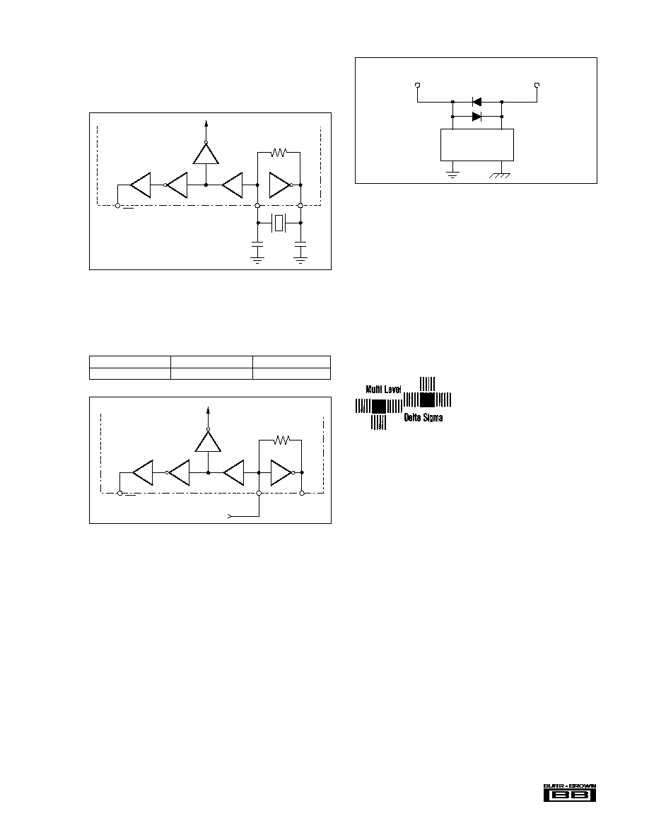
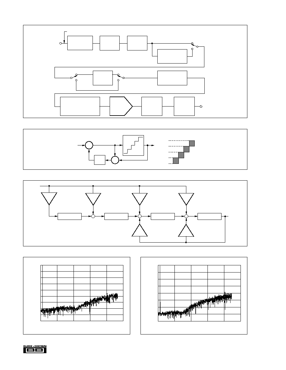
PCM1710 is an oversampling delta-sigma D/A converter,
consisting of an input interface/attenuator, a 4th-order multi-
level delta-sigma modulator, a low pass filter and an output
amplifier (see Figure 10).
Figure 8 is a diagram showing the internal clock with an
external clock source, instead of an oscillator. An exter-
nal system clock (input to XTI) must meet the follow-
ing conditions:
HIGH LEVEL
V
IH
> 0.64V
DD
T
H
> 10ns
LOW LEVEL
V
IH
> 0.28V
DD
T
L
> 10ns
FIGURE 8. External System Clock.
Internal System Clock
XTI
XTO
(1)
CLKO (XTI)
External System Clock Input
NOTE: (1) XTO must be open.
POWER SUPPLY CONNECTIONS
PCM1710 has two power supply connections: digital (V
DD
)
and analog (V
CC
). Each connection also has a separate
ground. If the power supplies turn on at different times, there
is a possibility of a latch-up condition. To avoid this condi-
tion, it is recommended to have a common connection
between the digital and analog power supplies. If separate
supplies are used without a common connection, the delta
between the two supplies during ramp-up time must be less
than 0.6V.
An application circuit to avoid a latch-up condition is shown
in Figure 9.
BYPASSING POWER SUPPLIES
The power supplies should be bypassed as close as possible
to the unit. Refer to Figure 19 for optimal values of bypass
capacitors. For applications which require very high perfor-
MODULATOR
The delta-sigma section of the PCM1710 is based on a 5-
level amplitude quantizer and a 4th-order filter. This con-
verts oversampled 16-or 20-bit input data to 5-level delta-
sigma format. A block diagram of the 5-level modulator is
shown in Figure 11.
This 5-level delta-sigma modulator has the advantage of
improved stability and jitter sensitivity over the typical one
bit (2-level) delta-sigma modulator.
The combined oversampling rate of the delta-sigma modula-
tor and the internal 8X oversampling digital filter is 48fs at
a system clock of 384fs and 32fs at a system clock of 256fs.
A block diagram of the 4th-order filter section Hf (z) in the
delta-sigma modulator is shown in Figure 12.
In general, high order one-bit delta-sigma modulators have
disadvantages due to loop instability (multiple integration
stages). The five level delta-sigma modulator of the PCM1710
uses phase compensation techniques to obtain stable opera-
tion. In Figure 12, the coefficients B1 to B4 give the basic
form of the filter, and A2 to A4 are used for phase compen-
sation of the feedback loop.
The theoretical quantization noise performance of five level
delta-sigma modulator is shown in Figure 13 and 14. In the
audio band, the quantization noise floor level of the PCM1710
is less than 130dB (at a system clock of 384fs).
DGND
AGND
V
DD
V
CC
Digital
Power Supply
Analog
Power Supply
Æ
PCM1710U
14
0
≠20
≠40
≠60
≠80
≠100
≠120
≠140
≠160
PCM1710 NOISE SHAPING AT 256fs
Frequency (kHz)
Gain (dB)
0
10
20
30
40
50
0
≠20
≠40
≠60
≠80
≠100
≠120
≠140
≠160
≠180
PCM1710 NOISE SHAPING AT 384fs
Frequency (kHz)
Gain (dB)
0
10
20
30
40
50
FIGURE 10. PCM1710 Block Diagram.
FIGURE 11. Block Diagram of Multi-level
Modulator.
FIGURE 12. Block Diagram of 4th-order Filter Section (H
f
(z)).
FIGURE 13. Theoretical Modulator Performance at 384fs.
FIGURE 14. Theoretical Modulator Performance at 256fs.
DAC
2nd-Order
LP Filter
CMOS
Amp
Interpolator
x6
De-emphasis
FIR-3
x2 T
TAP
FIR-1
x2 85
TAP
FIR-2
x2 15
TAP
4th-Order Multi-Level
Double Speed
Normal
8fs
Analog
Output
Vp-p = 3.2V
48fs (384fs System Clock)
Attenuator
Digital
Input
1fs (NM: Normal Mode)
2fs (DS: Double-Speed Dubbing Mode)
4fs (NM)
8fs (DS)
In
Out
+
+
4
3
2
1
0
Hf(Z)
5-level Quantizer
32fs/48fs
5-level
8fs
16/20-bits
Out
In
≠A1
B4
B3
B2
B1
≠A2
+
+
+
+
+
+
+
+
15
Æ
PCM1710U
1.0
0.5
0
≠0.5
≠1.0
dB
20
Frequency (Hz)
100
1k
10k
24k
SIMULATED ANALOG FILTER
FREQUENCY RESPONSE
(20Hz~24kHz, Expanded Scale)
APPLICATION
CONSIDERATIONS
16-BIT vs 20-BIT OPERATION
In the serial mode, PCM1710 can be configured to accept
either 16-bit or 20-bit data. The specifications listed in this
data sheet are the 16-bit data. Some improvements in
dynamic performance can be realized by using 20-bit data.
Internally, the PCM1710's digital filter uses only 20-bit
data. If the input data is 16-bit, the filter adds four zeros
to complete the 20-bit input word. Typical performance
differences between 16-bit and 20-bit data are shown in
Tables X and XI.
DATA
256fs
384fs
16-bit
≠91dB
≠93dB
20-bit
≠94dB
≠96dB
TABLE X. THD+N Performance at Full Scale.
DATA
256fs
384fs
16-bit
94dB
96dB
20-bit
96dB
98dB
TABLE XI. Dynamic Range.
DELAY TIME
There is a finite delay time in delta-sigma converters. In
A/D converters, this is commonly referred to as latency.
For a delta-sigma D/A converter, delay time is determined
by the order number of the FIR filter stage, and the chosen
sampling rate. The following equation expresses the delay
time of PCM1710:
T
D
= 22.625 x 1/fs
For f
S
= 44.1kHz, T
D
= 22.625/44.1kHz = 513.04
µ
s
Applications using data from a disc or tape source, such as
CD audio, CD-Interactive, Video CD, DAT, Minidisc, etc.,
generally are not affected by delay time. For some profes-
sional applications such as broadcast audio for studios, it is
important for total delay time to be less than 2ms.
INTERNAL RESET
If the sample rate clock (LRCIN) is stopped during opera-
tion, the infinite zero detect circuit will cause the output to
go to V
CC
/2 after 65,536 cycles of the bit clock (BCKIN).
Once a new system clock has been applied, there will be a
delay until output data is correlated to the input. This is
due to the digital delay of the filter.
When power is first applied to PCM1710, an automatic
reset function occurs after 64 cycles of LRCIN.
CHANGING SAMPLING RATE
For normal operation, LRCIN and XTI should be synchro-
nized at either 256fs or 384fs. When the sampling rate is
changed during operation, output data is invalid during the
delay period (T
D
) and for two subsequent cycles of LRCIN.
After two cycles of LRCIN, the output is a valid represen-
tation of the input data.
OUTPUT FILTERING
For testing purposes all dynamic tests are done on the
PCM1710 using a 20kHz low pass filter. This filter limits
the measured bandwidth for THD+N, etc. to 20kHz. Failure
to use such a filter will result in higher THD+N and lower
SNR and Dynamic Range readings than are found in the
specifications. The low pass filter removes out of band
noise. Although it is not audible, it may affect dynamic
specification numbers.
The performance of the internal low pass filter from DC to
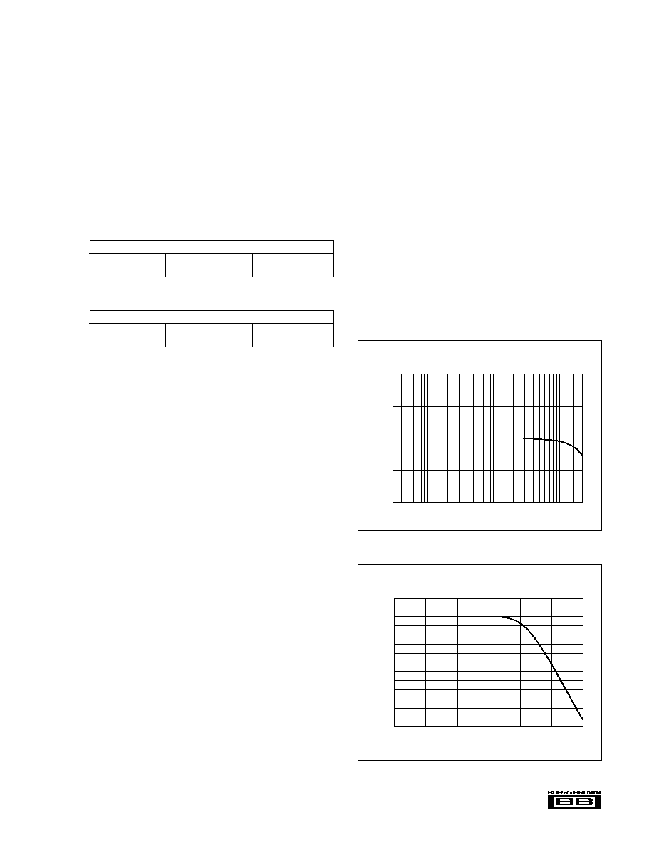
24kHz is shown in Figure 15. The higher frequency rolloff
of the filter is shown in Figure 16. If the user's application
has the PCM1710 driving a wideband amplifier, it is recom-
mended to use an external low pass filter. A simple 3rd-
order filter is shown in Figure 17. For some applications, a
passive RC filter or 2nd-order filter may be adequate.
FIGURE 15. Low Pass Filter Frequency Response.
FIGURE 16. Low Pass Filter Frequency Response.
10
5
0
≠5
≠10
≠15
≠20
≠25
≠30
≠35
≠40
≠45
≠50
≠55
10
100
1k
10k
100k
1M
10M
Frequency (Hz)
dB
≠60
SIMULATED ANALOG FILTER
FREQUENCY RESPONSE
(10Hz~10MHz)

Æ
PCM1710U
16
TEST CONDITIONS
Figure 18 illustrates the actual test conditions applied to
PCM1710 in production. The 11th-order filter is necessary
in the production environment for the removal of noise,
resulting from the relatively long physical distance between
the unit and the test analyzer. In most actual applications, the
third-order filter shown in Figure 17 is adequate. Under
normal conditions, THD+N typical performance is ≠70dB
with a 30kHz low pass filter (shown here on the THD
meter), improving to ≠92dB when the external 20kHz sec-
ond-order filter is used.
EVALUATION FIXTURES
Two different evaluation fixtures are available for PCM1710.
DEM-PCM1710
This evaluation fixture is primarily intended for quick evalu-
ation of the PCM1710's performance. DEM-PCM1710 can
accept either an external clock or a user-installed crystal
oscillator. All of the functions can be controlled by on-board
switches. DEM-PCM1710 does not contain a receiver chip
or an external low pass filter. DEM-PCM1710 requires a
single +5V power supply.
DEM-DAI1710
This fixture is more complete than DEM-PCM1710; it
includes a Digital Audio Interface (DAI) receiver chip for
easy use and to provide a low-jitter 256fs system clock to the
PCM1710. Also included are dual second-order low pass
filters using Burr-Brown's OPA2604 dual FET-input op
amp. The output of the DEM-DAI1710 is 2Vrms, using
standard BNC-type connectors.
All of the functions of PCM1710 can be evaluated by using
the DEM-DAI1710 jumper selections. DEM-DAI1710 re-
quires +5V and
±
5V to
±
15V power supplies. The schematic
diagram for DEM-DAI1710 is shown in Figure 19. For more
detailed information on the evaluation fixtures, contact your
local Burr-Brown representative.
FIGURE 17. 3rd-Order LPF.
10k
10k
10k
1500pF
100pF
680pF
+
V
SIN
≠
5
4
3
2
1
90
0
≠90
≠180
≠270
≠360
100
1k
10k
100k
1M
GAIN vs FREQUENCY
Frequency (Hz)
Phase (∞)
6
≠14
≠34
≠54
≠74
≠94
Gain (dB)
Gain
Phase
FIGURE 18. Test Block Diagram.
PGA
Digital
Lch
Rch
DEM-
DAI1710
CD
Player
11th-order
20kHz
LPF
THD
Meter
0dB/60dB
30KHz LPF on
Through
For test of S/N ratio and Dynamic Range, A-filter ON.
Test Disk
Shibasoku #725

17
Æ
PCM1710U
FIGURE 19. DEM-DAI1710 Schematic Circuit Diagram.
1
2
3
4
5
6
7
8
9
10
11
12
13
14
28
27
26
25
24
23
22
21
20
19
18
17
16
15
28
27
26
25
24
23
22
21
20
19
18
17
16
15
C
C
/FO
+V
D
DGND
RXP
RXN
FSYNC
SCK
CS12/FCK
SDATA
M1
+V
A
AGND
FRT
MCK
M3
C
5
0.1
µ
F
+
C
4
10
µ
F
C
2
0.047
µ
F
C
1
0.047
µ
F
C
7
10
µ
F
C
6
0.1
µ
F
C
3
0.047
µ
F
+
1
2
3
4
5
6
7
8
9
10
11
12
13
14
ML/DSD
MC/DM2
MD/DM1
MUTE
MODE
CKSL
DGND
V
DD
V
CC2L
AGND2L
EXT1L
EXT2L
V
OUTL
V
CC1
C
13
0.1
µ
F
C
12
10
µ
F
C
14
0.1
µ
F
C
15
10
µ
F
C
16
10
µ
F
C
27
100
µ
F
C
10
10
µ
F
+
+
+
+
+
+
+
+
+
C
8
10
µ
F
C
9
0.1
µ
F
C
11
10
µ
F
R
1
75
Digital In
R
4
10K
R
3
10K
R
15
10k
Q1
C1815 or
equivalent
+5V V
CC
+5V V
CC
U1
CS8412CP
U2
PCM1710U
J1
J2
J3
J4
R
2
1K
R
9
3.9k
R
11
100
R
7
10k
R
5
5.6k
C
17
4.7
µ
F
C
19
2700pF
C
24
0.1
µ
F
C
23
0.1
µ
F
C
21
330pF
Lch Out
+V
S
≠V
S
R
10
3.9k
R
12
100
R
8
10k
R
6
5.6k
C
18
4.7
µ
F
C
20
2700pF
C
22
330pF
1/2 U3
OPA2604
1/2 U3
OPA2604
Rch Out
GND
+V
CC
≠V
S
GND
+V
S
≠V
S
C
25
100
µ
F
R
13
10k
C
26
100
µ
F
R
14
10k
+5V V
CC
+V
S
CN
LRCIN
DIN
BCKIN
CLCKO
XTI
XTO
DGND
V
DD
V
CC2R
AGND2R
EXT1R
EXT2R
V
OUTR
AGND1