 | –≠–ª–µ–∫—Ç—Ä–æ–Ω–Ω—ã–π –∫–æ–º–ø–æ–Ω–µ–Ω—Ç: PCM1716 | –°–∫–∞—á–∞—Ç—å:  PDF PDF  ZIP ZIP |

Serial
Input
I/F
Mode
Control
I/F
8X Oversampling
Digital Filter with
Function
Controller
Crystal/OSC
XTI
SCK
XTO
CLKO
V
CC1
AGND1
V
DD
DGND
Enhanced
Multi-level
Delta-Sigma
Modulator
V
OUT
L
V
CC2
L
V
CC2
R
AGND2L
AGND2L
EXTL
Open Drain
DAC
Low-pass
Filter
Low-pass
Filter
BPZ-Cont.
V
OUT
R
EXTR
ZERO
DAC
MC/DM1
ML/IIS
LRCIN
DIN
BCKIN
CS/IWO
MD/DM0
MODE
MUTE
RST
Power Supply
24-Bit, 96kHz Sampling
CMOS Delta-Sigma Stereo Audio
DIGITAL-TO-ANALOG CONVERTER
49%
FPO
International Airport Industrial Park ∑ Mailing Address: PO Box 11400, Tucson, AZ 85734 ∑ Street Address: 6730 S. Tucson Blvd., Tucson, AZ 85706 ∑ Tel: (520) 746-1111 ∑ Twx: 910-952-1111
Internet: http://www.burr-brown.com/ ∑ FAXLine: (800) 548-6133 (US/Canada Only) ∑ Cable: BBRCORP ∑ Telex: 066-6491 ∑ FAX: (520) 889-1510 ∑ Immediate Product Info: (800) 548-6132
PCM1716
Æ
TM
DESCRIPTION
The PCM1716 is designed for Mid to High grade
Digital Audio applications which achieve 96kHz sam-
pling rates with 24-bit audio data. PCM1716 uses a
newly developed, enhanced multi-level delta-sigma
modulator architecture that improves audio dynamic
performance and reduces jitter sensitivity in actual
applications.
The internal digital filter operates at 8x over sampling
at a 96kHz sampling rate, with two kinds of roll-off
performances that can be selected: sharp roll-off, or
slow roll-off, as required for specific applications.
PCM1716 is suitable for Mid to High grade audio
applications such as CD, DVD-Audio, and Music
Instruments, since the device has superior audio
dynamic performance, 24-bit resolution and 96kHz
sampling.
FEATURES
q
ENHANCED MULTI-LEVEL DELTA-SIGMA DAC
q
SAMPLING FREQUENCY (f
s
): 16kHz - 96kHz
q
INPUT AUDIO DATA WORD:
16-, 20-, 24-Bit
q
HIGH PERFORMANCE:
THD+N: ≠96dB
Dynamic Range: 106dB
SNR: 106dB
Analog Output Range: 0.62 x V
CC
(Vp-p)
q
8x OVERSAMPLING DIGITAL FILTER:
Stop Band Attenuation: ≠82dB
Passband Ripple:
±
0.002dB
Slow Roll Off
q
MULTI FUNCTIONS:
Digital De-emphasis
L/R Independent Digital Attenuation
Soft Mute
Zero Detect Mute
Zero Flag
Chip Select
Reversible Output Phase
q
+5V SINGLE SUPPLY OPERATION
q
SMALL 28-LEAD SSOP PACKAGE
© 1997 Burr-Brown Corporation
PDS-1415C
Printed in U.S.A. August, 1998
PCM1716

Æ
2
PCM1716
SPECIFICATIONS
All specifications at +25
∞
C, +V
CC
= +V
DD
= +5V, f
S
= 44.1kHz, and 24-bit input data, SYSCLK = 384f
S
, unless otherwise noted.
PCM1716
PARAMETER
CONDITIONS
MIN
TYP
MAX
UNITS
RESOLUTION
24
Bits
DATA FORMAT
Audio Data Interface Format
Standard/I
2
S
Data Bit Length
16/20/24 Selectable
Audio Data Format
MSB First, 2's Comp
Sampling Frequency (f
S
)
16
96
kHz
System Clock Frequency
(1)
256/384/512/768f
S
DIGITAL INPUT/OUTPUT LOGIC LEVEL
Input Logic Level
V
IH
2.0
V
V
IL
0.8
V
Output Logic Level (CLKO) V
OH
I
OH
= 2mA
4.5
V
V
OL
I
OL
= 4mA
0.5
V
CLKO PERFORMANCE
(2)
Output Rise Time
20 ~ 80% V
DD
, 10pF
5.5
ns
Output Fall Time
80 ~ 20% V
DD
, 10pF
4
ns
Output Duty Cycle
10pF Load
37
%
DYNAMIC PERFORMANCE
(3)
(24-Bit Data)
THD+N
V
O
= 0dB
f
S
= 44.1kHz
≠97
≠90
dB
f
S
= 96kHz
≠94
dB
V
O
= ≠60dB
f
S
= 44.1kHz
≠42
dB
Dynamic Range
f
S
=44.1kHz EIAJ A-weighted
98
106
dB
f
S
= 96kHz A-weighted
103
dB
Signal-to-Noise Ratio
(4)
f
S
=44.1kHz EIAJ A-weighted
98
106
dB
f
S
= 96kHz A-weighted
103
dB
Channel Separation
f
S
= 44.1kHz
96
102
dB
f
S
= 96kHz
101
dB
DYNAMIC PERFORMANCE
(3)
(16-Bit Data)
THD+N
V
O
= 0dB
f
S
= 44.1kHz
≠94
dB
f
S
= 96kHz
≠92
dB
Dynamic Range
f
S
= 44.1kHz EIAJ A-weighted
98
dB
f
S
= 96kHz A-weighted
97
dB
DC ACCURACY
Gain Error
±
1.0
±
3.0
% of FSR
Gain Mismatch: Channel-to-Channel
±
1.0
±
3.0
% of FSR
Bipolar Zero Error
V
O
= 0.5V
CC
at Bipolar Zero
±
30
±
60
mV
ANALOG OUTPUT
Output Voltage
Full Scale (0dB)
0.62 V
CC
Vp-p
Center Voltage
0.5 V
CC
V
Load Impedance
AC Load
5
k
DIGITAL FILTER PERFORMANCE
Filter Characteristics 1
(Sharp Roll-Off)
Passband
±
0.002dB
0.454f
S
≠3dB
0.490f
S
Stopband
0.546f
S
Passband Ripple
±
0.002
dB
Stopband Attenuation
Stop Band = 0.546f
S
≠75
dB
Stop Band = 0.567f
S
≠82
dB
Filter Characteristics 2
(Slow Roll-Off)
Passband
±
0.002dB
0.274f
S
≠3dB
0.454f
S
Stopband
0.732f
S
Passband Ripple
±
0.002
dB
Stopband Attenuation
Stopband = 0.732f
S
≠82
dB
Delay Time
30/f
S
sec
De-emphasis Error
±
0.1
dB
INTERNAL ANALOG FILTER
≠3dB Bandwidth
100
kHz
Passband Response
f = 20kHz
≠0.16
dB
POWER SUPPLY REQUIREMENTS
Voltage Range
V
DD,
V
CC
4.5
5
5.5
VDC
Supply Current: I
CC
+I
DD
f
S
= 44.1kHz
32
45
mA
f
S
= 96kHz
45
mA
Power Dissipation
f
S
= 44.1kHz
160
225
mW
f
S
= 96kHz
225
mW
TEMPERATURE RANGE
Operation
≠25
+85
∞
C
Storage
≠55
+100
∞
C
NOTES: (1) Refer section of system clock. (2) External buffer is recommended. (3) Dynamic performance specs are tested with 20kHz low pass filter and THD+N
specs are tested with 30kHz LPF, 400Hz HPF, Average Mode. (4) SNR is tested at internally infinity zero detection off.

Æ
3
PCM1716
PIN
NAME
I/O
DESCRIPTION
1
LRCIN
IN
Left and Right Clock Input. This clock is equal to
the sampling rate - f
S
.
(1)
2
DIN
IN
Serial Audio Data Input
(1)
3
BCKIN
IN
Bit Clock Input for Serial Audio Data.
(1)
4
CLKO
OUT
Buffered Output of Oscillator. Equivalent to
System Clock.
5
XTI
IN
Oscillator Input (External Clock Input)
6
XTO
OUT
Oscillator Output
7
DGND
--
Digital Ground
8
V
DD
--
Digital Power +5V
9
V
CC
2R
--
Analog Power +5V
10
AGND2R
--
Analog Ground
11
EXTR
OUT
Rch, Common Pin of Analog Output Amp
12
NC
--
No Connection
13
V
OUT
R
OUT
Rch, Analog Voltage Output of Audio Signal
14
AGND1
--
Analog Ground
15
V
CC
1
--
Analog Power +5V
16
V
OUT
L
OUT
Lch, Analog Voltage Output of Audio Signal
17
NC
--
No Connection
18
EXTL
OUT
Lch, Common Pin of Analog Output Amp
19
AGND2L
--
Analog Ground
20
V
CC
2L
--
Analog Power +5V
21
ZERO
OUT
Zero Data Flag
22
RST
IN
Reset. When this pin is low, the DF and
modulators are held in reset.
(2)
23
CS/IWO
IN
Chip Select/Input Format Selection. When this
pin is low, the Mode Control is effective.
(3)
24
MODE
IN
Mode Control Select. (H: Software, L: Hardware)
(2)
25
MUTE
IN
Mute Control
26
MD/DM0
IN
Mode Control, DATA/De-emphasis Selection 1
(2)
27
MC/DM1
IN
Mode Control, BCK/De-emphasis Selection 2
(2)
28
ML/I
2
S
IN
Mode Control, WDCK/Input Format Selection
(2)
NOTES: (1) Pins 1, 2, 3; Schmitt Trigger input. (2) Pins 22, 24, 25, 26, 27,
28; Schmitt Trigger input with pull-up resister. (3) Pin 23; Schmitt Trigger
input with pull-down resister.
PIN ASSIGNMENTS
PIN CONFIGURATION
LRCIN
DIN
BCKIN
CLKO
XTI
XTO
DGND
V
DD
V
CC
2R
AGND2R
EXTR
NC
V
OUT
R
AGND1
ML/IIS
MC/DM1
MD/DM0
MUTE
MODE
CS/IWO
RST
ZERO
V
CC
2L
AGND2L
EXTL
NC
V
OUT
L
V
CC
1
1
2
3
4
5
6
7
8
9
10
11
12
13
14
28
27
26
25
24
23
22
21
20
19
18
17
16
15
PCM1716E
PACKAGE DRAWING
PRODUCT
PACKAGE
NUMBER
(1)
PCM1716E
28-Pin SSOP
324
NOTE: (1) For detailed drawing and dimension table, please see end of data
sheet, or Appendix C of Burr-Brown IC Data Book.
PACKAGE INFORMATION
ELECTROSTATIC
DISCHARGE SENSITIVITY
This integrated circuit can be damaged by ESD. Burr-Brown
recommends that all integrated circuits be handled with
appropriate precautions. Failure to observe proper handling
and installation procedures can cause damage.
ESD damage can range from subtle performance degradation
to complete device failure. Precision integrated circuits may
be more susceptible to damage because very small parametric
changes could cause the device not to meet its published
specifications.
Power Supply Voltage ...................................................................... +6.5V
+V
CC
to +V
DD
Difference ...................................................................
±
0.1V
Input Logic Voltage .................................................. ≠0.3V to (V
DD
+ 0.3V)
Input Current (except power supply) ...............................................
±
10mA
Power Dissipation .......................................................................... 400mW
Operating Temperature Range ......................................... ≠25
∞
C to +85
∞
C
Storage Temperature ...................................................... ≠55
∞
C to +125
∞
C
Lead Temperature (soldering, 5s) ................................................. +260
∞
C
ABSOLUTE MAXIMUM RATINGS
The information provided herein is believed to be reliable; however, BURR-BROWN assumes no responsibility for inaccuracies or omissions. BURR-BROWN assumes
no responsibility for the use of this information, and all use of such information shall be entirely at the user's own risk. Prices and specifications are subject to change
without notice. No patent rights or licenses to any of the circuits described herein are implied or granted to any third party. BURR-BROWN does not authorize or warrant
any BURR-BROWN product for use in life support devices and/or systems.
Æ
4
PCM1716
≠60dB OUTPUT SPECTRUM
(f = 1kHz, f
S
= 44.1kHz, 24-Bit Data)
Frequency (Hz)
Amplitude (dB)
≠60
≠70
≠80
≠90
≠100
≠110
≠120
≠130
≠140
≠150
20
2
4
6
8
10
12
14
16
18
20
≠60dB OUTPUT SPECTRUM
(f = 1kHz, f
S
= 44.1kHz, 16-Bit Data)
Frequency (Hz)
Amplitude (dB)
≠60
≠70
≠80
≠90
≠100
≠110
≠120
≠130
≠140
≠150
20
2
4
6
8
10
12
14
16
18
20
TYPICAL PERFORMANCE CURVES
All specifications at +25
∞
C, +V
CC
= +V
DD
= +5V, f
S
= 44.1kHz, and 24-bit input data, SYSCLK = 384f
S
, unless otherwise noted.
THD+N vs SAMPLING FREQUENCY
(V
CC
= V
DD
= 5V, 24-Bit)
Sampling Frequency f
S
(kHz)
THD+N at F/S (dB)
88
91
94
97
100
103
32
44.1
48
96
256fs
384fs
DYNAMIC RANGE vs SAMPLING FREQUENCY
(V
CC
= V
DD
= 5V, 24-Bit)
Sampling Frequency f
S
(kHz)
Dynamic Range (A-weighted) (dB)
110
108
106
104
102
100
32
44.1
48
96
256/384f
S
THD+N vs LEVEL
(f
S
= 44.1kHz)
Amplitude (dB)
THD+N (%)
10
1
0.1
0.010
0.001
THD+N (dB)
≠20
≠40
≠60
≠80
≠100
≠30
≠50
≠70
≠90
≠50
≠60
≠40
≠30
≠20
≠10
0
16-Bit
24-Bit
SNR vs SAMPLING FREQUENCY
(V
CC
= V
DD
= 5V, 24-Bit)
Sampling Frequency f
S
(kHz)
SNR (A-weighted) (dB)
110
108
106
104
102
100
32
44.1
48
96
256/384f
S

Æ
5
PCM1716
0
0.5
1.5
1
2.5
2
3.5
3
4
0
≠20
≠40
≠60
≠80
≠100
≠120
≠140
Amplitude (dB)
OVERALL FREQUENCY CHARACTERISTIC
(Slow Roll-Off)
Frequency (x f
S
)
0
0.5
1
1.5
2
2.5
3
3.5
4
0
≠20
≠40
≠60
≠80
≠100
≠120
≠140
≠160
Amplitude (dB)
OVERALL FREQUENCY CHARACTERISTIC
(Sharp Roll-Off)
Frequency (x f
S
)
TYPICAL PERFORMANCE CURVES
(CONT)
0
0.1
0.2
0.3
0.4
0.5
0.6
0
≠2
≠4
≠6
≠8
≠10
≠12
≠14
≠16
≠18
≠20
Amplitude (dB)
FREQUENCY CHARACTERISTIC
(Slow Roll-Off)
Frequency (x f
S
)
0
0.1
0.2
0.3
0.4
0.5
0.003
0.002
0.001
0
≠0.001
≠0.002
≠0.003
Amplitude (dB)
PASSBAND RIPPLE CHARACTERISTIC
(Sharp Roll-Off)
Frequency (x f
S
)
DE-EMPHASIS FREQUENCY RESPONSE (f
S
= 32kHz)
0
2
4
6
8
10
12
14
Frequency (kHz)
0
≠2
≠4
≠6
≠8
≠10
Level (dB)
DE-EMPHASIS FREQUENCY RESPONSE (f
S
= 48kHz)
0
2
4
6
8
10
12
14
16
18
20
22
Frequency (kHz)
0
≠2
≠4
≠6
≠8
≠10
Level (dB)
DE-EMPHASIS FREQUENCY RESPONSE (f
S
= 44.1kHz)
0
2
4
6
8
10
12
14
16
18
20
Frequency (kHz)
0
≠2
≠4
≠6
≠8
≠10
Level (dB)
DE-EMPHASIS ERROR (f
S
= 32kHz)
0
2
4
6
8
10
12
14
Frequency (kHz)
0.5
0.3
0.1
≠0.1
≠0.3
≠0.5
0.5
0.3
0.1
≠0.1
≠0.3
≠0.5
0.5
0.3
0.1
≠0.1
≠0.3
≠0.5
Level (dB)
DE-EMPHASIS ERR0R (f
S
= 48kHz)
0
2
4
6
8
10
12
14
16
18
20
22
Frequency (kHz)
Level (dB)
DE-EMPHASIS ERROR (f
S
= 44.1kHz)
0
2
4
6
8
10
12
14
16
18
20
Frequency (kHz)
Level (dB)
Æ
6
PCM1716
SYSTEM CLOCK
The system clock for PCM1716 must be either 256f
S
, 384f
S
,
512f
S
or 768f
S
, where f
S
is the audio sampling frequency
(typically 32kHz, 44.1kHz, 48kHz, or 96kHz). But 768f
S
at
96kHz is not accepted.
The system clock can be either a crystal oscillator placed
between XTI (pin 5) and XTO (pin 6), or an external clock
input to XTI. If an external system clock is used, XTO is
open (floating). Figure 1 illustrates the typical system clock
connections.
PCM1716 has a system clock detection circuit which auto-
matically senses if the system clock is operating at 256f
S
~
768f
S
. The system clock should be synchronized with LRCIN
(pin 1) clock. LRCIN (left-right clock) operates at the sam-
pling frequency f
S
. In the event these clocks are not synchro-
nized, PCM1716 can compensate for the phase difference
internally. If the phase difference between left-right and
system clocks is greater than 6-bit clocks (BCKIN), the
synchronization is performed internally. While the synchro-
nization is processing, the analog output is forced to a DC
level at bipolar zero. The synchronization typically occurs in
less than 1 cycle of LRCIN.
SYSTEM CLOCK FREQUENCY - MHz
SAMPLING RATE FREQUENCY (f
S
) - LRCIN
256f
S
384f
S
512f
S
768f
S
32kHz
8.1920
12.2880
16.3840
24.5760
44.1kHz
11.2896
16.9340
22.5792
33.8688
(1)
48kHz
12.2880
18.4320
24.5760
36.8640
(1)
96kHz
24.5760
36.8640
(1)
49.1520
(1)
--
NOTE: (1) The Internal Crystal oscillator frequency cannot be larger than 24.576MHz.
TABLE I. Typical System Clock Frequency.
Typical input system clock frequencies to the PCM1716 are
shown in Table I, also, external input clock timing require-
ments are shown in Figure 2.
FIGURE 1. System Clock Connection.
FIGURE 2. XTI Clock Timing.
t
SCKH
System Clock Pulse Width High t
SCKIH
: 7ns MIN
System Clock Pulse Width Low t
SCKIL
: 7ns MIN
t
SCKL
2.0V
0.8V
"H"
"L"
XTI
DATA INTERFACE FORMATS
Digital audio data is interfaced to PCM1716 on pins 1, 2,
and 3, LRCIN (left-right clock), DIN (data input) and
BCKIN (bit clock). PCM1716 can accept both standard, I
2
S,
and left justified data formats.
Figure 3 illustrates acceptable input data formats. Figure 4
shows required timing specification for digital audio data.
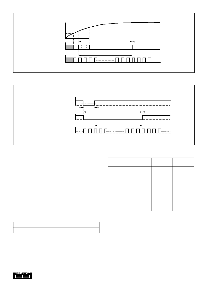
Reset
PCM1716 has both internal power-on reset circuit and the
RST pin (pin 22) which accepts an external forced reset by
RST = LOW. For internal power on reset, initialize (reset) is
done automatically at power on V
DD
>2.2V (typ). During
internal reset = LOW, the output of the DAC is invalid and
the analog outputs are forced to V
CC
/2. Figure 5 illustrates
the timing of the internal power on reset.
PCM1716 accepts an external forced reset when RST = L.
When RST = L, the output of the DAC is invalid and the
analog outputs are forced to V
CC
/2 after internal initialization
(1024 system clocks count after RST = H.) Figure 6 illustrates
the timing of the RST pin.
Zero Out (pin 21)
If the input data is continuously zero for 65536 cycles of
BCK, an internal FET is switched to "ON". The drain of the
internal FET is the zero-pin, it will enable "wired-or" with
external circuit. This zero detect function is available in both
software mode and hardware mode.
System Clock
(256/384/
512/768f
S
)
Externl Clock Input
CLKO
XTI
XTO
4
5
6
PCM1716
System Clock
Buffer Out
Crystal Resonator Oscillation
CLKO
XTI
XTO
4
5
6
PCM1716
XTAL
C
1
C
2
C
1
C
2
: 10pF ~ 30pF
Buffer

Æ
7
PCM1716
14
15
16
1
2
3
14
15
1/f
S
L_ch
R_ch
MSB
LSB
16
LRCIN (pin 1)
BCKIN (pin 3)
(1) 16-Bit Right Justified
DIN (pin 2)
1
2
3
14
15
MSB
LSB
16
18
19
20
1
2
3
18
19
MSB
LSB
20
(2) 20-Bit Right Justified
DIN (pin 2)
1
2
3
18
19
MSB
LSB
20
23
24
1
2
3
22
23
MSB
LSB
24
(3) 24-Bit Right Justified
DIN (pin 2)
(4) 24-Bit Left Justified
DIN (pin 2)
1
2
3
22
23
MSB
LSB
24
1
2
3
22
23
MSB
LSB
24
1
2
3
22
23
MSB
LSB
24
1
2
3
14
15
1/f
S
L_ch
R_ch
MSB
LSB
16
LRCIN (pin 1)
BCKIN (pin 3)
(5) 16-Bit I
2
S
DIN (pin 2)
1
2
3
14
15
MSB
LSB
16
2
1
2
1
1
2
3
22
23
MSB
LSB
24
(6) 24-Bit I
2
S
DIN (pin 2)
1
2
3
22
23
MSB
LSB
24
FIGURE 3. Audio Data Input Formats.
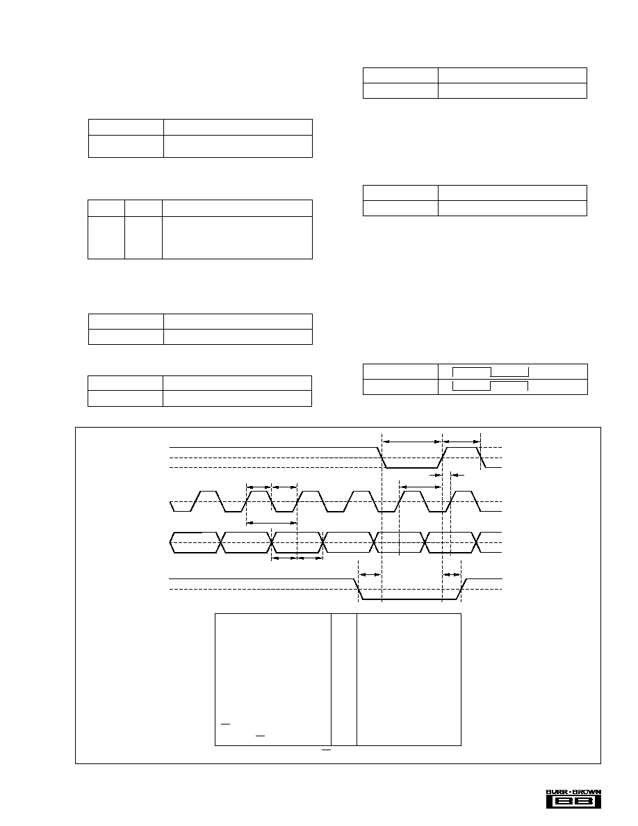
LRCKIN
BCKIN
DIN
1.4V
1.4V
1.4V
t
BCH
t
BCL
t
LB
t
BL
t
DS
BCKIN Pulse Cycle Time
BCKIN Pulse Width High
BCKIN Pulse Width Low
BCKIN Rising Edge to LRCIN Edge
LRCIN Edge to BCKIN Rising Edge
DIN Set-up Time
DIN Hold Time
: t
BCY
: t
BCH
: t
BCL
: t
BL
: t
LB
: t
DS
: t
DH
: 100ns (min)
: 50ns (min)
: 50ns (min)
: 30ns (min)
: 30ns (min)
: 30ns (min)
: 30ns (min)
t
DH
t
BCY
FIGURE 4. Audio Data Input Timing Specification.
Æ
8
PCM1716
1024 system (XTI) clocks
Reset
Reset Removal
XTI Clock
Internal Reset
RST
t
RST
(1)
NOTE: (1) t
RST
= 20ns min.
1024 system (= XTI) clocks
Reset
Reset Removal
V
CC
= V
DD
Internal Reset
XTI Clock
FIGURE 5. Internal Power-On Reset Timing.
FUNCTIONAL DESCRIPTION
PCM1716 has several built-in functions including digital
attenuation, digital de-emphasis, input data format selection,
and others. These functions are software controlled. PCM1716
can be operated in two different modes, software mode or
hardware mode. Software mode is a three-wire interface
using pin 28 (ML), 27 (MC), and 26 (MD).
PCM1716 can also be operated in hardware mode, where
static control signals are used on pin 28 (115, pin 27 (DM1),
pin 26 (DM0) and pin 23 (IWO).
This basic operation mode as software or hardware can be
selected by pin 24 (MODE) as shown in Table II.
MODE (pin 24) = H
Software Mode
MODE (pin 24) = L
Hardware Mode
TABLE II. Mode Control.
Table III indicates which functions are selectable within the
users chosen mode. All of the functions shown are selectable
within the software mode, but only de-emphasis control, soft
mute and input data format may be selected when using
PCM1716 in the hardware mode.
SOFTWARE
HARDWARE
FUNCTION
(Mode = H)
(Mode = L)
Input Data Format Selection
O
O
Input Data Bit Selection
O
O
Input LRCIN Polarity Selection
O
X
De-emphasis Control
O
O
Mute
O
O
Attenuation
O
X
Infinity Zero Mute Control
O
X
DAC Operation Control
O
X
Slow Roll-Off Selection
O
X
Output Phase Selection
O
X
CLKO Output Selection
O
X
NOTE: O = Selectable, X: Not Selectable.
TABLE III. Mode Control, Selectable Functions.
HARDWARE MODE (MODE = L)
In hardware mode, the following function can be selected.
De-emphasis control
De-emphasis control can be selected by DM1 (pin 27) and
DM0 (pin 26)
FIGURE 6. External Forced Reset Timing.
Æ
9
PCM1716
Input Audio Data Format
Input data format can be selected by I
2
S (pin 28) and IWO
(pin 23)
DM1 (Pin 27)
DM0 (Pin 26)
DE-EMPHASIS
L
L
OFF
L
H
48kHz
H
L
44.1kHz
H
H
32kHz
TABLE IV. De-emphasis Control.
I
2
S (Pin 28)
IWO (Pin 23)
DATA FORMAT
L
L
16-Bit Data Word, Normal, Right Justified
L
H
20-Bit Data Word, Normal, Right Justified
H
L
16-Bit Data Word, I
2
S Format
H
H
24-Bit Data Word, I
2
S Format
TABLE V. Data Format Control.
SOFT MUTE
Soft Mute function can be controlled by MUTE (pin 25)
SOFTWARE MODE (MODE = H)
PCM1716's special functions at software mode is shown in
Table VI. These functions are controlled using a ML, MC,
MD serial control signal.
MUTE (Pin 25)
SOFT MUTE
L
Mute ON
H
Mute OFF (Normal Operation)
FUNCTION
DEFAULT MODE
Input Audio Data Format Selection
Standard Format
Left Justified
Standard Format
I
2
S Format
Input Audio Data Bit Selection
16-Bit
16-Bit
20-Bit
24-Bit
Input LRCIN Polarity Selection
Lch/Rch = High/Low
Lch/Rch = High/Low
Lch/Rch = Low/High
De-emphasis Control
OFF
Soft Mute Control
OFF
Attenuation Control
Lch, Rch Individually
0dB, Individual
Lch, Rch Common
Infinite Zero Mute Control
Not Operated
DAC Operation Control
Operated
Sampling Rate Selection for De-emphasis
Standard Frequency
44.1kHz
44.1kHz
48kHz
32kHz
Slow Roll-Off Selection
Not Selected
(Sharp Roll-Off)
Output Phase Selection
Not Inverted
CLK0 Output Selection
Input Frequency
TABLE VI. Selectable Functions and Default.
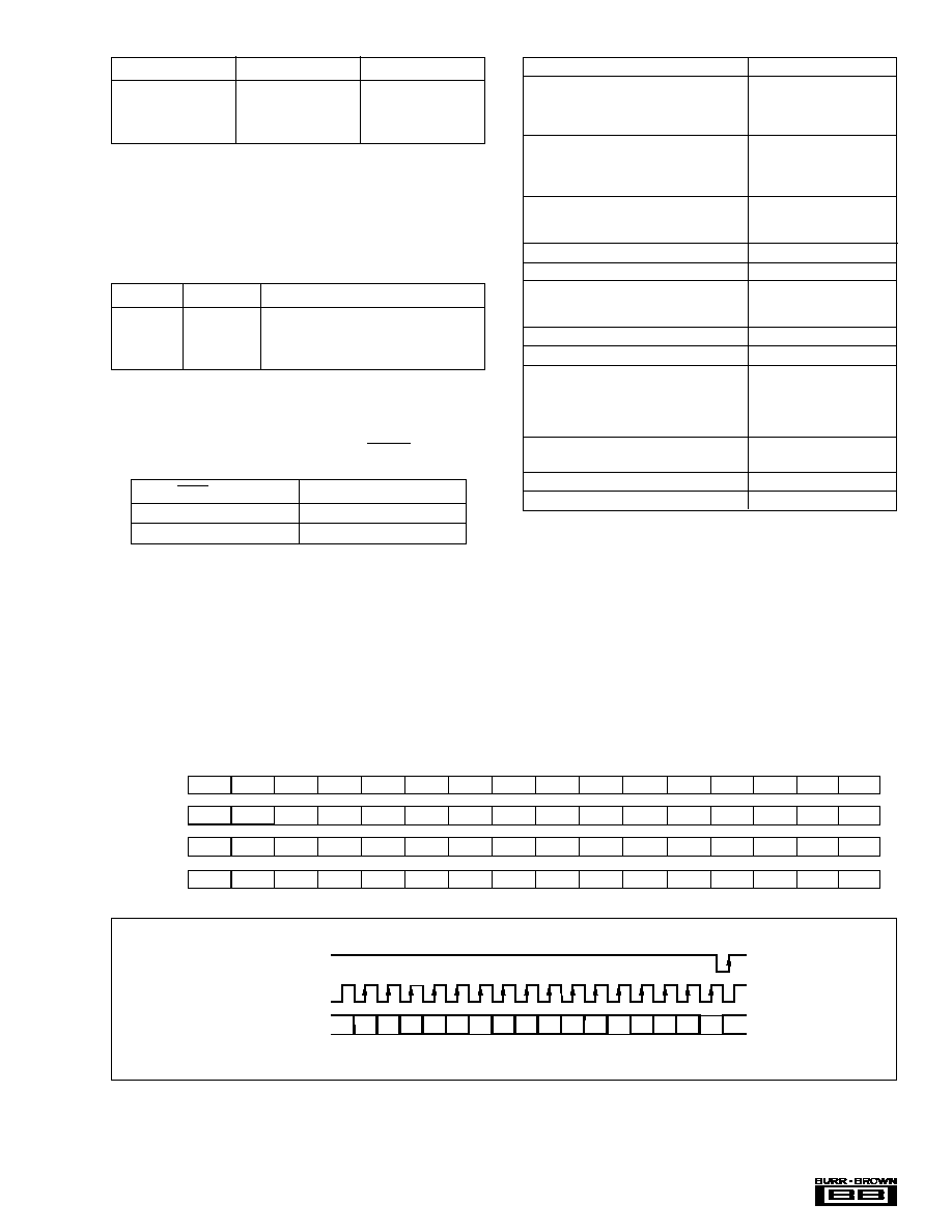
PROGRAM REGISTER BIT MAPPING
PCM1716's special functions are controlled using four pro-
gram registers which are 16 bits long. These registers are all
loaded using MD. After the 16 data bits are clocked in, ML
is used to latch in the data to the appropriate register. Table
VII shows the complete mapping of the four registers and
Figure 7 illustrates the serial interface timing.
MAPPING OF PROGRAM REGISTERS
B15
B14
B13
B12
B11
B10
B9
B8
B7
B6
B5
B4
B3
B2
B1
B0
MODE0
res
res
res
res
res
A1
A0
LDL
AL7
AL6
AL5
AL4
AL3
AL2
AL1
AL0
MODE1
res
res
res
res
res
A1
A0
LDR
AR7
AR6
AR5
AR4
AR3
AR2
AR1
AR0
MODE2
res
res
res
res
res
A1
A0
res
res
res
res
IW1
IW0
OPE
DEM
MUT
MODE3
res
res
res
res
res
A1
A0
IZD
SF1
SF0
CK0
REV
SR0
ATC
LRP
I
2
S
FIGURE 7. Three-Wire Serial Interface.
B15 B14 B13 B12 B11 B10 B9 B8 B7 B6 B5 B4 B3 B2 B1 B0
ML (pin 28)
MC (pin 27)
MD (pin 26)

Æ
10
PCM1716
REGISTER
BIT
NAME
NAME
DESCRIPTION
Register 0
AL (7:0)
DAC Attenuation Data for Lch
LDL
Attenuation Data Load Control for Lch
A (1:0)
Register Address
res
Reserved, should be "L"
Register 1
AR (7:0)
DAC Attenuation Data for Rch
LDR
Attenuation Data Load Control for Rch
A (1:0)
Register Address
res
Reserved, should be "L"
Register 2
MUT
Left and Right DACs Soft Mute Control
DEM
De-emphasis Control
OPE
Left and Right DACs Operation Control
IW (1:0)
Input Audio Data Bit and Format Select
res
Reserved
A (1:0)
Register Address
res
Reserved, should be "L"
Register 3
I
2
S
Audio Data Format Select
LRP
Polarity of LRCIN Select
ATC
Attenuator Control
SRO
Slow Roll-Off Select
REV
Output Phase Select
CKO
CLKO Output Select
SF (1:0)
Sampling Rate Select
IZD
Internal Zero Detection Circuit Control
A (1:0)
Register Address
res
Reserved, should be "L"
TABLE VII. Register Functions
REGISTER 0 (A1 = 0, A0 = 0)
B15 B14 B13 B12 B11 B10 B9 B8
B7 B6
B5
B4 B3
B2
B1 B0
res res res res res A1 A0 LDL AL7 AL6 AL5 AL4 AL3 AL2 AL1 AL0
Register 0 is used to control left channel attenuation. Bits
0 - 7 (AL0 - AL7) are used to determine the attenuation
level. The level of attenuation is given by:
ATT = 0.5 x (data-255) (dB)
FFh = ≠0dB
FEh = ≠0.5dB
:
:
01h = ≠127.5dB
00h = ≠
(= Mute)
ATTENUATION DATA LOAD CONTROL
Bit 8 (LDL) is used to control the loading of attenuation data
in B0:B7. When LDL is set to 0, attenuation data will be
loaded into AL0:AL7, but it will not affect the attenuation
level until LDL is set to 1. LDR in Register 1 has the same
function for right channel attenuation.
REGISTER 1 (A1 = 0, A0 = 1)
B15 B14 B13 B12 B11 B10 B9 B8
B7 B6
B5
B4 B3
B2
B1 B0
res res res res res A1 A0 LDR AR7 AR6 AR5 AR4 AR3 AR2 AR1 AR0
Register 1 is used to control right channel attenuation. As
in Register 1, bits 0 - 7 (AR0 - AR7) control the level of
attenuation.
Register 2 is used to control soft mute, de-emphasis, opera-
tion enable, input resolution, and input audio data bit and
format.
REGISTER 2 (A1 = 1, A0 = 0)
B15 B14 B13 B12 B11 B10 B9 B8
B7 B6
B5
B4 B3
B2
B1
B0
res res res res res A1 A0 res
res res res IW1 IWO OPE DEM MUTE
when OPE (B2) is "HIGH", the output of the DAC will be
forced to bipolar zero, irrespective of any input data.
IWO (B3), IW1 (B4) and I
2
S (B0) of Register 3
These resisters, IWO, IW1, I
2
S determine the input data
word and input data format as shown below.
IW1
IW0
I
2
S
Audio Interface
0
0
0
16-Bit Standard (Right-Justified)
0
1
0
20-Bit Standard (Right-Justified)
1
0
0
24-Bit Standard (Right-Justified)
1
1
0
24-Bit Left-Justified (MSB First)
0
0
1
16-Bit I
2
S
0
1
1
24-Bit I
2
S
1
0
1
Reserved
1
1
1
Reserved
REGISTER 3 (A1 = 1, A0 = 1)
B15 B14 B13 B12 B11 B10 B9 B8
B7 B6
B5
B4 B3
B2
B1
B0
res res res res res A1 A0 IZD
SF1 SF0 CKO REV SRO ATC LRP I
2
S
REGISTER 3 (A1 = 1, A0 = 1)
Register 3 is used to control input data format and polarity,
attenuation channel control, system clock frequency, sam-
pling frequency, infinite zero detection, output phase,
CLKO output, and slow roll-off.
Bit 8 is used to control the infinite zero detection function
(IZD).
When IZD is "LOW", the zero detect circuit is off. Under
this condition, no automatic muting will occur if the input
is continuously zero. When IZD is "HIGH", the zero detect
feature is enabled. If the input data is continuously zero for
65, 536 cycles of BCKIN, the output will be immediately
MUT (B0)
MUT = L
Soft Mute OFF
MUT = H
Soft Mute ON
OPE (B2)
OPE = L
Normal Operation
OPE = H
DAC Operation OFF
DEM (B1)
DEM = L
De-emphasis OFF
DEM = H
De-emphasis ON
Æ
11
PCM1716
forced to a bipolar zero state (V
CC
/ 2). The zero detection
feature is used to avoid noise which may occur when the
input is DC. When the output is forced to bipolar zero,
there may be an audible click. PCM1716 allows the zero
detect feature to be disabled so the user can implement an
external muting circuit.
SRO (B3) is roll-off performance of digital filter selection.
SRO = L
Sharp Roll-Off
SRO = H
Slow Roll-Off
ATC (B2) is used as an attenuation control. When bit 3 is
set HIGH, the attenuation data on Register 0 is used for
both channels, and the data in Register 1 is ignored. When
bit 3 is LOW, each channel has separate attenuation data.
ATC = L
Ch Individual ATT Control
ATC = H
Common ATT Control
Bits 0 (I
2
S) and 1 (LRP) are used to control the input data
format. A "LOW" on bit 0 sets the format to (MSB-first,
right-justified Japanese format) and a "HIGH" sets the
format to I
2
S (Philips serial data protocol). Bit 1 (LRP) is
used to select the polarity of LRCIN (sample rate clock).
When bit 1 is "LOW", left channel data is assumed when
LRCIN is in a "HIGH" phase and right channel data is
assumed when LRCIN is in a "LOW" phase. When bit 1 is
"HIGH", the polarity assumption is reversed.
LRP = L
L
R
H/Lch
LRP = H
L
R
L/Lch
FIGURE 8. Program Register Input Timing.
IZD (B8)
B8 = L
Zero Detect Mute OFF
B8 = H
Zero Detect Mute ON
Bits 6 (SF0) and 7 (SF1) are used to select the sampling
frequency for De-emphasis.
SF1
SF0
Sampling Rate
0
0
Reserved
0
1
48kHz
1
0
44.1kHz
1
1
32kHz
CKO (B5) is output frequency control at CLKO pin, can be
selected as Buffer (1/1) or half rate of input frequency
(1/2).
CKO = L
Buffer Out of XTi Clock
CKO = H
Half (1/2) Frequency Out of XTi Clock
REF (B4) is output analog signal phase control.
REV = L
Normal Output
REV = H
Inverted Output
1.4V
1.4V
1.4V
ML
MC
MD
t
MLH
t
MCH
t
MCL
t
MDS
t
MCY
t
MLS
t
MLL
t
MHH
1.4V
CS
t
CSML
t
MLCS
t
MDH
LSB
MC Pulse Cycle Time
MC Pulse Width LOW
MC Pulse Width HIGH
MD Hold Time
MD Set-up Time
ML Low Level Time
ML High Level Time
ML Hold Time
ML Set-up Time
CS Low to ML Low Time
(2)
ML High to CS High Time
(2)
NOTE: (1) System Clock Cycle. (2) CS Should be changed during ML = H.
: t
MCY
: t
MCL
: t
MCH
: t
MDH
: t
MDS
: t
MLL
: t
MHH
: t
MLH
: t
MLS
: t
CSML
: t
MLCS
: 100ns (min)
: 40ns (min)
: 40ns (min)
: 40ns (min)
: 40ns (min)
: 40ns (min) + 1SYSCLK
(1)
(min)
: 40ns (min) + 1SYSCLK
(1)
(min)
: 40ns (min)
: 40ns (min)
: 10ns (min)
: 10ns (min)

Æ
12
PCM1716
THEORY OF OPERATION
The delta-sigma section of PCM1716 is based on a 8-level
amplitude quantizer and a 4th-order noise shaper. This
section converts the oversampled input data to 8-level delta-
sigma format.
This newly developed, "Enhanced Multi-level Delta-Sigma"
architecture achieves high-grade audio dynamic performance
and sound quality.
A block diagram of the 8-level delta-sigma modulator is
shown in Figure 9. This 8-level delta-sigma modulator has
the advantage of stability and clock jitter sensitivity over the
typical one-bit (2 level) delta-sigma modulator.
The combined oversampling rate of the delta-sigma modu-
lator and the internal 8-times interpolation filter is 64f
S
for
all system clock ratios (256/384/512/768f
S
).
The theoretical quantization noise performance of the
8-level delta-sigma modulator is shown in Figure 10. This
enhanced multi-level delta-sigma architecture also has ad-
vantages for input clock jitter sensitivity due to the multi-
level quantizer, simulated jitter sensitivity is shown in
Figure 11.
+
Z
≠1
8-Level Quantizer
+
Z
≠1
+
Z
≠1
≠
+
Z
≠1
+
+
FIGURE 9. 8-Level Delta-Sigma Modulator.
0
1
2
3
4
5
6
7
8
0
≠20
≠40
≠60
≠80
≠100
≠120
≠140
≠160
≠180
Amplitude (dB)
Frequency (f
S
)
FIGURE 10. Quantization Noise Spectrum.
FIGURE 11. Jitter Sensitivity.
0
100
200
300
400
500
600
125
120
115
110
105
100
95
90
85
80
Dynamic Range (dB)
Jitter (ps)
CLOCK JITTER

Æ
13
PCM1716
APPLICATION
CONSIDERATIONS
DELAY TIME
There is a finite delay time in delta-sigma converters. In A/D
converters, this is commonly referred to as latency. For a
delta-sigma D/A converter, delay time is determined by the
order number of the FIR filter stage, and the chosen sampling
rate. The following equation expresses the delay time of
PCM1716:
T
D
= 30
x
1/f
S
For f
S
= 44.1kHz, T
D
= 30/44.1kHz = 680
µ
s
Applications using data from a disc or tape source, such as
CD audio, DVD audio, Video CD, DAT, Minidisc, etc.,
generally are not affected by delay time. For some profes-
sional applications such as broadcast audio for studios, it is
important for total delay time to be less than 2ms.
OUTPUT FILTERING
For testing purposes all dynamic tests are done on the
PCM1716 using a 20kHz low pass filter. This filter limits
the measured bandwidth for THD+N, etc. to 20kHz. Failure
to use such a filter will result in higher THD+N and lower
SNR and Dynamic Range readings than are found in the
specifications. The low pass filter removes out of band
noise. Although it is not audible, it may affect dynamic
specification numbers.
The performance of the internal low pass filter from DC to
40kHz is shown in Figure 12. The higher frequency roll-off
of the filter is shown in Figure 13. If the user's application
has the PCM1716 driving a wideband amplifier, it is recom-
mended to use an external low pass filter.
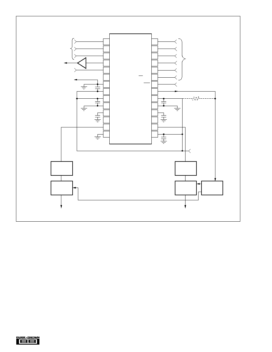
BYPASSING POWER SUPPLIES
The power supplies should be bypassed as close as possible
to the unit. Refer to Figure 15 for optimal values of bypass
capacitors.
POWER SUPPLY
CONNECTIONS
PCM1716 has three power supply connections: digital (V
DD
),
and analog (V
CC
). Each connection also has a separate
ground. If the power supplies turn on at different times, there
is a possibility of a latch-up condition. To avoid this condi-
tion, it is recommended to have a common connection
between the digital and analog power supplies. If separate
supplies are used without a common connection, the delta
between the two supplies during ramp-up time must be less
than 0.1V.
An application circuit to avoid a latch-up condition is shown
in Figure 14.
FIGURE 12. Low Pass Filter Response.
1
10
100
1k
10k
100k
1
0.5
0
≠0.5
≠1
Level (dB)
Log Frequency (Hz)
FIGURE 13. Low Pass Filter Response.
1
10
100
1k
10k
100k
1M
10M
20
0
≠20
≠40
≠60
≠80
≠100
Level (dB)
Log Frequency (Hz)
FIGURE 14. Latch-Up Prevention Circuit.
DGND
AGND
V
DD
V
CC
Digital
Power Supply
Analog
Power Supply
Æ
14
PCM1716
1
2
3
4
5
6
7
8
9
10
11
12
13
14
LRCIN
DIN
BCKIN
CLKO
XTI
XTO
DGND
V
DD
V
CC
2R
AGND2R
EXTR
NC
V
OUT
R
AGND1
28
27
26
25
24
23
22
21
20
19
18
17
16
15
ML/IIS
MC/DM1
MD/DM0
MUTE
MODE
CS/IWO
RST
ZERO
V
CC
2L
AGND2L
EXTL
NC
V
OUT
L
V
CC
1
C
2
Post
Low-Pass
Filter
Analog
Mute
Rch Audio Out
Mode
Control
PCM1716E
External Reset
PCM
Audio Data
Input
XTI Buffer Out
or
1/2 Divided Out
SYSTEM CLOCK
(256/384/512/768f
S
)
to DGND of D. Source
Post
Low-Pass
Filter
Analog
Mute
External
Mute Control
Lch Audio Out
C
4
C
6
10µF
C
1
, C
2
: 10µF + 0.1µF Ceramic
C
3
, C
4
: 1µF ~ 10µF
C
3
C
5
10µF
+
+
C
1
+5V V
CC
10k
FIGURE 15. Typical Circuit Connection Diagram.