 | –≠–ª–µ–∫—Ç—Ä–æ–Ω–Ω—ã–π –∫–æ–º–ø–æ–Ω–µ–Ω—Ç: PCM63P-J | –°–∫–∞—á–∞—Ç—å:  PDF PDF  ZIP ZIP |
1
Æ
PCM63P
PCM63P
FEATURES
q
COLINEAR 20-BIT AUDIO DAC
q
NEAR-IDEAL LOW LEVEL OPERATION
q
GLITCH-FREE OUTPUT
q
ULTRA LOW ≠96dB max THD+N
(Without External Adjustment)
q
116dB SNR min (A-Weight Method)
q
INDUSTRY STD SERIAL INPUT FORMAT
q
FAST (200ns) CURRENT OUTPUT
(
±
2mA;
±
2% max)
q
CAPABLE OF 16x OVERSAMPLING
q
COMPLETE WITH REFERENCE
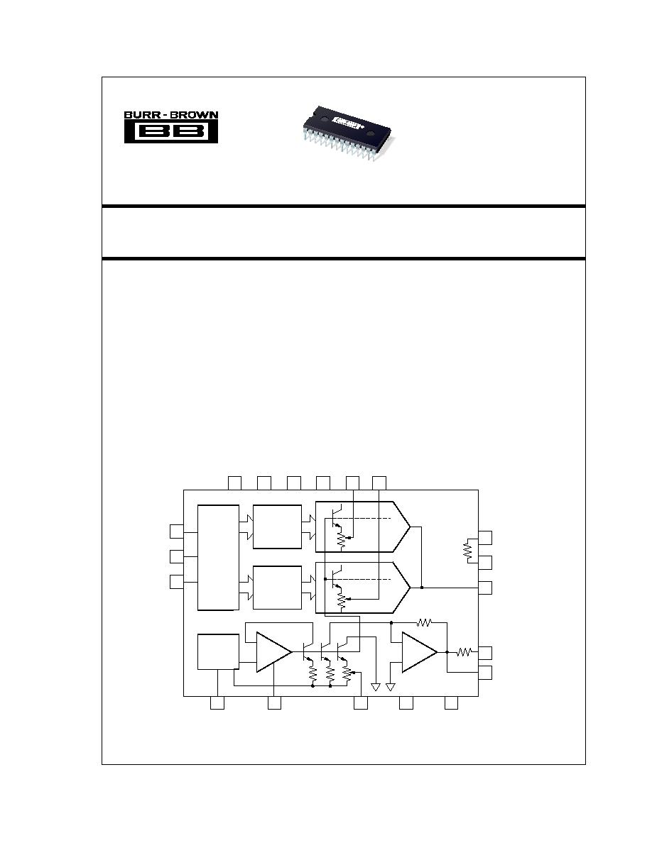
DESCRIPTION
The PCM63P is a precision 20-bit digital-to-analog
converter with ultra-low distortion (≠96dB max with a
full scale output; PCM63P-K). Incorporated into the
PCM63P is a unique
Colinear
dual-DAC per channel
architecture that eliminates unwanted glitches and
other nonlinearities around bipolar zero. The PCM63P
also features a very low noise (116dB max SNR;
A-weighted method) and fast settling current output
(200ns typ, 2mA step) which is capable of 16-times
oversampling rates.
Applications include very low distortion frequency
synthesis and high-end consumer and professional
digital audio applications.
Colinear
TM, Burr-Brown Corp.
Colinear
TM
20-Bit Monolithic Audio
DIGITAL-TO-ANALOG CONVERTER
Æ
19-Bit
Upper
DAC
19-Bit
Lower
DAC
Upper DAC
Positive
Data Latches
Lower DAC
Negative
Data Latches
Input Shift
Register
and
Control
Logic
Buried
Zener
Reference
Servo
Amp
Ref
Amp
PCM63P
20-Bit DAC
9
10
6
R
R
I
FEEDBACK
FEEDBACK
OUT
5
4
Bipolar Offset Current
Offset Decouple
25
7
12
Analog
Common
Digital
Common
3
1
Reference
Decouple
Servo
Decouple
18
20
21
Clock
Latch Enable
Data
23
24
Upper
B2 Adj
28
11
≠5V
Analog
2
13
+5V
Analog
Lower
B2 Adj
≠5V
Digital
+5V
Digital
Colinear
Potentiometer
Voltage
DEMO BOARD
AVAILABLE
See Appendix A
International Airport Industrial Park ∑ Mailing Address: PO Box 11400, Tucson, AZ 85734 ∑ Street Address: 6730 S. Tucson Blvd., Tucson, AZ 85706 ∑ Tel: (520) 746-1111 ∑ Twx: 910-952-1111
Internet: http://www.burr-brown.com/ ∑ FAXLine: (800) 548-6133 (US/Canada Only) ∑ Cable: BBRCORP ∑ Telex: 066-6491 ∑ FAX: (520) 889-1510 ∑ Immediate Product Info: (800) 548-6132
PCM63P
© 1990 Burr-Brown Corporation
PDS-1083F
Printed in U.S.A. January, 1998
2
Æ
PCM63P
The information provided herein is believed to be reliable; however, BURR-BROWN assumes no responsibility for inaccuracies or omissions. BURR-BROWN assumes
no responsibility for the use of this information, and all use of such information shall be entirely at the user's own risk. Prices and specifications are subject to change
without notice. No patent rights or licenses to any of the circuits described herein are implied or granted to any third party. BURR-BROWN does not authorize or warrant
any BURR-BROWN product for use in life support devices and/or systems.
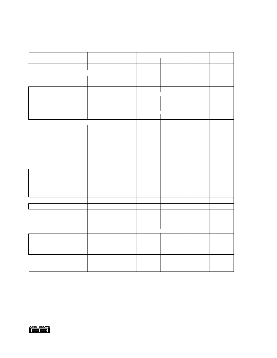
SPECIFICATIONS
ELECTRICAL
All specifications at 25
∞
C and
±
V
A
and
±
V
D
=
±
5V, unless otherwise noted.
PCM63P, PCM63P-J, PCM63P-K
PARAMETER
CONDITIONS
MIN
TYP
MAX
UNITS
RESOLUTION
20
Bits
DYNAMIC RANGE,
D
+
at ≠60dB Referred to Full Scale
PCM63P
96
100
dB
PCM63P-J
100
104
dB
PCM63P-K
104
108
dB
DIGITAL INPUT
Logic Family
TTL/CMOS Compatible
Logic Level: V
IH
+2.4
+V
D
V
V
IL
0
0.8
V
I
IH
V
IH
= +2.7V
+1
µ
A
I
IL
V
IL
= +0.4V
≠50
µ
A
Data Format
Serial, MSB First, BTC
(1)
Input Clock Frequency
12.5
25
MHz
TOTAL HARMONIC DISTORTION + N
(2)
, Without Adjustments
PCM63P
f = 991Hz (0dB)
(3)
f
S
= 352.8kHz
(4)
≠92
≠88
dB
f = 991Hz (≠20dB)
f
S
= 352.8kHz
≠80
≠74
dB
f = 991Hz (≠60dB)
f
S
= 352.8kHz
≠40
≠36
dB
PCM63P-J
f = 991Hz (0dB)
f
S
= 352.8kHz
≠96
≠92
dB
f = 991Hz (≠20dB)
f
S
= 352.8kHz
≠82
≠76
dB
f = 991Hz (≠60dB)
f
S
= 352.8kHz
≠44
≠40
dB
PCM63P-K
f = 991Hz (0dB)
f
S
= 352.8kHz
≠100
≠96
dB
f = 991Hz (≠20dB)
f
S
= 352.8kHz
≠88
≠82
dB
f = 991Hz (≠60dB)
f
S
= 352.8kHz
≠48
≠44
dB
ACCURACY
Level Linearity
at ≠90dB Signal Level
±
0.3
±
1
dB
Gain Error
±
1
±
2
%
Bipolar Zero Error
(5)
±
12
µ
A
Gain Drift
0
∞
C to 70
∞
C
25
ppm/
∞
C
Bipolar Zero Drift
0
∞
C to 70
∞
C
4
ppm of FSR/
∞
C
Warm-up Time
1
Minute
IDLE CHANNEL SNR
(6)
20Hz to 20kHz at BPZ
(7)
+116
+120
dB
POWER SUPPLY REJECTION
+86
dB
ANALOG OUTPUT
Output Range
±
2.00
mA
Output Impedance
670
Internal R
FEEDBACK
1.5
k
Settling Time
2mA Step
200
ns
Glitch Energy
No Glitch Around Zero
POWER SUPPLY REQUIREMENTS
±
V
A
,
±
V
D
Supply Voltage Range
±
4.50
±
5
±
5.50
V
+I
A
, +I
D
Combined Supply Current
+V
A
, +V
D
= +5V
10
15
mA
≠I
A
, ≠I
D
Combined Supply Current
≠V
A
, ≠V
D
= ≠5V
≠35
≠45
mA
Power Dissipation
±
V
A
,
±
V
D
=
±
5V
225
300
mW
TEMPERATURE RANGE
Specification
0
+70
∞
C
Operating
≠40
+85
∞
C
Storage
≠60
+100
∞
C
NOTES: (1) Binary Two's Complement coding. (2) Ratio of (Distortion
RMS
+ Noise
RMS
) / Signal
RMS
. (3) D/A converter output frequency (signal level). (4) D/A
converter sample frequency (8 x 44.1kHz; 8x oversampling). (5) Offset error at bipolar zero. (6) Measured using an OPA27 and 1.5k
feedback and an A-weighted
filter. (7) Bipolar Zero.
3
Æ
PCM63P
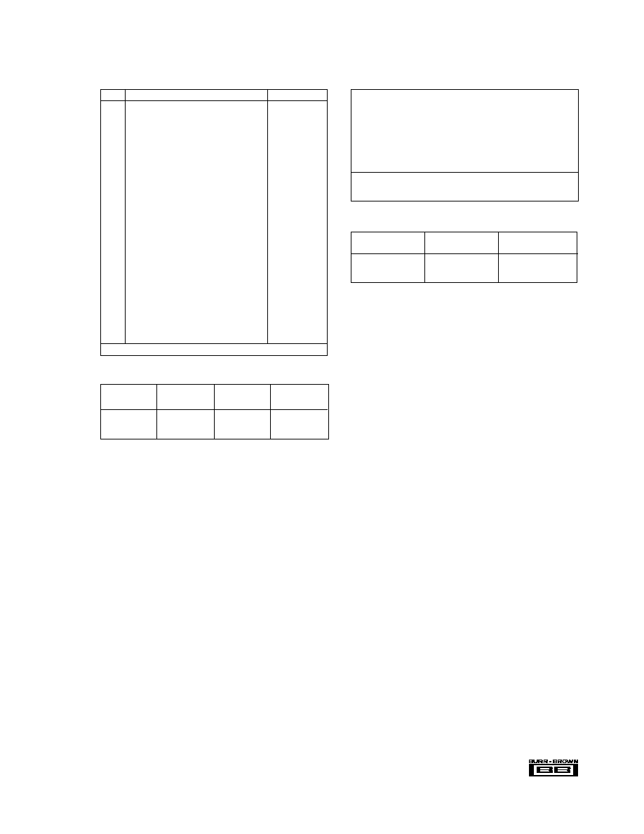
ORDERING INFORMATION
TEMPERATURE
MAX THD+N,
PRODUCT
PACKAGE
RANGE
AT 0dB
PCM63P
28-Pin Plastic DIP
0
∞
C to +70
∞
C
≠88dB
PCM63P-J
28-Pin Plastic DIP
0
∞
C to +70
∞
C
≠92dB
PCM63P-K
28-Pin Plastic DIP
0
∞
C to +70
∞
C
≠96dB
PIN ASSIGNMENTS
PIN
DESCRIPTION
MNEMONIC
P1
Servo Amp Decoupling Capacitor
CAP
P2
+5V Analog Supply Voltage
+V
A
P3
Reference Decoupling Capacitor
CAP
P4
Offset Decoupling Capacitor
CAP
P5
Bipolar Offset Current Output (+2mA)
BPO
P6
DAC Current Output (0 to ≠4mA)
I
OUT
P7
Analog Common Connection
ACOM
P8
No Connection
NC
P9
Feedback Resistor Connection (1.5k
)
RF
1
P10
Feedback Resistor Connection (1.5k
)
RF
2
P11
≠5V Digital Supply Voltage
≠V
D
P12
Digital Common Connection
DCOM
P13
+5V Digital Voltage Supply
+V
D
P14
No Connection
NC
P15
No Connection
NC
P16
No Connection
NC
P17
No Connection
NC
P18
DAC Data Clock Input
CLK
P19
No Connection
NC
P20
DAC Data Latch Enable
LE
P21
DAC Data Input
DATA
P22
No Connection
NC
P23
Optional Upper DAC Bit-2 Adjust (≠4.29V)*
UB2 Adj
P24
Optional Lower DAC Bit-2 Adjust (≠4.29V)*
LB2 Adj
P25
Bit Adjust Reference Voltage Tap (≠3.52V)*
V
POT
P26
No Connection
NC
P27
No Connection
NC
P28
≠5V Analog Supply Voltage
≠V
A
*Nominal voltages at these nodes assuming
±
V
A
;
±
V
D
=
±
5V.
ABSOLUTE MAXIMUM RATINGS
+V
A
, +V
D
to ACOM/DCOM ........................................................ 0V to +8V
≠V
A
, ≠V
D
to ACOM/DCOM ........................................................ 0V to ≠8V
≠V
A
, ≠V
D
to +V
A
, +V
D
............................................................. 0V to +16V
ACOM to DCOM ...............................................................................
±
0.5V
Digital Inputs (pins 18, 20, 21) to DCOM ............................... ≠1V to +V
D
Power Dissipation .......................................................................... 500mW
Lead Temperature, (soldering, 10s) .............................................. +300
∞
C
Max Junction Temperature .............................................................. 165
∞
C
Thermal Resistance,
JA
............................................................... 70
∞
C/W
NOTE: Stresses above those listed under "Absolute Maximum Ratings"
may cause permanent damage to the device. Exposure to absolute
maximum conditions for extended periods may affect device reliability.
PACKAGE INFORMATION
PACKAGE DRAWING
PRODUCT
PACKAGE
NUMBER
(1)
PCM63P
28-Pin Plastic DIP
215
PCM63P-J
28-Pin Plastic DIP
215
PCM63P-K
28-Pin Plastic DIP
215
NOTE: (1) For detailed drawing and dimension table, please see end of data
sheet, or Appendix C of Burr-Brown IC Data Book.
4
Æ
PCM63P
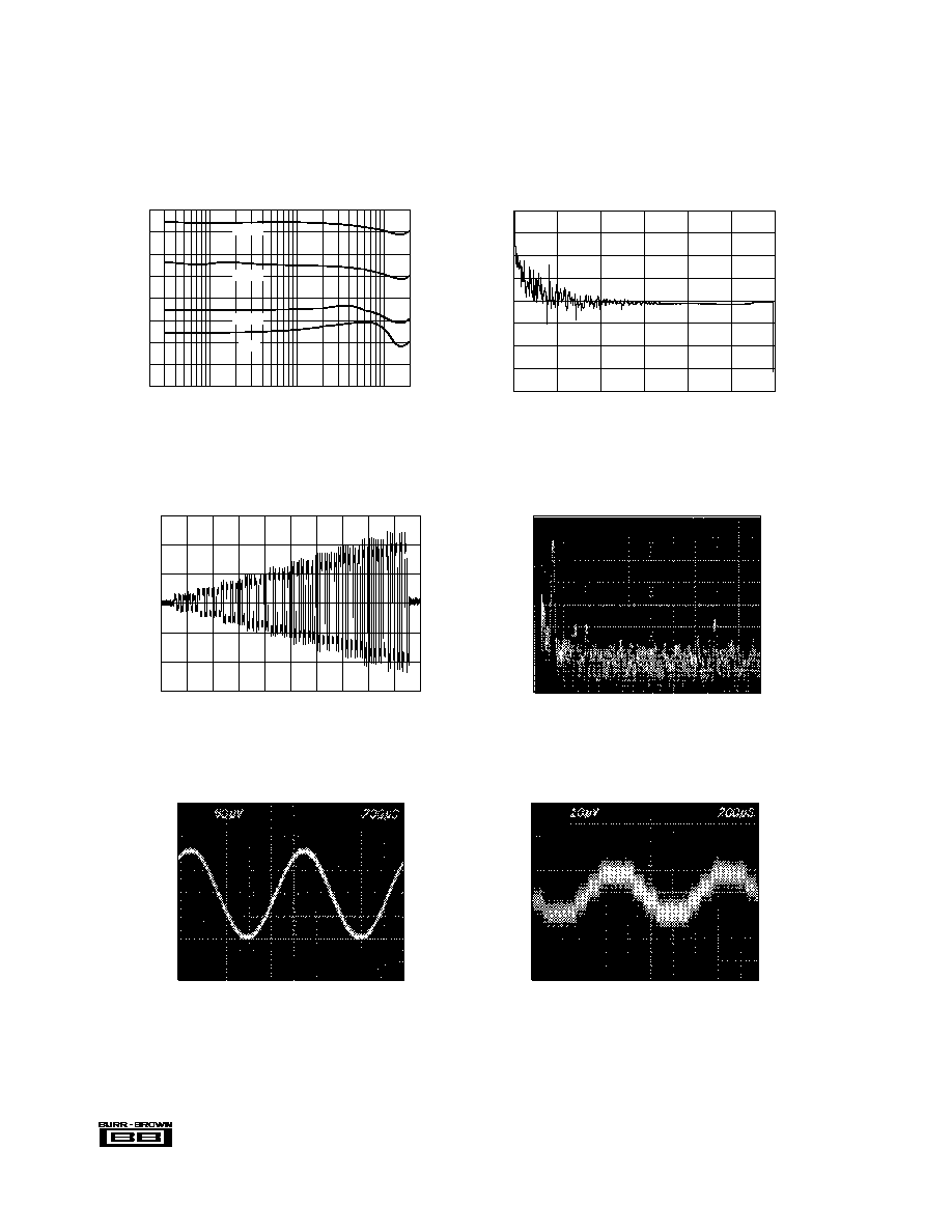
≠90dB SIGNAL
(10Hz to 20kHz Bandwidth)
200
100
0
≠100
≠200
Output Level (µV)
0
400
800
1200
1600
2000
Time (µs)
≠110dB SIGNAL
(10Hz to 20kHz Bandwidth)
40
20
0
≠20
≠40
Output Level (µV)
0
400
800
1200
1600
2000
Time (µs)
≠90dB SIGNAL SPECTRUM
(100Hz Bandwidth)
≠80
≠100
≠120
≠140
≠160
Power Spectrum (dB)
0
4k
8k
12k
16k
20k
Frequency (Hz)
TYPICAL PERFORMANCE CURVES
All specifications at 25
∞
C and
±
V
A
and
±
V
D
=
±
5.0V, unless otherwise noted.
FPO
FPO
FPO
16-BIT LEVEL LINEARITY
(Dithered Fade to Noise)
8
6
4
2
0
≠2
≠4
≠6
≠8
Deviation from Ideal Level (dB)
≠120
Output Signal Level (dB)
≠110
≠100
≠90
≠80
≠70
≠60
16-BIT MONOTONICITY
8.83ms/div
1.5
1
0.5
0
≠0.5
≠1
≠1.5
Output Voltage (mV)
THD+N vs FREQUENCY
≠40
≠60
≠100
≠120
≠80
20
100
1k
10k
Output Frequency (Hz)
THD+N (dB)
≠60dB
≠40dB
≠20dB
0dB
5
Æ
PCM63P
THEORY OF OPERATION
DUAL-DAC
COLINEAR ARCHITECTURE
Digital audio systems have traditionally used laser-trimmed,
current-source DACs in order to achieve sufficient accuracy.
However even the best of these suffer from potential low-
level nonlinearity due to errors at the major carry bipolar
zero transition. More recently, DACs employing a different
architecture which utilizes noise shaping techniques and
very high oversampling frequencies, have been introduced
("Bitstream", "MASH", or 1-bit DACs). These DACs over-
come the low level linearity problem, but only at the expense
of signal-to-noise performance, and often to the detriment of
channel separation and intermodulation distortion if the
succeeding circuitry is not carefully designed.
The PCM63 is a new solution to the problem. It combines all
the advantages of a conventional DAC (excellent full scale
performance, high signal-to-noise ratio and ease of use) with
superior low-level performance. Two DACs are combined
in a complementary arrangement to produce an extremely
linear output. The two DACs share a common reference and
a common R-2R ladder to ensure perfect tracking under all
conditions. By interleaving the individual bits of each DAC
and employing precise laser trimming of resistors, the highly
accurate match required between DACs is achieved.
This new, complementary linear or dual-DAC
Colinear
approach, which steps away from zero with small steps in
both directions, avoids any glitching or "large" linearity
errors and provides an absolute current output. The low level
performance of the PCM63P is such that real 20-bit resolu-
tion can be realized, especially around the critical bipolar
zero point.
Table I shows the conversion made by the internal logic of
the PCM63P from binary two's complement (BTC). Also,
the resulting internal codes to the upper and lower DACs
(see front page block diagram) are listed. Notice that only
the LSB portions of either internal DAC are changing
around bipolar zero. This accounts for the superlative per-
formance of the PCM63P in this area of operation.
DISCUSSION OF SPECIFICATIONS
DYNAMIC SPECIFICATIONS
Total Harmonic Distortion + Noise
The key specification for the PCM63P is total harmonic
distortion plus noise (THD+N). Digital data words are read
into the PCM63P at eight times the standard compact disk
audio sampling frequency of 44.1kHz (352.8kHz) so that a
sine wave output of 991Hz is realized. For production
testing, the output of the DAC goes to an I to V converter,
then to a programmable gain amplifier to provide gain at
lower signal output test levels, and then through a 40kHz
low pass filter before being fed into an analog type distortion
analyzer. Figure 1 shows a block diagram of the production
THD+N test setup.
For the audio bandwidth, THD+N of the PCM63P is essen-
tially flat for all frequencies. The typical performance curve,
"THD+N vs Frequency," shows four different output signal
levels: 0dB, ≠20dB, ≠40dB, and ≠60dB. The test signals are
derived from a special compact test disk (the CBS CD-1). It
is interesting to note that the ≠20dB signal falls only about
10dB below the full scale signal instead of the expected
20dB. This is primarily due to the superior low-level signal
performance of the dual-DAC
Colinear
architecture of the
PCM63P.
In terms of signal measurement, THD+N is the ratio of
Distortion
RMS
+ Noise
RMS
/ Signal
RMS
expressed in dB. For
the PCM63P, THD+N is 100% tested at all three specified
output levels using the test setup shown in Figure 1. It is
significant to note that this test setup does not include any
output deglitching circuitry. All specifications are achieved
without the use of external deglitchers.
Dynamic Range
Dynamic range in audio converters is specified as the measure
of THD+N at an effective output signal level of ≠60dB
referred to 0dB. Resolution is commonly used as a theoretical
measure of dynamic range, but it does not take into account
the effects of distortion and noise at low signal levels. The
INPUT CODE
LOWER DAC CODE
UPPER DAC CODE
ANALOG OUTPUT
(20-bit Binary Two's Complement)
(19-bit Straight Binary)
(19-bit Straight Binary)
+Full Scale
011...111
111...111 + 1LSB*
111...111
+Full Scale ≠ 1LSB
011...110
111...111 + 1LSB*
111...110
Bipolar Zero + 2LSB
000...010
111...111 + 1LSB*
000...010
Bipolar Zero + 1LSB
000...001
111...111 + 1LSB*
000...001
Bipolar Zero
000...000
111...111 + 1LSB*
000...000
Bipolar Zero ≠ 1LSB
111...111
111...111
000...000
Bipolar Zero ≠ 2LSB
111...110
111...110
000...000
≠Full Scale + 1LSB
100...001
000...001
000...000
≠Full Scale
100...000
000...000
000...000
*The extra weight of 1LSB is added at this point to make the transfer function symmetrical around bipolar zero.
TABLE I. Binary Two's Complement to
Colinear
Conversion Chart.
6
Æ
PCM63P
FIGURE 1. Production THD+N Test Setup.
Colinear
architecture of the PCM63P, with its ideal
performance around bipolar zero, provides a more usable
dynamic range, even using the strict audio definition, than
any previously available D/A converter.
Level Linearity
Deviation from ideal versus actual signal level is sometimes
called "level linearity" in digital audio converter testing. See
the "≠90dB Signal Spectrum" plot in the Typical Perfor-
mance Curves section for the power spectrum of a PCM63P
at a ≠90dB output level. (The "≠90dB Signal" plot shows the
actual ≠90dB output of the DAC). The deviation from ideal
for PCM63P at this signal level is typically less than
±
0.3dB.
For the "≠110dB Signal" plot in the Typical Performance
Curves section, true 20-bit digital code is used to generate a
≠110dB output signal. This type of performance is possible
only with the low-noise, near-theoretical performance around
bipolar zero of the PCM63P's
Colinear
DAC circuitry.
A commonly tested digital audio parameter is the amount of
deviation from ideal of a 1kHz signal when its amplitude is
decreased from ≠60dB to ≠120dB. A digitally dithered input
signal is applied to reach effective output levels of ≠120dB
using only the available 16-bit code from a special compact
disk test input. See the "16-Bit Level Linearity" plot in the
Typical Performance Curves section for the results of a
PCM63P tested using this 16-bit dithered fade-to-noise
signal. Note the very small deviation from ideal as the signal
goes from ≠60dB to ≠100dB.
DC SPECIFICATIONS
Idle Channel SNR
Another appropriate specification for a digital audio con-
verter is idle channel signal-to-noise ratio (idle channel
SNR). This is the ratio of the noise on the DAC output at
bipolar zero in relation to the full scale range of the DAC. To
make this measurement, the digital input is continuously fed
the code for bipolar zero while the output of the DAC is
band-limited from 20Hz to 20kHz and an A-weighted filter
is applied. The idle channel SNR for the PCM63P is typi-
cally greater than 120dB, making it ideal for low-noise
applications.
Monotonicity
Because of the unique dual-DAC
Colinear
architecture of
the PCM63P, increasing values of digital input will always
result in increasing values of DAC output as the signal
moves away from bipolar zero in one-LSB steps (in either
direction). The "16-Bit Monotonicity" plot in the Typical
Performance Curves section was generated using 16-bit
digital code from a test compact disk. The test starts with 10
periods of bipolar zero. Next are 10 periods of alternating
1LSBs above and below zero, and then 10 periods of
alternating 2LSBs above and below zero, and so on until
10LSBs above and below zero are reached. The signal
pattern then begins again at bipolar zero.
With PCM63P, the low-noise steps are clearly defined and
increase in near-perfect proportion. This performance is
achieved without any external adjustments. By contrast,
sigma-delta ("Bitstream", "MASH", or 1-bit DAC) architec-
tures are too noisy to even see the first 3 or 4 bits change (at
16 bits), other than by a change in the noise level.
Absolute Linearity
Even though absolute integral and differential linearity specs
are not given for the PCM63P, the extremely low THD+N
performance is typically indicative of 16-bit to 17-bit inte-
gral linearity in the DAC, depending on the grade specified.
The relationship between THD+N and linearity, however, is
not such that an absolute linearity specification for every
individual output code can be guaranteed.
Distortion
Analyzer
Use 400Hz High-Pass
Filter and 30kHz
Low-Pass Filter
Meter Settings
Programmable
Gain Amp
0dB to 60dB
Low-Pass
Filter
40kHz 3rd Order
GIC Type
DUT
(PCM63P)
Parallel-to-Serial
Conversion
Digital Code
(EPROM)
Binary
Counter
Timing
Logic
Clock
Latch Enable
Sampling Rate = 44.1kHz x 8 (352.8kHz)
Output Frequency = 991Hz
(Shiba Soku Model
725 or Equivalent)
I to V
Converter
OPA627
7
Æ
PCM63P
Offset, Gain, And Temperature Drift
Although the PCM63P is primarily meant for use in dy-
namic applications, specifications are also given for more
traditional DC parameters such as gain error, bipolar zero
offset error, and temperature gain and offset drift.
DIGITAL INPUT
Timing Considerations
The PCM63P accepts TTL compatible logic input levels.
Noise immunity is enhanced by the use of differential
current mode logic input architectures on all input signal
lines. The data format of the PCM63P is binary two's
complement (BTC) with the most significant bit (MSB)
being first in the serial input bit stream. Table II describes
the exact relationship of input data to voltage output coding.
Any number of bits can precede the 20 bits to be loaded,
since only the last 20 will be transferred to the parallel DAC
register after LE (P20, Latch Enable) has gone low.
All DAC serial input data (P21, DATA) bit transfers are
triggered on positive clock (P18, CLK) edges. The serial-to-
parallel data transfer to the DAC occurs on the falling edge
of Latch Enable (P20, LE). The change in the output of the
DAC coincides with the falling edge of Latch Enable (P20,
LE). Refer to Figure 2 for graphical relationships of these
signals.
Maximum Clock Rate
A typical clock rate of 16.9MHz for the PCM63P is derived
by multiplying the standard audio sample rate of 44.1kHz by
sixteen times (16
x
oversampling) the standard audio word
bit length of 24 bits (44.1kHz
x
16
x
24 = 16.9MHz). Note
that this clock rate accommodates a 24-bit word length, even
though only 20 bits are actually being used. The maximum
clock rate of 25MHz is guaranteed, but is not 100% final
tested. The setup and hold timing relationships are shown in
Figure 3.
"Stopped Clock" Operation
The PCM63P is normally operated with a continuous clock
input signal. If the clock is to be stopped between input data
words, the last 20 bits shifted in are not actually shifted from
the serial register to the latched parallel DAC register until
Latch Enable (LE, P20) goes low. Latch Enable must remain
low until after the first clock cycle of the next data word
to insure proper DAC operation. In any case, the setup and
hold times for Data and LE must be observed as shown in
Figure 3.
FIGURE 2. Timing Diagram.
NOTES: (1) If clock is stopped between input of 20-bit data words, Latch Enable (LE) must remain low until after the first clock cycle of the next 20-bit data
word stream. (2) Data format is binary two's complement (BTC). Individual data bits are clocked in on the corresponding positive clock edge. (3) Latch Enable
(LE) must remain low at least one clock cycle after going negative. (4) Latch Enable (LE) must be high for at least one clock cycle before going negative.
(5) I
OUT
changes on negative going edge of Latch Enable (LE).
P18 (Clock)
P21 (Data)
P20 (Latch Enable)
P6 (I )
1
2
3
12
13
14
15
16
17
18
19
20
4
1
MSB
LSB
OUT
VOLTAGE OUTPUT
DIGITAL INPUT
ANALOG OUTPUT
CURRENT OUTPUT
(With External Op Amp)
1,048,576LSBs
Full Scale Range
4.00000000mA
6.00000000V
1LSB
NA
3.81469727nA
5.72204590
µ
V
7FFFF
HEX
+Full Scale
≠1.99999619mA
+2.99999428V
00000
HEX
Bipolar Zero
0.00000000mA
0.00000000V
FFFFF
HEX
Bipolar Zero ≠ 1LSB
+0.00000381mA
≠0.00000572V
80000
HEX
≠Full Scale
+2.00000000mA
≠3.00000000V
TABLE II. Digital Input/Output Relationships.
FIGURE 3. Setup and Hold Timing Diagram.
Data
Input
Clock
Input
Latch
Enable
LSB
MSB
>One Clock Cycle
>20ns
>10ns
>15ns
>15ns
>1ns
>33ns
>10ns
>One Clock Cycle
>10ns
8
Æ
PCM63P
INSTALLATION
POWER SUPPLIES
Refer to Figure 4 for proper connection of the PCM63P in
the voltage-out mode using the internal feedback resistor.
The feedback resistor connections (P9 and P10) should be
left open if not used. The PCM63P only requires a
±
5V
supply. Both positive supplies should be tied together at a
single point. Similarly, both negative supplies should be
connected together. No real advantage is gained by using
separate analog and digital supplies. It is more important that
both these supplies be as "clean" as possible to reduce
coupling of supply noise to the output. Power supply decou-
pling capacitors should be used at each supply pin to
maximize power supply rejection, as shown in Figure 4,
regardless of how good the supplies are. Both commons
should be connected to an analog ground plane as close to
the PCM63P as possible.
FILTER CAPACITOR REQUIREMENTS
As shown in Figure 4, various size decoupling capacitors
can be used, with no special tolerances being required. The
size of the offset decoupling capacitor is not critical either,
with larger values (up to 100
µ
F) giving slightly better SNR
readings. All capacitors should be as close to the appropriate
pins of the PCM63P as possible to reduce noise pickup from
surrounding circuitry.
MSB ADJUSTMENT CIRCUITRY
Near optimum performance can be maintained at all signal
levels without using the optional MSB adjust circuitry of the
PCM63P shown in Figure 5. Adjustability is provided for
those cases where slightly better full-scale THD+N is
desired. Use of the MSB adjustments will only affect larger
dynamic signals (between 0dB and ≠6dB). This improve-
ment comes from bettering the gain match between the
upper and lower DACs at these signal levels. The change is
realized by small adjustments in the bit-2 weights of each
DAC. Great care should be taken, however, as improper
adjustment will easily result in degraded performance.
In theory, the adjustments would seem very simple to
perform, but in practice they are actually quite complex. The
first step in the theoretical procedure would involve making
each bit-2 weight ideal in relation to its code minus one
value (adjusting each potentiometer for zero differential
nonlinearity error at the bit-2 major carries). This would be
the starting point of each 100k
potentiometer for the next
adjustment. Then, each potentiometer would be adjusted
equally, in opposite directions, to achieve the lowest full-
scale THD+N possible (reversing the direction of rotation
FIGURE 5. Optional Bit-2 Adjustment Circuitry.
0.1µF
330k
330k
0.1µF
100k
100k
28
25
24
23
≠V
V
LB2 Adj
UB2 Adj
A
POT
FIGURE 4. Connection Diagram.
1
2
3
4
5
6
7
8
9
10
11
12
13
14
28
27
26
25
24
23
22
21
20
19
18
17
16
15
CAP
+V
CAP
CAP
BPO
I
ACOM
NC
RF
RF
≠V
DCOM
+V
NC
≠V
NC
NC
V
LB2 Adj
UB2 Adj
NC
DATA
LE
NC
CLK
NC
NC
NC
PCM63P
A
1µF
0.1µF
4.7µF
+
1µF
1µF
1/2
OPA2604
OUT
1
2
D
D
A
POT
1µF
0.1µF
0.1µF
≠5V
+5V
0.1µF
±3V

9
Æ
PCM63P
for both if no immediate improvement were noted). This
procedure would require the generation of the digital bit-2
major carry code to the input of the PCM63P and a DVM or
oscilloscope capable of reading the output voltage for a one
LSB step (5.72
µ
V) in addition to a distortion analyzer.
A more practical approach would be to forego the minor
correction for the bit-2 major carry adjustment and only
adjust for upper and lower DAC gain matching. The prob-
lem is that just by connecting the MSB circuitry to the
PCM63P, the odds are that the upper and lower bit-2 weights
would be greatly changed from their unadjusted states and
thereby adversely affect the desired gain adjustment. Just
centering the 100k
potentiometers would not necessarily
provide the correct starting point. To guarantee that each
100k
potentiometer would be set to the correct starting or
null point (no current into or out of the MSB adjust pins), the
voltage drop across each corresponding 330k
resistor would
have to measure 0V. A voltage drop of
±
1.25mV across
either 330k
resistor would correspond to a
±
1LSB change
in the null point from its unadjusted state (1LSB in current
or 3.81nA
x
330k
= 1.26mV). Once these starting points
for each potentiometer had been set, each potentiometer
would then be adjusted equally, in opposite directions, to
achieve the lowest full-scale THD+N possible. If no imme-
diate improvement were noted, the direction of rotation for
both potentiometers would be reversed. One direction of
potentiometer counter-rotations would only make the gain
mismatch and resulting THD+N worse, while the opposite
would gradually improve and then worsen the THD+N after
passing through a no mismatch point. The determination of
the correct starting direction would be arbitrary. This proce-
dure still requires a good DVM in addition to a distortion
analyzer.
Each user will have to determine if a small improvement in
full-scale THD+N for their application is worth the expense
of performing a proper MSB adjustment.
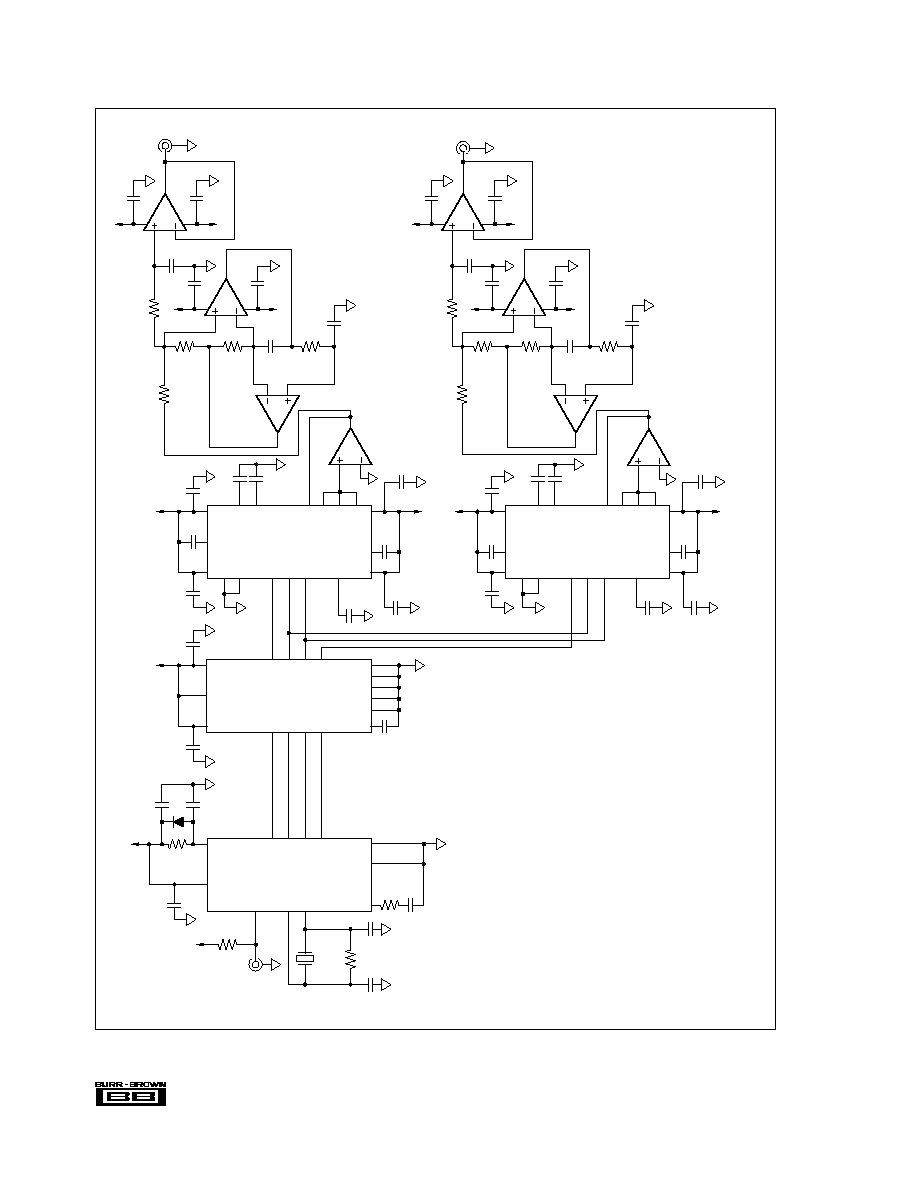
APPLICATIONS
The most common application for the PCM63P is in high-
performance and professional digital audio playback, such
as in CD and DAT players. The circuit in Figure 6 shows the
PCM63P in a typical combination with a digital interface
format receiver chip (Yamaha YM3623), an 8
x
interpolating
digital filter (Burr-Brown DF1700P), and two third-order
low-pass anti-imaging filters (implemented using Burr-Brown
OPA2604APs).
Using an 8
x
digital filter increases the number of samples to
the DAC by a factor of 8, thereby reducing the need for a
higher order reconstruction or anti-imaging analog filter on
the DAC output. An analog filter can now be constructed
using a simple phase-linear GIC (generalized immittance
converter) architecture. Excellent sonic performance is
achieved using a digital filter in the design, while reducing
overall circuit complexity at the same time.
Because of its superior low-level performance, the PCM63P
is also ideally suited for other high-performance applications
such as direct digital synthesis (DDS).
10
Æ
PCM63P
1M
16.9344MHz
20-Bit D/A
Converter
0.1µF
31
3
2
1µF
1µF
+5V
24
0.1µF
23
0.1µF
12
7
0.1µF
12
8
11
1µF
≠5V
4.7µF
+
4
1µF
10
5
6
9
20
18
21
20-Bit D/A
Converter
0.1µF
31
3
2
1µF
1µF
+5V
24
0.1µF
23
0.1µF
12
7
0.1µF
12
8
11
1µF
≠5V
4.7µF
+
4
10
5
6
9
20
18
21
8X Interpolation
Digital Filter
17
22
3
+5V
23
100pF
14
21
16
4.7µF
1
28
2
26
25
24
4.7µF
6
10
4
Digital Interface
Format Receiver
17
+5V
8
4700pF
31
4
5
6
12
15
17
0.1µF
28
4
4.7µF
17.1k
+5V
(192F )
S
10pF
10pF
Interleaved
Digital
Input
150
A
BCO
L/R
DA
Yamaha
YM3623
Burr-Brown
PCM63P
Burr-Brown
PCM63P
Burr-Brown
DF1700P
8
4.7µF
+
+
4.7µF
+5V
≠5V
1
8
3
2
4.7µF
+
+
4.7µF
+5V
≠5V
1
8
3
2
1000pF
1.33k
7.23k
7.23k
1000pF
3.47k
6
5
1000pF
1µF
4.7µF
+
+
4.7µF
+5V
≠5V
1
8
3
2
4.7µF
+
+
4.7µF
+5V
≠5V
1
8
3
2
1000pF
1.33k
7.23k
1000pF
3.47k
6
5
1000pF
7
7
3.92k
3.92k
7.23k
4
4
4
4
DOR
BCO
WCK
DOL
4.7µF
DATA
CLK
LE
DATA
CLK
LE
±3V
V
Right
OUT
A
1
A
2
A
2
A
1
7
5
6
A
3
A
4
7
5
6
A
4
A
3
±3V
V
Left
OUT
+
+
A , A , A , A = Burr-Brown OPA2604AP,
or equivalent.
12
3
4
+
FIGURE 6. Stereo Audio Application.