 | –≠–ª–µ–∫—Ç—Ä–æ–Ω–Ω—ã–π –∫–æ–º–ø–æ–Ω–µ–Ω—Ç: SHC804 | –°–∫–∞—á–∞—Ç—å:  PDF PDF  ZIP ZIP |
1
Æ
SHC804
SHC804
Æ
©
1983 Burr-Brown Corporation
PDS-512E
Printed in U.S.A. March, 1998
Switch
Drive
Sample/Hold
Analog Input
Sample/
Hold
Output
Hold
Analog
Common
1000
1000
C
H
International Airport Industrial Park ∑ Mailing Address: PO Box 11400, Tucson, AZ 85734 ∑ Street Address: 6730 S. Tucson Blvd., Tucson, AZ 85706 ∑ Tel: (520) 746-1111 ∑ Twx: 910-952-1111
Internet: http://www.burr-brown.com/ ∑ FAXLine: (800) 548-6133 (US/Canada Only) ∑ Cable: BBRCORP ∑ Telex: 066-6491 ∑ FAX: (520) 889-1510 ∑ Immediate Product Info: (800) 548-6132
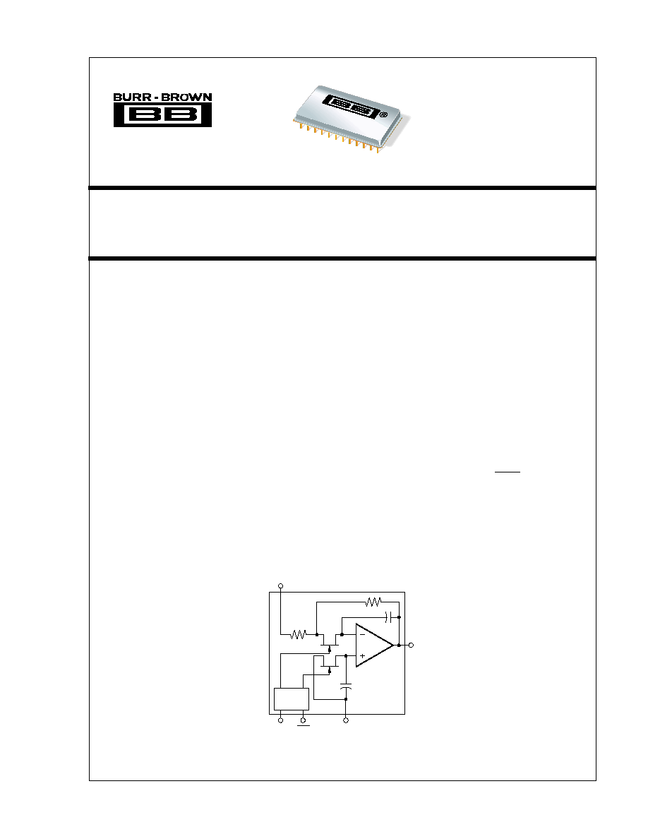
High Speed
SAMPLE/HOLD AMPLIFIER
FEATURES
q
350ns max ACQUISITION TIME
q
±
0.01% THROUGHPUT NONLINEARITY
q
150ns max SAMPLE-TO-HOLD SETTLING
TIME
q
24-PIN HERMETICALLY-SEALED METAL
PACKAGE
The
±
25ps maximum aperture uncertainty of the
SHC804 permits sampling (to
±
0.01% of Full Scale
Range) of signals with rates of change of up to 100V/
µ
s.
This component is capable of accurately digitizing fast
changing signals at sample rates as high as 500k
samples per second.
The digital inputs (HOLD and HOLD) are TTL-
compatible. Power supply requirements are
±
15V and
+5V and the specification temperature range is ≠25
∞
C
to +85
∞
C. The SHC804 is packaged in a 24-pin dual-
in-line hermetic metal package. SHC804 is pin-com-
patible with other sample/holds on the market with
similar performance characteristics.
DESCRIPTION
The SHC804 is a high speed sample/hold amplifier
designed for use in fast 12-bit data acquisition systems
and signal processing systems.
The SHC804 acquires a 10V signal change in less than
350ns to
±
1/2LSB at 12 bits. Throughput nonlinearity
error is guaranteed to be within
±
1/2LSB for 12-bit
systems. Stability over temperature is excellent, with
only
±
5ppm/
∞
C of gain drift and
±
4ppm of FSR/
∞
C of
charge offset drift over the ≠25 to +85
∞
C temperature
range.
SHC804
2
Æ
SHC804
SPECIFICATIONS
At +25
∞
C, rated power supplies and a 1k
output load, unless otherwise specified.
SHC804BM
SHC804CM
PARAMETER
MIN
TYP
MAX
MIN
TYP
MAX
UNITS
SAMPLE/HOLD INPUTS (without Input Buffer)
ANALOG
Voltage Range
±
10.25
±
11
T
T
V
R
IN
1.00
T
k
DIGITAL (HOLD, HOLD)
V
IH
+2.0
T
V
V
IL
+0.8
T
V
I
IH
, V
IN
= +2.7V
+60
T
µ
A
I
IL
, V
IN
= +0.4V
≠1.2
T
mA
SAMPLE/HOLD TRANSFER CHARACTERISTICS (without Input Buffer)
ACCURACY
Sample Mode
Gain
≠1
T
V/V
Gain Error
±
0.1
T
%
Temperature Coefficient
±
3
±
10
±
1
±
5
ppm/
∞
C
Linearity Error
±
0.001
±
0.005
T
T
% of FSR
(1)
Zero Offset
±
1
±
5
±
0.5
±
3
mV
Temperature Coefficient
±
1
±
2.5
±
0.5
±
1.5
ppm of FSR/
∞
C
Hold Mode
Charge Offset
±
2
±
10
±
1
±
5
mV
Temperature Coefficient
±
3
±
10
±
2
±
4
ppm of FSR/
∞
C
Droop Rate: at +25
∞
C
±
0.5
±
5
T
T
µ
V/
µ
s
+85
∞
C
±
0.5
±
0.1
mV/
µ
s
Throughput Nonlinearity
±
0.01
T
% of FSR
Power Supply Sensitivity
(2)
:
±
V
CC
±
0.002
T
% of FSR/%V
CC
V
DD
±
0.003
T
% of FSR/%V
DD
DYNAMIC CHARACTERISTICS
Acquisition Time (with 10V Step)
to within:
±
0.1% (
±
10mV)
220
T
ns
±
0.01% (
±
1mV)
250
350
T
T
ns
Sample-to-Hold Settling Time
to within
±
0.01% (
±
1mV)
100
150
T
T
ns
Sample-to-Hold Transient Amplitude
60
150
T
T
mV
PEAK
Aperture Delay TIme
(3)
15
25
T
T
ns
Aperture Uncertainty
±
10
±
25
T
T
ps
Sample Mode: Output Slew Rate
160
T
V/
µ
s
Full Power Bandwidth
1
T
MHz
Small Signal Bandwidth
16
T
MHz
Hold Mode Feedthrough Rejection
(10V Square Wave Input)
±
0.03
±
0.005
T
%
SAMPLE/HOLD OUTPUT
Voltage Range
±
10.25
±
11
T
T
V
Output Current
±
50
T
mA
Short Circuit Protection
Indefinite to Common
T
Output Impedance (at DC)
0.01
0.1
T
T
POWER SUPPLY REQUIREMENTS
Rated Voltage:
±
V
CC
±
13.5
±
15
±
16.5
T
T
T
V
V
DD
+4.75
+5.00
+5.25
T
T
T
V
Quiescent Current (No Load)
SHC804: +V
CC
30
35
T
T
mA
≠V
CC
15
20
T
T
mA
V
DD
5
10
T
T
mA
SHC803: +V
CC
33
40
T
T
mA
≠V
CC
18
25
T
T
mA
V
DD
5
10
T
T
mA
Power Dissipation: SHC804
700
875
T
T
mW
TEMPERATURE RANGE
Specification
≠25
+85
T
T
∞
C
Storage
≠55
+125
T
T
∞
C
T
Specification same as SHC804BM.
NOTES: (1) FSR means Full Scale Range and is 20V for SHC804. (2) Sensitivity of offset plus charge offset. (3) With respect to HOLD. For HOLD add 5ns typical.
(4) With buffer connected to the sample/hold amplifier.
3
Æ
SHC804
Input Overvoltage ..............................................................................
±
15V
+V
CC
to V
CC
COMMON .............................................................. 0 to +18V
≠V
CC
to V
CC
COMMON .............................................................. 0 to ≠18V
Voltage on Digital Inputs (pins 11 and 12) ........................... ≠0.5V to +7V
Power Dissipation ....................................................................... 1500mW
V
DD
to DCOM ................................................................................... ≠0.5V
Analog Output ............................................... Indefinite Short to V
CC
COM
ABSOLUTE MAXIMUM RATINGS
(1)
PACKAGE INFORMATION
PACKAGE DRAWING
PRODUCT
PACKAGE
NUMBER
(1)
SHC804BM
24-Pin
037
SHC804CM
24-Pin
037
NOTE: (1) For detailed drawing and dimension table, please see end of data
sheet, or Appendix C of Burr-Brown IC Data Book.
NOTE: Stresses above those listed under "Absolute Maximum Ratings" may
cause permanent damage to the device. Exposure to absolute maximum
conditions for extended periods may affect device reliability.
CONNECTION DIAGRAMS
Analog
Output
1
2
3
4
5
6
7
8
9
10
11
12
24
23
22
21
20
19
18
17
16
15
14
13
NC
NC
NC
NC
NC
NC
NC
V
DD
DCOM
Hold
Hold
+V
CC
V
CC
COM
≠V
CC
COM
NC
NC
NC
NC
NC
COM
S/H In
Digital
Power
Supply
COM
Analog
Power
Supply
+15V
COM
≠15V
1µF
1µF
Signal
Source
V
OUT
SHC804CM, BM
+5V
NC
The information provided herein is believed to be reliable; however, BURR-BROWN assumes no responsibility for inaccuracies or omissions. BURR-BROWN assumes
no responsibility for the use of this information, and all use of such information shall be entirely at the user's own risk. Prices and specifications are subject to change
without notice. No patent rights or licenses to any of the circuits described herein are implied or granted to any third party. BURR-BROWN does not authorize or warrant
any BURR-BROWN product for use in life support devices and/or systems.
PIN
NAME
DESCRIPTION
1
Sample/Hold Output
Analog voltage output
2
NC
Not connected
3
NC
Not connected
4
NC
Not connected
5
NC
Not connected
6
NC
Not connected
7
NC
Not connected
8
NC
Not connected
9
V
DD
Logic supply
10
DCOM
Logic supply common
11
HOLD
Logic "1" = HOLD
12
HOLD
Logic "0" = HOLD
13
S/H In
SHC804 input
14
NC
Not connected
15
COM
Signal common
16
NC
Not connected
17
NC
Not connected
18
NC
Not connected
19
NC
Not connected
20
NC
Not connected
21
COM
Signal common
22
≠V
CC
≠15V supply
23
V
CC
COM
Analog to power common, connected
to case
24
+V
CC
+15V supply
PIN ASSIGNMENTS
ELECTROSTATIC
DISCHARGE SENSITIVITY
This integrated circuit can be damaged by ESD. Burr-Brown
recommends that all integrated circuits be handled with
appropriate precautions. Failure to observe proper handling
and installation procedures can cause damage.
ESD damage can range from subtle performance degradation
to complete device failure. Precision integrated circuits may
be more susceptible to damage because very small parametric
changes could cause the device not to meet its published
specifications.
4
Æ
SHC804
INSTALLATION
GROUNDING AND BYPASSING
SHC804 has four COMMON pins (pins 10, 15, 21 and 23)
and all must be tied together and connected to the system
analog common (V
CC
COM) as close to the package as
possible. It is preferable to have a large ground plane
surrounding the sample/hold and have all four common pins
soldered directly to it. Note that the metal case is internally
connected to pin 23; therefore, care must be taken to avoid
a ground loop if the case is allowed to contact the ground
plane.
Most digital return currents pass through pin 10. Noise from
the switch-drive circuit may couple directly into the main op
amp summing junction, a very noise-sensitive node. Care
must be taken to insure that no voltage differences occur
between pin 10 and the other common pins. This is the
reason pin 10 must be connected directly to the ground
plane.
For the same reason, the logic supply should be kept as free
of noise as possible.
±
V
CC
supply lines (pins 24 and 22) are
internally bypassed to common with 0.01
µ
F capacitors. It is
recommended that the user install additional external 0.1
µ
F
to 1
µ
F tantalum bypass capacitors at each supply pin.
SAMPLE/HOLD CONTROL
A TTL logic "0" at pin 11 (or a logic "1" at pin 12) switches
the SHC804 into the Sample (track) mode. In this mode, the
device acts as a unity-gain inverting amplifier, the output
following the inverse of the input. A logic "1" at pin 11 (or
a logic "0" at pin 12) will switch the SHC804 into the Hold
mode. The output voltages will be held constant at the value
present when the Hold command is given.
If pin 11 is used, pin 12 must be connected to the DCOM
(pin 10). If pin 12 is used, pin 11 must be tied to V
DD
. Using
the HOLD and HOLD inputs as logic function may ad-
versely affect the charge offset (pedestal). A clean digital
signal (no overshoot) at the HOLD of HOLD inputs will
also reduce charge offset errors. Pins 11 and 12 present less
than one standard TTL load (two LSTTL loads) to the digital
drive circuit.
DISCUSSION OF
SPECIFICATIONS
Throughput Nonlinearity is defined as total Hold mode,
nonadjustable, input to output error caused by charge offset,
gain nonlinearity, droop, feedthrough, and thermal tran-
sients. It is the inaccuracy due to these errors which cannot
be corrected by Offset and Gain adjustments.
Gain Error is the difference between the input and output
voltage magnitude (in the Sample mode) due to the amplifier
gain errors.
Droop Rate is the voltage decay at the output when in the
Hold mode due to storage capacitor and FET switch leakage
current and the input bias current of the output amplifier.
Feedthrough is the amount of output voltage change caused
by an input voltage change when the sample/hold is in the
Hold mode.
Aperture Delay Time is the time required to switch from
Sample to Hold. The time is measured from the 50% point
of the Hold mode control transition to the time at which the
output stops tracking the input.
Aperture Uncertainty Time is the nonrepeatability of aper-
ture delay time.
Acquisition Time is the time required for the sample/hold
output to settle to within a given error band of its final value
when the sample/hold is switched from Hold to Sample.
Charge Offset (Pedestal) is the output voltage change that
results from charge coupled into the Hold capacitor through
the gate capacitance of the switching field effect transistor.
This charge appears as an offset at the output.
Sample-to-Hold Switching Transient is the switching tran-
sient which appears on the output when the sample/hold is
switched from Sample to Hold. Both the magnitude and the
settling time of the transient are specified.
OPERATION
In the Sample (track) mode the circuit acts as a unity-gain
inverting amplifier. In the Hold mode, the capacitor, C
H
,
holds the value of the output at the time the unit was
switched to the Hold mode. Additional circuits compensate
for switching transients and provide switch leakage current
cancellation. The amplifier provides high current drive and
low output impedance to external loads.
GAIN, OFFSET, CHARGE OFFSET
SHC804 has been internally-trimmed to eliminate the need
for external trim potentiometers for Gain, Offset (in Sample
mode) and Charge Offset (Pedestal). System Gain and Off-
set errors can be adjusted elsewhere in the system, at an
input amplifier preceding the sample/hold, or at an analog-
to-digital converter following the sample/hold.
Droop
V
OUT
Acquisition
Time
Sample
Hold
V
IN
Sample-to-Hold
Transient
V
t
FIGURE 1. Definition of Acquisition Time, Droop and
Sample-to-Hold Transient.

5
Æ
SHC804
OUTPUT LOADING
Care must be taken when loading the output of the SHC804
to avoid possible oscillations, current limiting and perfor-
mance variations over temperature.
The maximum capacitive load to avoid oscillations is about
300pF. Recommended resistive load is 500
or more, al-
though values as low as 250
may be used. Acquisition and
sample-to-hold settling times are relatively unaffected by
resistive loads down to 250
in parallel with capacitive
loads up to 100pF. Higher capacitances will affect acquisi-
tion and settling times.
ANALOG SIGNAL SOURCE CONSIDERATIONS
The output impedance of the signal source driving the
SHC804 will affect the accuracy of the sample and hold
operation both statically (at DC) and dynamically. The
output impedance of the signal source should be low and
remain low over a wide bandwidth. A small capacitor at the
driving source may help to improve the charge offset errors
that are affected by dynamic source impedance.