
A
3 Watt LCS Single Series DC/DC Converters
2401 Stanwell Drive ∑ Concord, California 94520 ∑ Ph: 925/687-4411 or 800/542-3355 ∑ Fax: 925/687-3333 ∑ www.calex.com ∑ Email: sales@calex.com
1
1/29/04, eco#041007-1, eco# 050628-1, 060403-7
3 Watt LCS Single Series Block Diagram
Features
Up to 3 Watts in a 0.80" x 1.25" x 0.28" case
Low Cost
Standard Pinout
Wide Input Range
High Efficiency
Fully Isolated, 1544 VDC
Fully Self contained,
No External Parts Required for Operation
5 Year Warranty
Description
These 3 Watt DC/DC converters were designed for fast
integration with your system's power needs. With no external
components or filtering necessary for all but the most critical
applications, these converters can provide power instantly.
This saves you costly engineering time required to design
your system around the power converter.
t
r
a
h
C
n
o
i
t
c
e
l
e
S
l
e
d
o
M
e
g
n
a
R
t
u
p
n
I
C
D
V
t
u
o
V
C
D
V
t
u
o
I
A
m
n
i
M
m
o
N
x
a
M
S
C
L
0
0
6
.
3
R
3
S
2
1
9
2
1
8
1
3
.
3
0
0
6
S
C
L
0
0
6
.
5
S
2
1
9
2
1
8
1
5
0
0
6
S
C
L
0
5
2
.
2
1
S
2
1
9
2
1
8
1
2
1
0
5
2
S
C
L
0
0
2
.
5
1
S
2
1
9
2
1
8
1
5
1
0
0
2
S
C
L
0
0
6
.
3
R
3
S
4
2
8
1
4
2
6
3
3
.
3
0
0
6
S
C
L
0
0
6
.
5
S
4
2
8
1
4
2
6
3
5
0
0
6
S
C
L
0
5
2
.
2
1
S
4
2
8
1
4
2
6
3
2
1
0
5
2
S
C
L
0
0
2
.
5
1
S
4
2
8
1
4
2
6
3
5
1
0
0
2
S
C
L
0
0
6
.
3
R
3
S
8
4
6
3
8
4
2
7
3
.
3
0
0
6
S
C
L
0
0
6
.
5
S
8
4
6
3
8
4
2
7
5
0
0
6
S
C
L
0
5
2
.
2
1
S
8
4
6
3
8
4
2
7
2
1
0
5
2
S
C
L
0
0
2
.
5
1
S
8
4
6
3
8
4
2
7
5
1
0
0
2

A
3 Watt LCS Single Series DC/DC Converters
2401 Stanwell Drive ∑ Concord, California 94520 ∑ Ph: 925/687-4411 or 800/542-3355 ∑ Fax: 925/687-3333 ∑ www.calex.com ∑ Email: sales@calex.com
2
1/29/04, eco#041007-1, eco# 050628-1, 060403-7
NOTES
*
All parameters measured at T
AMB
= 25∞C, nominal input
voltage and full rated load unless otherwise noted. Refer
to the CALEX Application Notes for the definition of
terms, measurement circuits and other information.
(2)
Noise is measured per CALEX Application Notes. Measurement
bandwidth is 0-20 MHz for peak-peak measurements, 10 kHz to
1 MHz for RMS measurements. Output noise is measured with
a 0.01µF / 100V ceramic capacitor in parallel with a 1µf / 35V
Tantalum capacitor, 1 inch from the output pins to simulate
standard PCB decoupling capacitance.
(3)
External fusing should be used for system protection due to a
catastrophic failure. See CALEX Application Note 9 in the Calex
DC/DC Catalog to determine correct fuse.
)
1
(
*
s
r
e
t
e
m
a
r
a
P
t
u
p
n
I
l
e
d
o
M
S
C
L
0
0
6
.
3
R
3
S
2
1
S
C
L
0
0
6
.
5
S
2
1
S
C
L
0
5
2
.
2
1
S
2
1
S
C
L
0
0
2
.
5
1
S
2
1
s
t
i
n
U
e
g
n
a
R
e
g
a
t
l
o
V
N
I
M
P
Y
T
X
A
M
9
2
1
8
1
C
D
V
d
a
o
L
o
N
t
n
e
r
r
u
C
t
u
p
n
I
d
a
o
L
n
i
M
d
a
o
L
ll
u
F
P
Y
T
P
Y
T
P
Y
T
0
1
3
3
1
3
2
0
1
0
5
8
3
3
0
1
0
5
1
2
3
4
1
0
5
0
1
3
A
m
y
c
n
e
i
c
i
f
f
E
P
Y
T
0
7
4
7
8
7
0
8
%
y
c
n
e
u
q
e
r
F
g
n
i
h
c
t
i
w
S
P
Y
T
0
0
3
z
H
k
,
e
g
a
t
l
o
v
r
e
v
O
t
u
p
n
I
m
u
m
i
x
a
M
m
u
m
i
x
a
M
s
m
0
0
1
4
2
C
D
V
,
e
m
i
T
n
o
-
n
r
u
T
r
o
r
r
E
t
u
p
t
u
O
%
1
1
s
m
e
s
u
F
d
e
d
n
e
m
m
o
c
e
R
)
3
(
l
e
d
o
M
S
C
L
0
0
6
.
3
R
3
S
4
2
S
C
L
0
0
6
.
5
S
4
2
S
C
L
0
5
2
.
2
1
S
4
2
S
C
L
0
0
2
.
5
1
S
4
2
s
t
i
n
U
e
g
n
a
R
e
g
a
t
l
o
V
N
I
M
P
Y
T
X
A
M
8
1
4
2
6
3
C
D
V
d
a
o
L
o
N
t
n
e
r
r
u
C
t
u
p
n
I
d
a
o
L
n
i
M
d
a
o
L
ll
u
F
P
Y
T
P
Y
T
P
Y
T
2
7
1
1
1
1
2
5
2
1
6
1
2
5
2
5
5
1
2
5
2
5
5
1
A
m
y
c
n
e
i
c
i
f
f
E
P
Y
T
3
7
8
7
0
8
0
8
%
y
c
n
e
u
q
e
r
F
g
n
i
h
c
t
i
w
S
P
Y
T
0
0
3
z
H
k
,
e
g
a
t
l
o
v
r
e
v
O
t
u
p
n
I
m
u
m
i
x
a
M
m
u
m
i
x
a
M
s
m
0
0
1
5
4
C
D
V
,
e
m
i
T
n
o
-
n
r
u
T
r
o
r
r
E
t
u
p
t
u
O
%
1
1
s
m
e
s
u
F
d
e
d
n
e
m
m
o
c
e
R
)
3
(
l
e
d
o
M
S
C
L
0
0
6
.
3
R
3
S
8
4
S
C
L
0
0
6
.
5
S
8
4
S
C
L
0
5
2
.
2
1
S
8
4
S
C
L
0
0
2
.
5
1
S
8
4
s
t
i
n
U
e
g
n
a
R
e
g
a
t
l
o
V
N
I
M
P
Y
T
X
A
M
6
3
8
4
2
7
C
D
V
d
a
o
L
o
N
t
n
e
r
r
u
C
t
u
p
n
I
d
a
o
L
n
i
M
d
a
o
L
ll
u
F
P
Y
T
P
Y
T
P
Y
T
2
7
7
5
2
3
1
1
8
2
3
1
7
7
2
3
1
7
7
A
m
y
c
n
e
i
c
i
f
f
E
P
Y
T
3
7
8
7
0
8
0
8
%
y
c
n
e
u
q
e
r
F
g
n
i
h
c
t
i
w
S
P
Y
T
0
0
3
z
H
k
,
e
g
a
t
l
o
v
r
e
v
O
t
u
p
n
I
m
u
m
i
x
a
M
m
u
m
i
x
a
M
s
m
0
0
1
5
8
C
D
V
,
e
m
i
T
n
o
-
n
r
u
T
r
o
r
r
E
t
u
p
t
u
O
%
1
1
s
m
e
s
u
F
d
e
d
n
e
m
m
o
c
e
R
)
3
(
(4)
The case thermal impedance is specified as the case temperature
rise over ambient per package watt dissipated.
(5)
Specifications subject to change without notice.
(6)
Requires minimum load to regulate. No harm to the unit when
operated at less than minimum load.
(7)
Water Washability - Calex DC/DC converters are designed to
withstand most solder/wash processes. Careful attention should
be used when assessing the applicability in your specific
manufacturing process. Converters are not hermetically sealed.
A
3 Watt LCS Single Series DC/DC Converters
2401 Stanwell Drive ∑ Concord, California 94520 ∑ Ph: 925/687-4411 or 800/542-3355 ∑ Fax: 925/687-3333 ∑ www.calex.com ∑ Email: sales@calex.com
3
1/29/04, eco#041007-1, eco# 050628-1, 060403-7
n
i
P
n
o
i
t
c
n
u
F
2
T
U
P
N
I
-
3
T
U
P
N
I
-
9
N
M
C
T
U
P
T
U
O
1
1
T
U
P
T
U
O
+
4
1
T
U
P
T
U
O
+
6
1
N
M
C
T
U
P
T
U
O
2
2
T
U
P
N
I
+
3
2
T
U
P
N
I
+
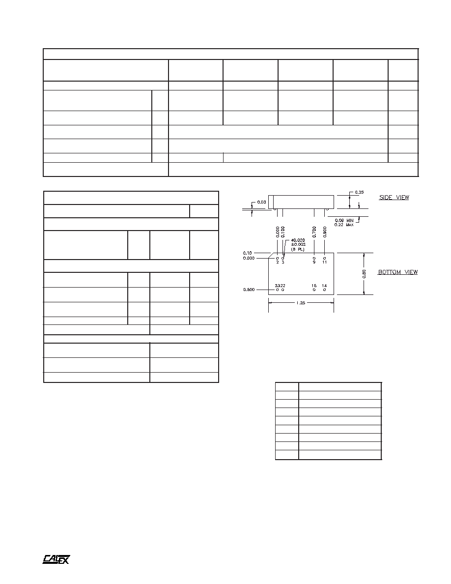
Mechanical tolerances unless otherwise noted:
X.XX dimensions: ±0.020 inches
X.XXX dimensions: ±0.005 inches
Pin location shown is for mating PCB.
The case is plastic with a non-conductive header.
)
1
(
*
s
r
e
t
e
m
a
r
a
P
t
u
p
t
u
O
l
e
d
o
M
S
C
L
0
0
6
.
3
R
3
S
2
1
S
C
L
0
0
6
.
3
R
3
S
4
2
S
C
L
0
0
6
.
3
R
3
S
8
4
S
C
L
0
0
6
.
5
S
2
1
S
C
L
0
0
6
.
5
S
4
2
S
C
L
0
0
6
.
5
S
8
4
S
C
L
0
5
2
.
2
1
S
2
1
S
C
L
0
5
2
.
2
1
S
4
2
S
C
L
0
5
2
.
2
1
S
8
4
S
C
L
0
0
2
.
5
1
S
2
1
S
C
L
0
0
2
.
5
1
S
4
2
S
C
L
0
0
2
.
5
1
S
8
4
s
t
i
n
U
e
g
a
t
l
o
V
t
u
p
t
u
O
3
.
3
5
2
1
5
1
C
D
V
y
c
a
r
u
c
c
A
e
g
a
t
l
o
V
t
u
p
t
u
O
N
I
M
P
Y
T
X
A
M
4
2
.
3
3
3
.
3
2
4
.
3
0
9
.
4
0
0
.
5
0
1
.
5
0
7
.
1
1
0
0
.
2
1
0
3
.
2
1
0
6
.
4
1
0
0
.
5
1
0
4
.
5
1
C
D
V
)
6
(
e
g
n
a
R
d
a
o
L
d
e
t
a
R
N
I
M
X
A
M
0
6
0
0
6
0
6
0
0
6
5
2
0
5
2
0
2
0
0
2
A
m
n
o
i
t
a
l
u
g
e
R
d
a
o
L
d
a
o
L
%
0
0
1
-
%
0
1
P
Y
T
2
.
0
%
n
o
i
t
a
l
u
g
e
R
e
n
i
L
C
D
V
x
a
M
-
n
i
M
=
n
i
V
P
Y
T
1
.
0
%
)
2
(
e
s
i
o
N
P
Y
T
0
5
5
7
P
-
P
V
m
n
o
i
t
c
e
t
o
r
P
t
i
u
c
r
i
C
t
r
o
h
S
t
r
a
t
s
e
R
o
t
u
A
,
s
u
o
u
n
i
t
n
o
C
APPLICATION NOTE
Start-up: A minimum load is required for the LCS to have a
nominal output. The specification indicates a minimum load of
10% of the maximum load, but will usually start with less. The
type of load will also vary the start-up characteristics. Such as
an electronic load or some types of active circuitry (vs. a pure
resisitive load) will require more load for start-up.
Each application should be verified and an additional resistive
load added if needed.
The output may be in a burp mode (output pulsing) with less
than a minimum load, causing the output voltage to vary.
s
n
o
i
t
a
c
i
f
i
c
e
p
S
l
a
r
e
n
e
G
s
l
e
d
o
M
l
l
A
s
t
i
n
U
n
o
i
t
a
l
o
s
I
,
n
o
i
t
a
l
o
s
I
t
u
p
t
u
O
o
t
t
u
p
n
I
e
g
a
k
a
e
L
µ
0
1
V
4
2
,
V
2
1
=
m
o
n
V
V
8
4
=
m
o
n
V
N
I
M
N
I
M
0
0
7
4
4
5
1
C
D
V
C
D
V
l
a
t
n
e
m
n
o
r
i
v
n
E
g
n
i
t
a
r
e
p
O
t
n
e
i
b
m
A
e
r
u
t
a
r
e
p
m
e
T
N
I
M
X
A
M
0
4
-
5
8
+
C
∞
e
r
u
t
a
r
e
p
m
e
T
g
n
i
t
a
r
e
p
O
e
s
a
C
N
I
M
X
A
M
0
4
-
5
0
1
+
C
∞
e
r
u
t
a
r
e
p
m
e
T
e
g
a
r
o
t
S
N
I
M
X
A
M
0
4
-
5
2
1
+
C
∞
)
4
(
e
c
n
a
d
e
p
m
I
l
a
m
r
e
h
T
P
Y
T
0
3
t
t
a
w
/
C
∞
g
n
il
o
o
C
n
o
i
t
c
e
v
n
o
C
r
i
A
-
e
e
r
F
l
a
r
e
n
e
G
e
z
i
S
e
s
a
C
n
i
8
2
.
0
x
4
7
.
0
x
7
2
.
1
m
m
1
.
7
x
8
.
8
1
x
3
.
2
3
l
a
i
r
e
t
a
M
e
s
a
C
e
v
i
t
c
u
d
n
o
C
-
n
o
N
c
i
t
s
a
l
P
k
c
a
l
B
t
h
g
i
e
W
g
8