
A
10 Watt NT Single Series DC/DC Converters
2401 Stanwell Drive ∑ Concord, California 94520 ∑ Ph: 925/687-4411 or 800/542-3355 ∑ Fax: 925/687-3333 ∑ www.calex.com ∑ Email: sales@calex.com
1
eco# 041007-1, 060831-1
10 Watt NT Single Series Block Diagram
Features
Fully Self Contained, No External Parts Required
for Operation
Low and Specified Input/Output Capacitance
Efficiencies to 85%
Overcurrent Protected for Long, Reliable Operation
Five-sided, Shielded, Low Thermal Gradient
Copper Case
Water Washable Case Design
Five Year Warranty
Description
These 10 Watt DC/DC converters were designed for fast
integration with your system's power needs. With no external
components or filtering necessary for all but the most critical
applications, these converters can provide power instantly.
This saves you costly engineering time required to design
your system around the power converter.
t
r
a
h
C
n
o
i
t
c
e
l
e
S
l
e
d
o
M
e
g
n
a
R
t
u
p
n
I
C
D
V
t
u
p
t
u
O
C
D
V
t
u
p
t
u
O
A
m
n
i
M
x
a
M
T
N
0
0
0
2
.
3
S
2
1
9
8
1
3
3
.
3
0
0
0
2
T
N
0
0
0
2
.
5
S
2
1
9
8
1
5
0
0
0
2
T
N
0
0
9
.
2
1
S
2
1
9
8
1
2
1
0
0
9
T
N
0
0
7
.
5
1
S
2
1
9
8
1
5
1
0
0
7
T
N
0
0
0
2
.
3
S
4
2
8
1
6
3
3
3
.
3
0
0
0
2
T
N
0
0
0
2
.
5
S
4
2
*
8
1
6
3
5
0
0
0
2
T
N
0
0
9
.
2
1
S
4
2
8
1
6
3
2
1
0
0
9
T
N
0
0
7
.
5
1
S
4
2
8
1
6
3
5
1
0
0
7
T
N
0
0
0
2
.
3
S
8
4
*
6
3
2
7
3
3
.
3
0
0
0
2
T
N
0
0
0
2
.
5
S
8
4
*
6
3
2
7
5
0
0
0
2
T
N
0
0
9
.
2
1
S
8
4
*
6
3
2
7
2
1
0
0
9
T
N
0
0
7
.
5
1
S
8
4
*
6
3
2
7
5
1
0
0
7
T
N
0
0
5
1
.
5
S
8
4
0
2
0
6
5
0
0
5
1
0
5
9
0
6
L
U
/
A
S
C
:
s
l
a
v
o
r
p
p
A
y
c
n
e
g
A
*

A
10 Watt NT Single Series DC/DC Converters
2401 Stanwell Drive ∑ Concord, California 94520 ∑ Ph: 925/687-4411 or 800/542-3355 ∑ Fax: 925/687-3333 ∑ www.calex.com ∑ Email: sales@calex.com
2
eco# 041007-1, 060831-1
NOTES
*
All parameters measured at Tc = 25∞C, nominal input voltage
and full rated load unless otherwise noted. Refer to the
CALEX Application Notes for the definition of terms,
measurement circuits and other information.
(2)
Noise is measured per CALEX Application Notes. Measurement
bandwidth is 0-20 MHz for peak-peak measurements, 10 kHz to
1 MHz for RMS measurements. Output noise is measured with
a 0.01µF / 100V ceramic capacitor in parallel with a 1µf / 35V
Tantalum capacitor, 1 inch from the output pins to simulate
standard PCB decoupling capacitance.
(3)
To determine the correct fuse size, see CALEX Application
Notes.
(4)
The Case is tied to the -input pin.
(5)
Short term stability is specified after a 30 minute warmup at full
load, constant line and recording the drift over a 24 hour period.
(6)
The transient response is specified as the time required to settle
from a 50 to 75 % step load change (rise time of step = 2 µSec)
to a 1% error band.
*
s
r
e
t
e
m
a
r
a
P
t
u
p
n
I
l
e
d
o
M
T
N
0
0
0
2
.
3
S
2
1
T
N
0
0
0
2
.
5
S
2
1
T
N
0
0
9
.
2
1
S
2
1
T
N
0
0
7
.
5
1
S
2
1
T
N
0
0
0
2
.
3
S
4
2
T
N
0
0
0
2
.
5
S
4
2
s
t
i
n
U
e
g
n
a
R
e
g
a
t
l
o
V
N
I
M
X
A
M
9
8
1
8
1
6
3
C
D
V
)
2
(
e
l
p
p
i
R
d
e
t
c
e
l
f
e
R
P
Y
T
0
8
2
0
4
4
0
4
1
0
1
2
P
-
P
A
m
P
Y
T
0
9
5
4
1
5
4
0
7
S
M
R
A
m
d
a
o
L
ll
u
F
t
n
e
r
r
u
C
t
u
p
n
I
d
a
o
L
o
N
P
Y
T
P
Y
T
0
1
7
7
0
7
0
1
7
0
0
1
1
2
1
0
6
0
1
5
1
0
4
3
7
0
0
5
7
A
m
y
c
n
e
i
c
i
f
f
E
P
Y
T
8
7
8
7
2
8
3
8
2
8
3
8
%
y
c
n
e
u
q
e
r
F
g
n
i
h
c
t
i
w
S
P
Y
T
0
2
2
z
H
k
,
e
g
a
t
l
o
v
r
e
v
O
t
u
p
n
I
m
u
m
i
x
a
M
m
u
m
i
x
a
M
s
m
0
0
1
X
A
M
4
2
5
4
C
D
V
,
e
m
i
T
n
o
-
n
r
u
T
r
o
r
r
E
t
u
p
t
u
O
%
1
P
Y
T
6
s
m
e
s
u
F
d
e
d
n
e
m
m
o
c
e
R
)
3
(
S
P
M
A
l
e
d
o
M
T
N
0
0
9
.
2
1
S
4
2
T
N
0
0
7
.
5
1
S
4
2
T
N
0
0
0
2
.
3
S
8
4
T
N
0
0
0
2
.
5
S
8
4
T
N
0
0
9
.
2
1
S
8
4
T
N
0
0
7
.
5
1
S
8
4
s
t
i
n
U
e
g
n
a
R
e
g
a
t
l
o
V
N
I
M
X
A
M
8
1
6
3
6
3
2
7
C
D
V
)
2
(
e
l
p
p
i
R
d
e
t
c
e
l
f
e
R
P
Y
T
0
1
2
0
0
1
0
5
1
P
-
P
A
m
P
Y
T
0
7
5
3
0
5
S
M
R
A
m
d
a
o
L
ll
u
F
t
n
e
r
r
u
C
t
u
p
n
I
d
a
o
L
o
N
P
Y
T
P
Y
T
0
3
5
0
1
0
1
5
0
1
0
7
1
6
0
6
2
6
0
7
2
6
0
6
2
6
A
m
y
c
n
e
i
c
i
f
f
E
P
Y
T
5
8
6
8
0
8
1
8
3
8
4
8
%
y
c
n
e
u
q
e
r
F
g
n
i
h
c
t
i
w
S
P
Y
T
0
2
2
z
H
k
,
e
g
a
t
l
o
v
r
e
v
O
t
u
p
n
I
m
u
m
i
x
a
M
m
u
m
i
x
a
M
s
m
0
0
1
X
A
M
5
4
5
8
C
D
V
,
e
m
i
T
n
o
-
n
r
u
T
r
o
r
r
E
t
u
p
t
u
O
%
1
P
Y
T
6
s
m
e
s
u
F
d
e
d
n
e
m
m
o
c
e
R
)
3
(
S
P
M
A
l
e
d
o
M
T
N
0
0
5
1
.
5
S
8
4
s
t
i
n
U
e
g
n
a
R
e
g
a
t
l
o
V
N
I
M
X
A
M
0
2
0
6
C
D
V
)
2
(
e
l
p
p
i
R
d
e
t
c
e
l
f
e
R
P
Y
T
0
3
1
P
-
P
A
m
P
Y
T
0
4
S
M
R
A
m
d
a
o
L
ll
u
F
t
n
e
r
r
u
C
t
u
p
n
I
d
a
o
L
o
N
P
Y
T
P
Y
T
0
0
2
6
A
m
y
c
n
e
i
c
i
f
f
E
P
Y
T
8
7
%
y
c
n
e
u
q
e
r
F
g
n
i
h
c
t
i
w
S
P
Y
T
0
2
2
z
H
k
,
e
g
a
t
l
o
v
r
e
v
O
t
u
p
n
I
m
u
m
i
x
a
M
m
u
m
i
x
a
M
s
m
0
0
1
X
A
M
2
7
C
D
V
,
e
m
i
T
n
o
-
n
r
u
T
r
o
r
r
E
t
u
p
t
u
O
%
1
P
Y
T
6
s
m
e
s
u
F
d
e
d
n
e
m
m
o
c
e
R
)
3
(
S
P
M
A
(7)
Dynamic response is the peak overshoot during a transient
as defined in note 6 above.
(8)
The input ripple rejection is specified for DC to 120 Hz ripple with
a modulation amplitude of 1% of Vin.
(9)
The functional temperature range is intended to give an additional
data point for use in evaluating this power supply. At the
low functional temperature the power supply will function with
no side effects, however, sustained operation at the high
functional temperature will reduce expected operational life.
The data sheet specifications are not guaranteed over the
functional temperature range.
(10) The case thermal impedance is specified as the case temperature
rise over ambient per package watt dissipated.
(11) Specifications subject to change without notice.
(12) Water Washability - Calex DC/DC converters are designed to
withstand most solder/wash processes. Careful attention should
be used when assessing the applicability in your specific
manufacturing process. Converters are not hermetically sealed.
A
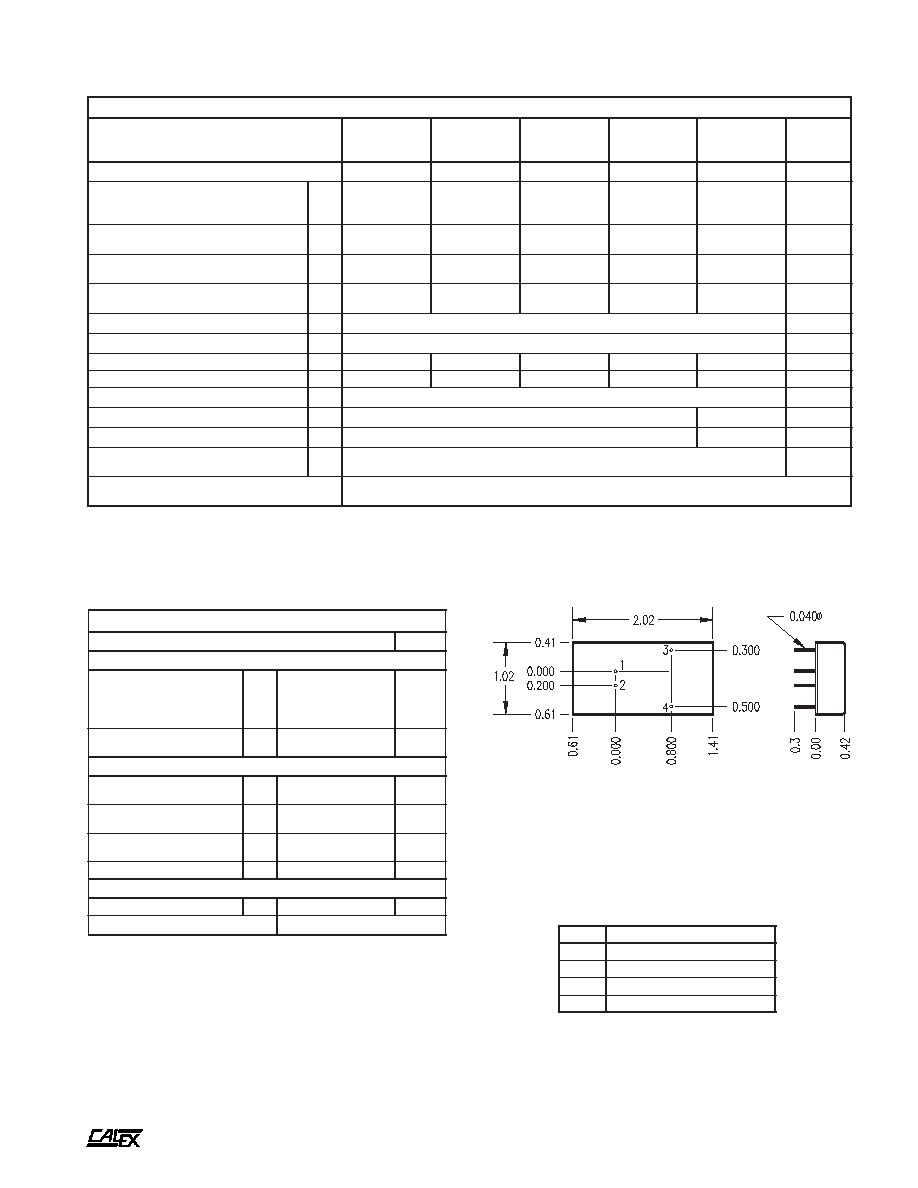
10 Watt NT Single Series DC/DC Converters
2401 Stanwell Drive ∑ Concord, California 94520 ∑ Ph: 925/687-4411 or 800/542-3355 ∑ Fax: 925/687-3333 ∑ www.calex.com ∑ Email: sales@calex.com
3
eco# 041007-1, 060831-1
±0.002
n
i
P
n
o
i
t
c
n
u
F
1
T
U
P
N
I
+
2
T
U
P
N
I
-
3
T
U
P
T
U
O
+
4
N
M
C
Mechanical tolerances unless otherwise noted:
X.XX dimensions: ±0.020 inches
X.XXX dimensions: ±0.005 inches
BOTTOM VIEW
SIDE VIEW
*
s
r
e
t
e
m
a
r
a
P
t
u
p
t
u
O
l
e
d
o
M
T
N
0
0
0
2
.
3
S
2
1
T
N
0
0
0
2
.
3
S
4
2
T
N
0
0
0
2
.
3
S
8
4
T
N
0
0
0
2
.
5
S
2
1
T
N
0
0
0
2
.
5
S
4
2
T
N
0
0
0
2
.
5
S
8
4
T
N
0
0
9
.
2
1
S
2
1
T
N
0
0
9
.
2
1
S
4
2
T
N
0
0
9
.
2
1
S
8
4
T
N
0
0
7
.
5
1
S
2
1
T
N
0
0
7
.
5
1
S
4
2
T
N
0
0
7
.
5
1
S
8
4
T
N
0
0
5
1
.
5
S
8
4
s
t
i
n
U
e
g
a
t
l
o
V
t
u
p
t
u
O
3
3
.
3
5
2
1
5
1
5
C
D
V
y
c
a
r
u
c
c
A
e
g
a
t
l
o
V
t
u
p
t
u
O
N
I
M
P
Y
T
X
A
M
0
3
.
3
3
3
.
3
6
3
.
3
5
9
.
4
0
0
.
5
5
0
.
5
0
9
.
1
1
0
0
.
2
1
0
1
.
2
1
0
9
.
4
1
0
0
.
5
1
0
1
.
5
1
5
9
.
4
0
0
.
5
5
0
.
5
C
D
V
e
g
n
a
R
d
a
o
L
d
e
t
a
R
N
I
M
X
A
M
2
.
0
0
.
2
0
.
0
0
.
2
0
.
0
9
.
0
0
.
0
7
.
0
0
.
0
5
.
1
A
n
o
i
t
a
l
u
g
e
R
d
a
o
L
d
a
o
L
x
a
M
-
d
a
o
L
x
a
M
%
5
2
P
Y
T
X
A
M
1
.
0
4
.
0
1
.
0
4
.
0
2
.
0
4
.
0
2
.
0
4
.
0
1
.
0
3
.
0
%
n
o
i
t
a
l
u
g
e
R
e
n
i
L
C
D
V
x
a
M
-
n
i
M
=
n
i
V
P
Y
T
X
A
M
5
.
0
0
.
1
1
0
.
0
2
.
0
2
.
0
8
.
0
2
.
0
8
.
0
1
0
.
0
2
.
0
%
)
5
(
y
t
il
i
b
a
t
S
m
r
e
T
t
r
o
h
S
P
Y
T
5
0
.
0
<
s
r
H
4
2
/
%
y
t
il
i
b
a
t
S
m
r
e
T
g
n
o
L
P
Y
T
1
.
0
<
s
r
H
k
/
%
)
6
(
e
s
n
o
p
s
e
R
t
n
e
i
s
n
a
r
T
P
Y
T
0
0
1
0
5
2
0
5
2
0
0
4
0
0
5
s
µ
)
7
(
e
s
n
o
p
s
e
R
c
i
m
a
n
y
D
P
Y
T
0
3
1
0
9
0
5
2
0
5
3
5
2
1
k
a
e
p
V
m
)
8
(
n
o
i
t
c
e
j
e
R
e
l
p
p
i
R
t
u
p
n
I
P
Y
T
0
4
>
B
d
)
2
(
k
a
e
P
-
k
a
e
P
,
e
s
i
o
N
P
Y
T
0
6
5
7
P
-
P
V
m
e
s
i
o
N
S
M
R
P
Y
T
6
5
S
M
R
V
m
t
n
e
i
c
i
f
f
e
o
C
e
r
u
t
a
r
e
p
m
e
T
P
Y
T
X
A
M
0
5
0
5
1
C
∞
/
m
p
p
o
t
n
o
i
t
c
e
t
o
r
P
t
i
u
c
r
i
C
t
r
o
h
S
s
t
u
p
t
u
O
ll
a
r
o
f
n
o
m
m
o
C
n
o
i
t
c
e
t
o
r
P
t
i
m
i
L
t
n
e
r
r
u
C
,
s
u
o
u
n
i
t
n
o
C
*
s
n
o
i
t
a
c
i
f
i
c
e
p
S
l
a
r
e
n
e
G
s
l
e
d
o
M
l
l
A
s
t
i
n
U
)
4
(
n
o
i
t
a
l
o
s
I
e
g
a
t
l
o
V
n
o
i
t
a
l
o
s
I
S
4
2
,
S
2
1
t
u
p
t
u
O
o
t
t
u
p
n
I
S
8
4
t
u
p
t
u
O
o
t
t
u
p
n
I
e
g
a
k
a
e
L
A
µ
0
1
N
I
M
N
I
M
0
0
7
4
4
5
1
C
D
V
t
u
p
t
u
O
o
t
t
u
p
n
I
e
c
n
a
t
i
c
a
p
a
C
P
Y
T
0
0
4
F
p
l
a
t
n
e
m
n
o
r
i
v
n
E
e
g
n
a
R
g
n
i
t
a
r
e
p
O
e
s
a
C
g
n
i
t
a
r
e
D
o
N
N
I
M
X
A
M
0
4
-
0
9
C
∞
)
9
(
e
g
n
a
R
l
a
n
o
i
t
c
n
u
F
e
s
a
C
N
I
M
X
A
M
0
5
-
0
0
1
C
∞
e
g
n
a
R
e
g
a
r
o
t
S
N
I
M
X
A
M
5
5
-
5
0
1
C
∞
)
0
1
(
e
c
n
a
d
e
p
m
I
l
a
m
r
e
h
T
P
Y
T
5
1
t
t
a
W
/
C
∞
l
a
r
e
n
e
G
t
h
g
i
e
W
t
i
n
U
P
Y
T
0
.
1
z
o
t
i
K
g
n
i
t
n
u
o
M
s
i
s
s
a
h
C
5
1
S
M
,
8
S
M
,
6
S
M

A
10 Watt NT Single Series DC/DC Converters
2401 Stanwell Drive ∑ Concord, California 94520 ∑ Ph: 925/687-4411 or 800/542-3355 ∑ Fax: 925/687-3333 ∑ www.calex.com ∑ Email: sales@calex.com
4
eco# 041007-1, 060831-1
3
4
1
2
Figure 1.
Standard connections for the 10 Watt NT Single. The input fuse
should not be omitted. The overvoltage diodes D1 and D2 may be
added to the circuit directly at the converter to provide transient
protection to your circuit.
No external capacitance on the output is required for
normal operation. In fact, it can degrade the converter's
performance. See our application note "Understanding DC/
DC Converters Output Impedance" and the low noise circuits
for more information. The usual 1 to 10 µF aluminum or
tantalum and 0.1 to 0.001 µF bypasses may be used around
your PCB as required without harm.
Extra transient overvoltage protection may be added directly
at the converter's output pins as shown in Figure 1.
Applications Information
General Information
Adequate heat sinking and full filtering on both the input and
output are included in the 10 Watt NT Single Series, preventing
the need for additional components and heat sinking in most
applications.
Full overload protection is provided by independent pulse-
by-pulse current limiting. These protection features assure
you that our 10 Watt Single will provide zero failure rate
operation.
A fully five-sided shielded, sealed, water washable case is
standard along with specified operation over the full industrial
temperature range of -40 to +90∞C.
Applying the Input
Figure 1 shows the recommended connections for the 10 Watt
NT Single DC/DC converter. A fuse is recommended to
protect the input circuit and should not be omitted. The fuse
serves an important purpose in preventing unlimited current
from flowing in the case of a catastrophic system failure. See
our application note on input fuse selection for more information.
No external capacitance on the input is required for normal
operation. In fact, it can degrade the converter's performance.
If extra filtering is desired on the input, see the low noise input
circuit in Figure 2.
Extremely low ESR capacitors (< 0.25 ohms) should not be
used at the input. This will cause peaking of the input filter's
transfer function and actually degrade the filter's performance.
If desired, extra transient overvoltage protection may be
added directly at the converter's input pins as shown in
Figure 1.
Figure 2.
For very low noise applications the circuits shown above can be
used. The input current ripple will be reduced approximately 30 dB
of the original value while the output noise will be reduced to below
10 mV P-P. Do not use the biggest lowest ESR capacitors that you
can find in these circuits. Large capacitors can cause severe
peaking in the filter's transfer function and may actually make the
conducted noise worse.
Applying the Output
The output is simply connected to your application circuit and
away you go! If extra low output noise is required for your
application the circuit shown in Figure 2 may be used to
reduce the output noise to below 10 mV P-P.
Isolation - Case Grounding
The input and output sections are fully floating from each
other. They may be operated fully floating or with a common
ground. If the input and output sections are connected either
directly at the converter or at some remote location from the
converter it is suggested that a 1 to 10 µF, 0.5 to 5 ohm ESR
capacitor bypass be used directly at the converter output pins.
This capacitor prevents any common mode switching currents
from showing up at the converter's output as normal mode
output noise. Do not use the lowest ESR, biggest value
capacitor that you can find! This can only lead to reduced
system performance or oscillation.
The case serves not only as a heat sink but also as an EMI
shield. The 0.016 inch thick copper provides >25 dB of
absorption loss to both electromagnetic and electric fields at
220 kHz, while at the same time providing about 30% more
effective heat sinking than competitive 0.01 inch thick steel
cases.
The case shield is tied to the -input pin. This connection is
shown on the block diagram. The case is floating from the
output, coupled only by the 400 pF of isolation capacitance.
This low capacitance insures that any AC common mode
noise on the inputs is not transferred to your output circuits.
Compare this isolation capacitance value to the 600 to
2000 pF found on competitive designs and you'll see that with
CALEX you are getting the best DC and AC isolation available.
After all, you are buying an isolated DC/DC converter to cut
ground loops. Don't let the isolation capacitance add them
back in.

A
10 Watt NT Single Series DC/DC Converters
2401 Stanwell Drive ∑ Concord, California 94520 ∑ Ph: 925/687-4411 or 800/542-3355 ∑ Fax: 925/687-3333 ∑ www.calex.com ∑ Email: sales@calex.com
5
eco# 041007-1, 060831-1
Temperature Derating
The NT Single series can operate up to 90∞C case temperature
without derating. Case temperature may be roughly calculated
from ambient by knowing that the 10 Watt NT Singles case
temperature rise is approximately 15∞C per package watt
dissipated.
For example: If a 24 Volt input converter was delivering
7 Watts at 24 Volts input, at what ambient could it expect to run
with no moving air and no extra heat sinking?
Efficiency for the NT Single is approximately 84%. Check the
product curves for exact information. This leads to an input
power of about 8.3 Watts. Therefore, the case dissipation is
8.3 Watts (input power) minus 7 Watts (output power) or 1.3
Watts. The case temperature rise would be 1.3 Watts x 15 =
20∞C. This number is subtracted from the maximum case
temperature of 90∞C to get 70∞C.
This is a rough approximation of the maximum ambient
temperature. Because of the difficulty of defining ambient
temperature and the possibility that the load's dissipation may
actually increase the local ambient temperature significantly
or that convection cooling is suppressed by physical placement
of the module, these calculations should be verified by actual
measurement of operating temperature and your circuit's
exact efficiency (efficiency depends on both line input and
load value) before committing to a production design.
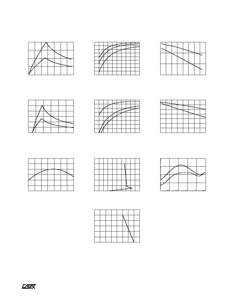
4
8
12
16
20
24
28
32
36
LINE INPUT (VOLTS)
0.0
0.2
0.4
0.6
0.8
INPUT CURRENT (AMPS)
24 VOLT INPUT CURRENT Vs. LINE INPUT VOLTAGE
100% LOAD
50% LOAD
0
10
20
30
40
50
60
70
80
90
100
LOAD (%)
60
65
70
75
80
85
90
EFFICIENCY (%)
24 VOLT EFFICIENCY Vs. LOAD
LINE =
18VDC
LINE =
24VDC
LINE =
36VDC
18
20
22
24
26
28
30
32
34
36
LINE INPUT(VOLTS)
80
82
84
86
88
EFFICIENCY(%)
24 VOLT EFFICIENCY Vs. LINE INPUT VOLTAGE
100% FULL LOAD
50% FULL LOAD
Data For 24 Volt Input Models
4
6
8
10
12
14
16
18
LINE INPUT (VOLTS)
0.0
0.5
1.0
1.5
INPUT CURRENT (AMPS)
12 VOLT INPUT CURRENT Vs. LINE INPUT VOLTAGE
100% LOAD
50% LOAD
0
10
20
30
40
50
60
70
80
90
100
LOAD (%)
65
70
75
80
85
EFFICIENCY (%)
12 VOLT EFFICIENCY Vs. LOAD
LINE =
9VDC
LINE =
12VDC
LINE =
18VDC
9
10
11
12
13
14
15
16
17
18
LINE INPUT(VOLTS)
80
81
82
83
84
85
EFFICIENCY(%)
12 VOLT EFFICIENCY Vs. LINE INPUT VOLTAGE
100% FULL LOAD
50% FULL LOAD
Data For 12 Volt Input Models
Typical Performance (Tc=25∞C, Vin=Nom VDC, Rated Load).
A
10 Watt NT Single Series DC/DC Converters
2401 Stanwell Drive ∑ Concord, California 94520 ∑ Ph: 925/687-4411 or 800/542-3355 ∑ Fax: 925/687-3333 ∑ www.calex.com ∑ Email: sales@calex.com
6
eco# 041007-1, 060831-1
Typical Performance (Tc=25∞C, Vin=Nom VDC, Rated Load).
Data For 48 Volt Input Models
5
15
25
35
45
55
65
75
LINE INPUT (VOLTS)
0.0
0.1
0.2
0.3
0.4
INPUT CURRENT (AMPS)
48 VOLT INPUT CURRENT Vs. LINE INPUT VOLTAGE
100% LOAD
50% LOAD
0
10
20
30
40
50
60
70
80
90
100
LOAD (%)
40
45
50
55
60
65
70
75
80
85
EFFICIENCY (%)
48 VOLT EFFICIENCY Vs. LOAD
LINE =
36VDC
LINE =
48VDC
LINE =
72VDC
35
40
45
50
55
60
65
70
75
LINE INPUT(VOLTS)
70
75
80
85
EFFICIENCY(%)
48 VOLT EFFICIENCY Vs. LINE INPUT VOLTAGE
100% FULL LOAD
50% FULL LOAD
Data For 48S5.1500NT Only
0
10
20
30
40
50
60
LINE INPUT (VOLTS)
0.0
0.1
0.2
0.3
0.4
0.5
0.6
INPUT CURRENT (AMPS)
INPUT CURRENT Vs. LINE INPUT VOLTAGE
100% LOAD
50% LOAD
0
10
20
30
40
50
60
70
80
90
100
LOAD (%)
45
50
55
60
65
70
75
80
85
EFFICIENCY (%)
EFFICIENCY Vs. LOAD
LINE = 20VDC
LINE = 48VDC
LINE = 60VDC
20
25
30
35
40
45
50
55
60
LINE INPUT(VOLTS)
50
55
60
65
70
75
80
85
EFFICIENCY(%)
48 VOLT EFFICIENCY Vs. LINE INPUT VOLTAGE
100% FULL LOAD
50% FULL LOAD
Data For All Models
-40
-20
0
20
40
60
80
100
CASE TEMPERATURE (Deg C)
-0.4
-0.3
-0.2
-0.1
0.0
0.1
0.2
NORMALIZED OUTPUT (%)
OUTPUT VOLTAGE Vs. CASE TEMPERATURE
0
20
40
60
80
100
120
140
160
180
200
OUTPUT LOAD (%)
0
20
40
60
80
100
120
NORMALIZED OUTPUT (%)
OUTPUT VOLTAGE Vs. OUTPUT LOAD
CURRENT LIMIT MODE ->
"HICKUP" MODE ->
10
100
1000
10000
100000
1000000
FREQUENCY (Hz)
.001
.01
.1
1
10
OUTPUT IMPEDANCE (OHMS)
OUTPUT IMPEDANCE Vs. FREQUENCY
3.3 AND 5 VOLT
12 AND 15 VOLT
NOTES ON USING THE CURVES
These notes apply to all curves except the 48S5.1500NT curves.
(1)
The input current curves are for 10.8 Watts of output power. For
3.3 Volt output models the input current is approximately 35%
less.
(2)
The efficiency curves were generated for 12 Volt output models.
To use for other outputs adjust as follows:
3.33 Volt output.......Subtract approximately 3%
5.0 Volt output........Subtract approximately 2%
15.0 Volt output.......Add approximately 1%
-40
-20
0
20
40
60
80
100
120
AMBIENT TEMPERATURE (Deg C)
0
20
40
60
80
100
120
OUTPUT POWER (%)
DERATING
INFINITE HEAT SINK
NO HEAT SINK
SAFE OPERATING AREA