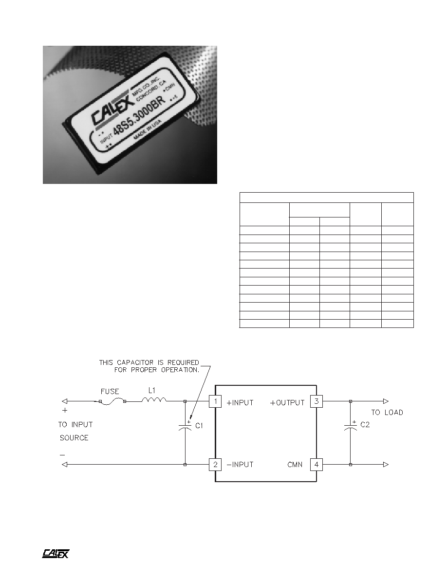
A
15 Watt BR Single Series DC/DC Converters
2401 Stanwell Drive ∑ Concord, California 94520 ∑ Ph: 925/687-4411 or 800/542-3355 ∑ Fax: 925/687-3333 ∑ www.calex.com ∑ Email: sales@calex.com
1
4/2001, eco# 010614-2, 020318-2, 020815-1, 030728-3, 041007-1, 060831-1
Features
Up to15 Watts of Output Power
Wide Input Range
Rated to 100∞C Case Operating Temperature
24 & 48 Volt Nominal Inputs,
1.8, 2.5, 3.3, 5, 12 and 15 Volt Outputs
Five Year Warranty
Water Washable Design
Description
The Calex BR series are 15 Watt DC/DC converters in a 1" x
2" case with a 4:1 input ratio. The input voltage range is 9 to
36 VDC for 24 Volt models and 18 to 72 for 48 Volt models.
The BR series requires a low source impedance at the input
terminals by using an external capacitor (see Application
Notes). These models do not have an internal input filter.
The units are filled with a compound which allows them to
withstand a normal water wash after being soldered to a PC
board.
t
r
a
h
C
n
o
i
t
c
e
l
e
S
l
e
d
o
M
e
g
n
a
R
t
u
p
n
I
C
D
V
t
u
p
t
u
O
C
D
V
t
u
p
t
u
O
A
m
n
i
M
x
a
M
R
B
0
0
5
4
.
8
R
1
S
4
2
9
6
3
8
.
1
0
0
5
4
R
B
0
0
5
4
.
5
R
2
S
4
2
9
6
3
5
.
2
0
0
5
4
R
B
0
0
5
4
.
3
R
3
S
4
2
9
6
3
3
.
3
0
0
5
4
R
B
0
0
0
3
.
5
S
4
2
9
6
3
5
0
0
0
3
R
B
0
5
2
1
.
2
1
S
4
2
9
6
3
2
1
0
5
2
1
R
B
0
0
0
1
.
5
1
S
4
2
9
6
3
5
1
0
0
0
1
R
B
0
0
5
4
.
8
R
1
S
8
4
8
1
*
2
7
8
.
1
0
0
5
4
R
B
0
0
5
4
.
5
R
2
S
8
4
8
1
*
2
7
5
.
2
0
0
5
4
R
B
0
0
5
4
.
3
R
3
S
8
4
8
1
*
2
7
3
.
3
0
0
5
4
R
B
0
0
0
3
.
5
S
8
4
8
1
*
2
7
5
0
0
0
3
R
B
0
5
2
1
.
2
1
S
8
4
8
1
*
2
7
2
1
0
5
2
1
R
B
0
0
0
1
.
5
1
S
8
4
8
1
*
2
7
5
1
0
0
0
1
Figure 1. Recommended application
*UL Recognition only applies up to 60VDC

A
15 Watt BR Single Series DC/DC Converters
2401 Stanwell Drive ∑ Concord, California 94520 ∑ Ph: 925/687-4411 or 800/542-3355 ∑ Fax: 925/687-3333 ∑ www.calex.com ∑ Email: sales@calex.com
2
4/2001, eco# 010614-2, 020318-2, 020815-1, 030728-3, 041007-1, 060831-1
NOTES:
(1)
Refer to the CALEX Application Notes for the definition of terms,
measurement circuits, and other information.
Load Transient Overshoot is the output voltage peak amplitude
referenced to the final value due to a step load change of 50-
75%. "Load Transient Overshoot" and "Dynamic Response" are
the same specification. Load Transient Recovery Time is the
time for the output to return to within the specified voltage error
band centered about the final value. "Load Transient Recovery
Time" and "Transient Response" are the same specification.
(2)
See CALEX Application Notes to determine the correct fuse. A
fuse is required only for system protection, but must be used for
reverse voltage protection of the input.
(3)
Below the minimum rated load, the output may exhibit noise
Electrical Characteristics
Unless otherwise specified, all parameters are full load, nominal line, T
A
=25∞C, and thermal steady state.
)
1
(
s
r
e
t
e
m
a
r
a
P
t
u
p
n
I
l
e
d
o
M
R
B
0
0
5
4
.
8
R
1
S
4
2
R
B
0
0
5
4
.
5
R
2
S
4
2
R
B
0
0
5
4
.
3
R
3
S
4
2
R
B
0
0
0
3
.
5
S
4
2
R
B
0
5
2
1
.
2
1
S
4
2
R
B
0
0
0
1
.
5
1
S
4
2
s
t
i
n
U
e
g
n
a
R
e
g
a
t
l
o
V
N
I
M
M
O
N
X
A
M
9
4
2
6
3
C
D
V
d
a
o
L
o
N
,
t
n
e
r
r
u
C
t
u
p
n
I
d
a
o
L
ll
u
F
P
Y
T
P
Y
T
0
1
3
7
4
0
1
0
3
6
0
1
0
8
7
0
1
3
5
7
0
1
4
4
7
0
1
4
4
7
C
D
A
m
y
c
n
e
i
c
i
f
f
E
d
a
o
L
ll
u
F
,
C
D
V
4
2
=
n
i
V
P
Y
T
2
7
5
7
0
8
3
8
4
8
4
8
%
y
c
n
e
u
q
e
r
F
g
n
i
h
c
t
i
w
S
P
Y
T
0
0
4
z
H
k
,
e
g
a
t
l
o
v
r
e
v
O
t
u
p
n
I
m
u
m
i
x
a
M
s
m
0
0
1
X
A
M
0
4
C
D
V
e
s
u
F
d
e
d
n
e
m
m
o
c
e
R
)
2
(
S
P
M
A
l
e
d
o
M
R
B
0
0
5
4
.
8
R
1
S
8
4
R
B
0
0
5
4
.
5
R
2
S
8
4
R
B
0
0
5
4
.
3
R
3
S
8
4
R
B
0
0
0
3
.
5
S
8
4
R
B
0
5
2
1
.
2
1
S
8
4
R
B
0
0
0
1
.
5
1
S
8
4
s
t
i
n
U
e
g
n
a
R
e
g
a
t
l
o
V
N
I
M
M
O
N
X
A
M
8
1
8
4
*
2
7
C
D
V
d
a
o
L
o
N
,
t
n
e
r
r
u
C
t
u
p
n
I
d
a
o
L
ll
u
F
P
Y
T
P
Y
T
0
1
6
3
2
0
1
0
2
3
0
1
5
8
3
0
1
7
7
3
0
1
2
7
3
0
1
2
7
3
C
D
A
m
y
c
n
e
i
c
i
f
f
E
d
a
o
L
ll
u
F
,
C
D
V
8
4
=
n
i
V
P
Y
T
2
7
5
7
0
8
3
8
4
8
4
8
%
y
c
n
e
u
q
e
r
F
g
n
i
h
c
t
i
w
S
P
Y
T
0
0
4
z
H
k
,
e
g
a
t
l
o
v
r
e
v
O
t
u
p
n
I
m
u
m
i
x
a
M
s
m
0
0
1
X
A
M
0
8
C
D
V
e
s
u
F
d
e
d
n
e
m
m
o
c
e
R
)
2
(
S
P
M
A
)
1
(
s
r
e
t
e
m
a
r
a
P
t
u
p
t
u
O
l
e
d
o
M
R
B
0
0
5
4
.
8
R
1
S
4
2
R
B
0
0
5
4
.
8
R
1
S
8
4
R
B
0
0
5
4
.
5
R
2
S
4
2
R
B
0
0
5
4
.
5
R
2
S
8
4
R
B
0
0
5
4
.
3
R
3
S
4
2
R
B
0
0
5
4
.
3
R
3
S
8
4
R
B
0
0
0
3
.
5
S
4
2
R
B
0
0
0
3
.
5
S
8
4
R
B
0
5
2
1
.
2
1
S
4
2
R
B
0
5
2
1
.
2
1
S
8
4
R
B
0
0
0
1
.
5
1
S
4
2
R
B
0
0
0
1
.
5
1
S
8
4
s
t
i
n
U
e
g
a
t
l
o
V
t
u
p
t
u
O
8
.
1
5
.
2
3
.
3
5
2
1
5
1
C
D
V
e
g
a
t
l
o
V
t
u
p
t
u
O
y
c
a
r
u
c
c
A
N
I
M
P
Y
T
X
A
M
0
5
7
.
1
0
0
8
.
1
0
5
8
.
1
0
5
4
.
2
0
0
5
.
2
0
5
5
.
2
4
3
2
.
3
0
0
3
.
3
6
6
3
.
3
0
9
.
4
0
0
.
5
0
1
.
5
6
7
.
1
1
0
0
.
2
1
4
2
.
2
1
0
7
.
4
1
0
0
.
5
1
0
3
.
5
1
C
D
V
)
3
(
e
g
n
a
R
d
a
o
L
d
e
t
a
R
N
I
M
X
A
M
8
6
.
0
4
5
.
4
8
6
.
0
4
5
.
4
8
6
.
0
4
5
.
4
5
4
.
0
0
0
.
3
9
1
.
0
5
2
.
1
5
1
.
0
0
0
.
1
C
D
A
n
o
i
t
a
l
u
g
e
R
d
a
o
L
L
F
-
L
F
4
/
1
P
Y
T
X
A
M
1
.
0
1
%
n
o
i
t
a
l
u
g
e
R
e
n
i
L
C
D
V
x
a
M
-
n
i
M
=
n
i
V
P
Y
T
X
A
M
2
0
.
0
2
.
0
2
0
.
0
1
.
0
%
t
o
o
h
s
r
e
v
O
n
O
r
e
w
o
P
P
Y
T
5
.
0
V
t
n
e
i
s
n
a
r
T
d
a
o
L
)
1
(
e
m
i
T
y
r
e
v
o
c
e
R
%
1
±
=
d
n
a
b
r
o
r
r
e
P
Y
T
0
0
2
s
µ
t
n
e
i
s
n
a
r
T
d
a
o
L
t
o
o
h
s
r
e
v
O
P
Y
T
0
5
1
0
0
3
V
m
k
a
e
p
)
4
(
e
s
i
o
N
z
H
M
1
-
1
0
.
0
=
w
b
z
H
M
0
2
-
0
=
w
b
P
Y
T
P
Y
T
0
0
1
0
5
1
P
-
P
V
m
t
n
e
i
c
i
f
f
e
o
C
e
r
u
t
a
r
e
p
m
e
T
P
Y
T
X
A
M
0
5
0
5
1
C
∞
/
m
p
p
,
n
o
i
t
c
e
t
o
r
P
t
i
u
c
r
i
C
t
r
o
h
S
n
o
m
m
o
C
o
t
t
u
p
t
u
O
s
u
o
u
n
i
t
n
o
C
performance degradation. Operation with less than the minimum
rated load will not damage unit, and DC regulation is not
significantly affected.
(4)
Noise is measured per CALEX Application Notes. Output noise
is measured with a 10 µF tantalum capacitor and a 0.01µF
ceramic capacitor connected across the output pins.
(5)
The Case is tied to the -input pin.
(6)
The case thermal impedance is specified as the case temperature
rise over ambient per package watt dissipated.
(7)
Specifications subject to change without notice.
(8)
Water Washability - Calex DC/DC converters are designed to
withstand most solder/wash processes. Careful attention should
be used when assessing the applicability in your specific
manufacturing process. Converters are not hermetically sealed.
*UL Recognition only applies up to 60VDC
A
15 Watt BR Single Series DC/DC Converters
2401 Stanwell Drive ∑ Concord, California 94520 ∑ Ph: 925/687-4411 or 800/542-3355 ∑ Fax: 925/687-3333 ∑ www.calex.com ∑ Email: sales@calex.com
3
4/2001, eco# 010614-2, 020318-2, 020815-1, 030728-3, 041007-1, 060831-1
s
n
o
i
t
a
c
i
f
i
c
e
p
S
l
a
r
e
n
e
G
s
l
e
d
o
M
l
l
A
s
t
i
n
U
)
5
(
n
o
i
t
a
l
o
s
I
e
g
a
t
l
o
V
n
o
i
t
a
l
o
s
I
S
4
2
t
u
p
t
u
O
o
t
t
u
p
n
I
S
8
4
t
u
p
t
u
O
o
t
t
u
p
n
I
N
I
M
N
I
M
0
0
7
0
0
5
1
C
D
V
t
u
p
t
u
O
o
t
t
u
p
n
I
e
c
n
a
t
i
c
a
p
a
C
P
Y
T
0
0
6
1
F
p
l
a
t
n
e
m
n
o
r
i
v
n
E
e
g
n
a
R
g
n
i
t
a
r
e
p
O
e
s
a
C
N
I
M
X
A
M
0
4
-
0
0
1
C
∞
e
g
n
a
R
e
g
a
r
o
t
S
N
I
M
X
A
M
5
5
-
5
2
1
C
∞
)
6
(
e
c
n
a
d
e
p
m
I
l
a
m
r
e
h
T
P
Y
T
5
1
t
t
a
W
/
C
∞
l
a
r
e
n
e
G
t
h
g
i
e
W
t
i
n
U
P
Y
T
1
.
1
z
o
t
i
K
g
n
i
t
n
u
o
M
s
i
s
s
a
h
C
8
S
M
F
B
T
M
s
r
u
o
H
M
1
>
s
l
a
v
o
r
p
p
A
y
c
n
e
g
A
0
5
9
0
6
L
U
/
A
S
C
Application Notes
General
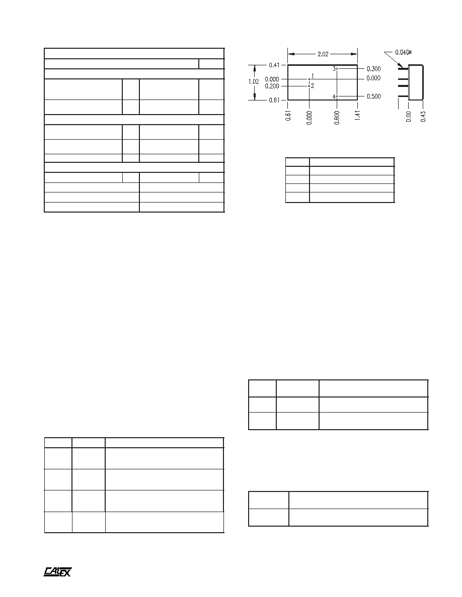
Figure 1 shows the recommended connections for the 15 Watt
BR Single. Capacitor C1 is mandatory for proper operation as
the BR may be damaged if operated without it. C1 must be
rated to handle the ripple current from the BR input. L1 is
optional and serves to reduce the reflected ripple current from
the BR back into the Input Source. L1 must be rated to handle
the DC input current. Information about C1 and L1 is shown
in the following paragraphs. The fuse is required only for
system protection (Note 2).
Capacitor C2 is optional and serves to further reduce
output noise. It may be made up of several capacitors already
in your system that are distributed at the loads.
:
s
'
N
/
P
r
o
t
i
c
a
p
a
C
d
e
t
s
e
g
g
u
S
l
e
d
o
M
e
p
y
T
N
/
P
S
4
2
e
l
o
h
u
r
h
T
C
∞
5
8
+
t
a
A
0
.
2
,
s
m
h
o
9
5
0
.
0
,
V
0
5
,
F
µ
0
7
4
)
C
∞
5
0
1
+
t
a
A
2
.
1
(
0
2
X
5
.
2
1
V
0
5
M
1
7
4
Z
S
R
N
:
C
I
N
S
4
2
T
M
S
e
s
U
.
C
∞
5
8
+
t
a
A
9
4
.
0
,
s
m
h
o
6
.
0
,
V
0
5
,
F
µ
8
.
6
.
l
e
ll
a
r
a
p
n
i
4
2
D
0
5
0
9
X
5
8
6
D
3
9
5
:
e
u
g
a
r
p
S
y
a
h
s
i
V
S
8
4
e
l
o
h
u
r
h
T
C
∞
5
8
+
t
a
A
0
.
1
,
s
m
h
o
4
2
.
0
,
V
0
0
1
,
F
µ
8
6
)
C
∞
5
0
1
+
t
a
A
3
6
.
0
(
0
2
X
0
1
V
0
0
1
M
0
8
6
Z
S
R
N
:
C
I
N
S
8
4
T
M
S
C
∞
5
8
+
t
a
A
1
.
1
,
s
m
h
o
7
1
.
0
,
V
0
0
1
,
F
µ
0
0
1
)
C
∞
5
0
1
+
t
a
A
9
7
.
0
(
7
1
X
6
1
V
0
0
1
M
1
0
1
K
C
A
N
:
C
I
N
.
z
H
k
0
0
1
t
a
e
r
a
s
g
n
i
t
a
r
R
S
E
d
n
a
t
n
e
r
r
u
c
e
l
p
p
i
r
e
h
T
.
s
r
e
r
u
t
c
a
f
u
n
a
m
r
e
h
t
o
m
o
r
f
e
l
b
a
l
i
a
v
a
e
r
a
s
t
n
e
l
a
v
i
u
q
E
:
s
t
n
e
m
e
r
i
u
q
e
R
1
C
l
e
d
o
M
e
g
a
t
l
o
V
t
u
p
n
I
C
D
V
t
n
e
r
r
u
C
e
l
p
p
i
R
r
o
t
i
c
a
p
a
C
d
e
r
i
u
q
e
R
g
n
i
t
a
r
m
u
m
i
n
i
m
,
S
M
R
-
A
S
4
2
6
3
o
t
9
8
.
1
S
8
4
2
7
o
t
8
1
9
.
0
:
s
'
N
/
P
r
o
t
c
u
d
n
I
d
e
t
s
e
g
g
u
S
e
l
o
h
u
r
h
T
.
s
m
h
o
0
3
0
.
0
,
C
D
A
2
.
4
,
H
µ
0
1
0
0
1
-
0
1
0
8
0
B
F
R
:
t
f
a
r
c
l
i
o
C
T
M
S
.
s
m
h
o
0
4
0
.
0
,
C
D
A
5
.
3
,
H
µ
0
1
3
0
1
-
P
0
4
3
3
O
D
:
t
f
a
r
c
l
i
o
C
.
s
r
e
r
u
t
c
a
f
u
n
a
m
r
e
h
t
o
m
o
r
f
e
l
b
a
l
i
a
v
a
e
r
a
s
t
n
e
l
a
v
i
u
q
E
Input Capacitor
C1 in figure 1 is mandatory and must be connected across the
input pins for proper operation. Locate C1 within 1" maximum
from the input pins.
Input Inductor
The same inductor is suitable for both 24S and 48S models of
the BR.
The following table lists the requirements for C1
Mechanical tolerances unless otherwise noted:
X.XX dimensions: ±0.020 inches
X.XXX dimensions: ±0.005 inches
Pin location is for the matiing PCB.
The case is metal with a non-conductive header
BOTTOM VIEW
SIDE VIEW
n
i
P
n
o
i
t
c
n
u
F
1
T
U
P
N
I
+
2
E
S
A
C
,
T
U
P
N
I
-
3
T
U
P
T
U
O
+
4
N
M
C
±0.002
0.3 TYP
Note: On nominal 48Vin Models UL Recognition only applies
up to 60VDC.

A
15 Watt BR Single Series DC/DC Converters
2401 Stanwell Drive ∑ Concord, California 94520 ∑ Ph: 925/687-4411 or 800/542-3355 ∑ Fax: 925/687-3333 ∑ www.calex.com ∑ Email: sales@calex.com
4
4/2001, eco# 010614-2, 020318-2, 020815-1, 030728-3, 041007-1, 060831-1
:
r
e
t
l
i
F
t
u
p
n
I
:
s
t
l
u
s
e
r
g
n
i
w
o
ll
o
f
e
h
t
s
e
v
i
g
n
w
o
h
s
s
e
u
l
a
v
e
h
t
h
t
i
w
r
e
t
l
i
f
t
u
p
n
i
n
a
g
n
i
s
U
l
e
d
o
M
1
C
1
L
t
n
e
r
r
u
C
e
l
p
p
i
R
d
e
t
c
e
l
f
e
R
S
4
2
r
u
o
F
m
u
l
a
t
n
a
T
V
0
5
/
F
µ
8
.
6
H
µ
0
1
P
-
P
A
m
0
5
t
u
o
b
A
S
M
R
A
m
0
2
t
u
o
b
A
S
8
4
V
0
0
1
/
F
µ
0
0
1
H
µ
0
1
P
-
P
A
m
5
2
t
u
o
b
A
S
M
R
A
m
2
1
t
u
o
b
A
.
e
k
i
p
s
g
n
i
h
c
t
i
w
s
e
h
t
e
d
u
l
c
n
i
t
o
n
s
e
o
d
t
n
e
r
r
u
C
d
e
t
c
e
l
f
e
R
P
-
P
The C1 and L1 parts listed above are suitable for the BR
operating at full power output. These C1 and L1 parts will work
up to +85∞C ambient temperture, although the BR itself will
require some sort of heatsink or cooling to operate at full
power at +85∞C ambient. More filtering can be accomplished
by increasing the value of C1 and lowering its ESR which is
done by paralleling capacitors. In addition adding an optional
ceramic capacitor of 0.1 to 1.0µF close to the pins will further
help reduce the spike.
Increasing the value of L1 requires at least a proportional
increase in the value of C1. i.e. If L1 is doubled then at least
double the value of C1 shown in the table. Not using L1 (but
MUST have C1) will increase the Reflected Ripple Current
back into the the Input Source power supply.
Measurement Technique
Using the ground clip lead on a scope probe will show sharp
switching spikes on the oscilloscope, while using a tip jack will
minimize this effect. There will generally be a switching spike
when scoping the input pins which happens because capacitor
C1 cannot be located directly on the BR input pins.