 | –≠–ª–µ–∫—Ç—Ä–æ–Ω–Ω—ã–π –∫–æ–º–ø–æ–Ω–µ–Ω—Ç: 48S5.8XT | –°–∫–∞—á–∞—Ç—å:  PDF PDF  ZIP ZIP |

A
45 Watt XT Single Series DC/DC Converters
2401 Stanwell Drive ∑ Concord, California 94520 ∑ Ph: 925/687-4411 or 800/542-3355 ∑ Fax: 925/687-3333 ∑ www.calex.com ∑ Email: sales@calex.com
1
eco# 041007-1, eco# 050317-3, eco# 050929-4
Features
Fully Shielded/Filtered Design
Lowest Noise Outputs, 50 mV P-P
Very Low and Specified Reflected Ripple Current
Low I/O Capacitance, 500 pF Typical
Water Washable Shielded Copper Case
Five Year Warranty
Description
These single output converters are designed for ultra wide
input range low noise telecommunications, industrial, and
instrument applications. The very wide input range (4:1) is
ideal for battery or unregulated input applications while the
low noise complements even the most sensitive analog
circuitry.
These converters are state of the art 220 kHz MOSFET
based designs that provide outstanding line and load regulation
and efficiencies exceeding 80%.
Remote output voltage sense, output voltage trim and ON/
OFF functions are also included.
The converters are protected from output shorts to common
by a high speed pulse by pulse digital current limit circuit and
a self resetting thermal overload protection circuit.
As with all CALEX converters the 45 watt XT Single series
is covered by our 5 Year Warranty.
45 Watt XT Single Series Block Diagram
t
r
a
h
C
n
o
i
t
c
e
l
e
S
l
e
d
o
M
e
g
n
a
R
t
u
p
n
I
C
D
V
t
u
p
t
u
O
C
D
V
t
u
p
t
u
O
S
P
M
A
n
i
M
x
a
M
T
X
6
.
3
S
4
2
9
6
3
3
3
.
3
0
.
6
T
X
7
.
5
S
4
2
9
6
3
0
.
5
0
.
7
T
X
4
.
2
1
S
4
2
9
6
3
0
.
2
1
5
7
.
3
T
X
3
.
5
1
S
4
2
9
6
3
0
.
5
1
0
.
3
T
X
7
.
3
S
8
4
0
2
2
7
3
3
.
3
0
.
7
T
X
8
.
5
S
8
4
*
0
2
2
7
0
.
5
0
.
8
T
X
4
.
2
1
S
8
4
0
2
2
7
0
.
2
1
5
7
.
3
T
X
3
.
5
1
S
8
4
0
2
2
7
0
.
5
1
0
.
3
.
s
l
e
d
o
M
S
4
2
r
o
f
s
e
v
r
u
C
g
n
i
t
a
r
e
D
t
u
p
n
I
e
e
S
:
e
t
o
N
0
5
9
0
6
L
U
/
A
S
C
:
s
l
a
v
o
r
p
p
A
y
c
n
e
g
A
*

A
45 Watt XT Single Series DC/DC Converters
2401 Stanwell Drive ∑ Concord, California 94520 ∑ Ph: 925/687-4411 or 800/542-3355 ∑ Fax: 925/687-3333 ∑ www.calex.com ∑ Email: sales@calex.com
2
eco# 041007-1, eco# 050317-3, eco# 050929-4
NOTES
*
All parameters measured at Tc = 25∞C, nominal input voltage
and full rated load unless otherwise noted. Refer to the
CALEX Application Notes for the definition of terms,
measurement circuits and other information.
(1)
Noise is measured per CALEX application notes. Measurement
bandwidth is 0-20 MHz. RMS noise is measured over a 0.01-1
MHz bandwidth. To simulate standard PCB decoupling practices,
output noise is measured with a 10µf tantalum and 0.01µF
ceramic capacitor located 1 inch away from the converter. Input
ripple is measured into a 10µH source impedance.
(2)
See our application note for picking the correct fuse size.
(3)
Transient response is specified for a 50 to 75% step load
change. Rise time of step is 2 microseconds.
(4)
Dynamic response is the peak overshoot for a transient as
described in note 3.
(5)
Input ripple rejection is specified for a DC to 120 Hz ripple with
a modulation amplitude of 1% of Vin or less.
(6)
The functional temperature range is intended to give an additional
data point for use in evaluating this power supply. At the
low functional temperature the power supply will function with
no side effects, however sustained operation at the high
functional temperature may reduce the expected operational
life. The data sheet specifications are not guaranteed over
the functional temperature range.
(7)
The case thermal impedance is specified as the case temperature
rise over ambient per package watt dissipated.
*
s
r
e
t
e
m
a
r
a
P
t
u
p
n
I
l
e
d
o
M
T
X
6
.
3
S
4
2
T
X
7
.
5
S
4
2
T
X
4
.
2
1
S
4
2
T
X
3
.
5
1
S
4
2
s
t
i
n
U
)
8
(
e
g
n
a
R
e
g
a
t
l
o
V
N
I
M
X
A
M
9
6
3
C
D
V
d
a
o
L
ll
u
F
t
n
e
r
r
u
C
t
u
p
n
I
d
a
o
L
o
N
P
Y
T
P
Y
T
0
2
1
1
0
1
0
0
9
1
0
1
0
0
4
2
0
1
0
0
4
2
0
1
A
m
y
c
n
e
i
c
i
f
f
E
P
Y
T
4
7
6
7
9
7
9
7
%
)
1
(
e
l
p
p
i
R
d
e
t
c
e
l
f
e
R
P
Y
T
0
6
p
-
p
A
m
P
Y
T
8
S
M
R
A
m
y
c
n
e
u
q
e
r
F
g
n
i
h
c
t
i
w
S
P
Y
T
0
2
2
z
H
k
s
m
0
0
1
,
e
g
a
t
l
o
v
r
e
v
O
t
u
p
n
I
m
u
m
i
x
a
M
X
A
M
5
4
C
D
V
r
o
r
r
E
t
u
p
t
u
O
%
1
,
e
m
i
T
n
o
-
n
r
u
T
P
Y
T
5
2
s
m
e
s
u
F
d
e
d
n
e
m
m
o
c
e
R
)
2
(
S
P
M
A
l
e
d
o
M
T
X
7
.
3
S
8
4
T
X
8
.
5
S
8
4
T
X
4
.
2
1
S
8
4
T
X
3
.
5
1
S
8
4
s
t
i
n
U
e
g
n
a
R
e
g
a
t
l
o
V
N
I
M
X
A
M
0
2
2
7
C
D
V
d
a
o
L
ll
u
F
t
n
e
r
r
u
C
t
u
p
n
I
d
a
o
L
o
N
P
Y
T
P
Y
T
0
4
6
0
1
0
5
0
1
0
1
0
5
1
1
0
1
0
5
1
1
0
1
A
m
y
c
n
e
i
c
i
f
f
E
P
Y
T
6
7
9
7
1
8
1
8
%
)
1
(
e
l
p
p
i
R
d
e
t
c
e
l
f
e
R
P
Y
T
5
4
p
-
p
A
m
P
Y
T
5
S
M
R
A
m
y
c
n
e
u
q
e
r
F
g
n
i
h
c
t
i
w
S
P
Y
T
0
2
2
z
H
k
s
m
0
0
1
,
e
g
a
t
l
o
v
r
e
v
O
t
u
p
n
I
m
u
m
i
x
a
M
X
A
M
0
8
C
D
V
r
o
r
r
E
t
u
p
t
u
O
%
1
,
e
m
i
T
n
o
-
n
r
u
T
P
Y
T
5
2
s
m
e
s
u
F
d
e
d
n
e
m
m
o
c
e
R
)
2
(
S
P
M
A
*
s
r
e
t
e
m
a
r
a
P
t
u
p
t
u
O
l
e
d
o
M
T
X
6
.
3
S
4
2
T
X
7
.
3
S
8
4
T
X
7
.
5
S
4
2
T
X
8
.
5
S
8
4
T
X
4
.
2
1
S
4
2
T
X
4
.
2
1
S
8
4
T
X
3
.
5
1
S
4
2
T
X
3
.
5
1
S
8
4
S
T
I
N
U
e
g
a
t
l
o
V
t
u
p
t
u
O
3
3
.
3
5
2
1
5
1
C
D
V
y
c
a
r
u
c
c
A
e
g
a
t
l
o
V
t
u
p
t
u
O
N
I
M
P
Y
T
X
A
M
0
3
.
3
3
3
.
3
6
3
.
3
5
9
.
4
0
0
.
5
5
0
.
5
0
9
.
1
1
0
0
.
2
1
0
1
.
2
1
0
9
.
4
1
0
0
.
5
1
0
1
.
5
1
C
D
V
)
9
(
e
g
n
a
R
d
a
o
L
d
e
t
a
R
N
I
M
X
A
M
5
.
1
6
5
.
1
7
7
.
1
7
3
.
0
8
3
.
0
5
7
.
3
3
.
0
3
A
%
0
0
1
-
%
5
2
:
n
o
i
t
a
l
u
g
e
R
d
a
o
L
d
a
o
L
ll
u
F
P
Y
T
1
.
0
%
n
o
i
t
a
l
u
g
e
R
e
n
i
L
)
2
1
,
8
(
C
D
V
x
a
M
-
n
i
M
=
n
i
V
P
Y
T
X
A
M
5
.
0
0
.
2
1
.
0
2
.
0
%
)
3
(
e
s
n
o
p
s
e
R
t
n
e
i
s
n
a
r
T
P
Y
T
0
0
5
0
0
1
0
0
1
0
0
1
s
µ
)
4
(
e
s
n
o
p
s
e
R
c
i
m
a
n
y
D
P
Y
T
0
0
2
0
5
2
0
2
1
0
2
1
k
a
e
p
V
m
)
5
(
n
o
i
t
c
e
j
e
R
e
l
p
p
i
R
t
u
p
n
I
P
Y
T
5
2
>
B
d
)
1
(
w
b
z
H
M
0
2
-
0
,
e
s
i
o
N
P
Y
T
5
2
5
2
5
2
0
5
5
2
0
5
5
2
0
5
p
-
p
V
m
)
1
(
w
b
z
H
M
1
-
1
.
0
,
e
s
i
o
N
S
M
R
P
Y
T
6
0
1
6
0
1
6
0
1
6
0
1
S
M
R
V
m
t
n
e
i
c
i
f
f
e
o
C
e
r
u
t
a
r
e
p
m
e
T
P
Y
T
X
A
M
0
5
0
5
1
C
∞
/
m
p
p
n
o
i
t
c
e
t
o
r
P
t
i
u
c
r
i
C
t
r
o
h
S
n
o
i
t
c
e
t
o
r
P
l
a
m
r
e
h
T
d
n
a
n
o
m
m
o
C
o
t
t
u
p
t
u
O

A
45 Watt XT Single Series DC/DC Converters
2401 Stanwell Drive ∑ Concord, California 94520 ∑ Ph: 925/687-4411 or 800/542-3355 ∑ Fax: 925/687-3333 ∑ www.calex.com ∑ Email: sales@calex.com
3
eco# 041007-1, eco# 050317-3, eco# 050929-4
n
i
P
n
o
i
t
c
n
u
F
1
T
U
P
N
I
+
2
T
U
P
N
I
-
3
E
S
N
E
S
+
4
M
I
R
T
5
E
S
N
E
S
-
6
T
U
P
T
U
O
+
7
N
M
C
8
F
F
O
/
N
O
Mechanical tolerances unless otherwise noted:
X.XX dimensions: ±0.020 inches
X.XXX dimensions: ±0.005 inches
Application Information
You truly get what you pay for in a CALEX converter, a
complete system oriented and specified DC/DC converter -
no surprises, no external noise filtering circuits needed, no
heatsinking problems, just "plug and play".
The 45 watt XT Single series like all CALEX converters
carries the full 5 year CALEX no hassle warranty. We can offer
a five year warranty where others can't because with CALEX
it's rarely needed.
Keep reading, you'll find out why.
*
s
n
o
i
t
a
c
i
f
i
c
e
p
S
l
a
r
e
n
e
G
s
l
e
d
o
M
l
l
A
s
t
i
n
U
n
o
i
t
c
n
u
F
F
F
O
/
N
O
l
e
v
e
L
c
i
g
o
L
N
O
n
e
p
O
n
i
P
e
v
a
e
L
r
o
N
I
M
4
C
D
V
l
e
v
e
L
c
i
g
o
L
F
F
O
t
u
p
n
I
-
o
t
n
i
P
e
i
T
r
o
X
A
M
5
.
1
C
D
V
e
g
a
t
l
o
V
t
i
u
c
r
i
C
n
e
p
O
P
Y
T
5
C
D
V
e
c
n
a
t
s
i
s
e
R
t
u
p
n
I
P
Y
T
6
s
m
h
o
k
t
n
e
r
r
u
C
e
l
d
I
r
e
t
r
e
v
n
o
C
w
o
L
n
i
P
F
F
O
/
N
O
P
Y
T
7
A
m
n
o
i
t
a
l
o
s
I
e
g
a
t
l
o
V
n
o
i
t
a
l
o
s
I
S
4
2
,
t
u
p
t
u
O
o
t
t
u
p
n
I
V
8
4
,
t
u
p
t
u
O
o
t
t
u
p
n
I
e
g
a
k
a
e
L
A
µ
0
1
N
I
M
N
I
M
0
0
7
4
4
5
1
C
D
V
t
u
p
t
u
O
o
t
t
u
p
n
I
e
c
n
a
t
i
c
a
p
a
C
P
Y
T
0
0
5
F
p
n
o
i
t
c
n
u
F
m
i
r
T
t
u
p
t
u
O
e
g
n
a
R
m
i
r
T
N
I
M
0
1
±
%
e
c
n
a
t
s
i
s
e
R
t
u
p
n
I
N
I
M
0
1
s
m
h
o
k
e
g
a
t
l
o
V
t
i
u
c
r
i
C
n
e
p
O
P
Y
T
5
.
2
C
D
V
l
a
t
n
e
m
n
o
r
i
v
n
E
e
g
n
a
R
g
n
i
t
a
r
e
p
O
e
s
a
C
N
I
M
X
A
M
0
4
-
5
8
C
∞
)
6
(
e
g
n
a
R
l
a
n
o
i
t
c
n
u
F
e
s
a
C
N
I
M
X
A
M
5
5
-
0
9
C
∞
e
g
n
a
R
e
g
a
r
o
t
S
N
I
M
X
A
M
5
5
-
0
0
1
C
∞
n
w
o
d
t
u
h
S
l
a
m
r
e
h
T
e
r
u
t
a
r
e
p
m
e
T
e
s
a
C
P
Y
T
0
0
1
C
∞
)
7
(
e
c
n
a
d
e
p
m
I
l
a
m
r
e
h
T
P
Y
T
4
.
4
t
t
a
W
/
C
∞
t
h
g
i
e
W
t
i
n
U
P
Y
T
7
z
o
s
n
o
i
t
p
O
g
n
i
t
n
u
o
M
9
S
M
t
i
K
g
n
i
t
n
u
o
M
s
i
s
s
a
h
C
r
e
b
m
u
N
t
r
a
P
n
o
x
i
f
f
u
S
I
-
e
s
a
C
n
I
s
t
r
e
s
n
I
r
e
b
m
u
N
t
r
a
P
n
o
x
i
f
f
u
S
S
H
-
n
o
i
t
p
O
k
n
i
S
t
a
e
H
BOTTOM VIEW
SIDE VIEW
General Information
The XT Single series is mindful of battery operation for
industrial, medical control and remote data collection
applications. The remote ON/OFF pin places the converter in
a very low power mode that draws typically less than 10 mA
from the input source.
Noise has also achieved new lows in this single design,
while the industry standard is to specify output noise as 1 to
5% peak to peak typical with no mention of measurement
bandwidth. The XT converters achieve 50 mV peak to peak
typical and are fully specified and tested to a wide bandwidth
of 0-20 MHz.
Input filtering reduces reflected ripple noise and is similarly
low and also fully specified for typical values (exact value
depends on input voltage range). Typical RMS noise over a 10
kHz to 1 MHz bandwidth is specified for both the input and
output.
Full overload protection is provided by independent pulse-
by-pulse current limiting and an over-temperature shutdown
circuit. These protection features assure you that our XT
single will provide you with zero failure rate operation.
Five sided shielding is standard along with specified operation
over the full industrial temperature range of -40 to +85∞C case
temperature.
(8)
See power/voltage derating curves.
(9)
No harm when operated at less than maximum load. See section
on Operation with Light Loads.
(10) Specifications subject to change without notice.
(11) Water Washability - Calex DC/DC converters are designed to
withstand most solder/wash processes. Careful attention should
be used when assessing the applicability in your specific
manufacturing process. Converters are not hermetically sealed.
(12) Line regulation for 12V and 15V models to be measured per
derating curve on page 7.
NOTES (cont)

A
45 Watt XT Single Series DC/DC Converters
2401 Stanwell Drive ∑ Concord, California 94520 ∑ Ph: 925/687-4411 or 800/542-3355 ∑ Fax: 925/687-3333 ∑ www.calex.com ∑ Email: sales@calex.com
4
eco# 041007-1, eco# 050317-3, eco# 050929-4
Applying the Input
Figure 1 shows the recommended input connections for the
XT Single DC/DC converter. A fuse is recommended to
protect the input circuit and should not be omitted. The fuse
serves to prevent unlimited current from flowing in the case of
a catastrophic system failure.
Figure 1.
Standard connections for the XT single input. The ON/OFF pin may
be left floating if it is not used. The input protection fuse should not
be omitted. If desired, an external transient protection diode (D1)
can be used at the input. See "Applying the input" for suggestions
regarding C1.
No external capacitance on the input is required for normal
operation, in fact it can degrade the converters performance.
Extremely low ESR capacitors (< 0.5 ohms) should not be
used at the input as this will cause peaking of the input filters
transfer function and actually degrade the filters performance.
Normal RF bypass capacitors in the 1000 pF to 0.01 µF range
may be used without harm.
Remote ON/OFF Pin Operation
The remote ON/OFF pin may be left floating if this function is
not used. The equivalent input circuit for the ON/OFF pin is
shown in figure 2. The best way to drive this pin is with an open
collector/drain or relay contact. See our application note titled
"Understanding the remote ON/OFF function" for more
information about using the remote ON/OFF pin.
When the ON/OFF pin is pulled low with respect to the -
Input, the converter is placed in a low power drain state. The
ON/OFF pin turns the converter off while keeping the input
bulk capacitor fully charged, this prevents the large inrush
current spike that occurs when the +input pin is opened and
closed.
Figure 2.
The simplified schematic of the XT Single series ON/OFF pin. The
input impedance is approximately 6k ohms. By leaving this pin
floating the converter will be in the ON state. When the pin is pulled
below 1.4 volts (with respect to the -Input pin) the converter is placed
in the power down or OFF state. See our application note on the
remote ON/OFF function for more information.
Applying The Output
Figure 3 shows typical output connections for the XT single.
In most applications no external output capacitance will be
necessarily. Only your normal 1 to 10 µF and 0.001 to 0.1 µF
bypass capacitors sprinkled around your circuit as needed
locally are required. Do not add extra output capacitance and
cost to your circuit "Just Because".
If you feel you must add external output capacitance, do
not use the lowest ESR, biggest value capacitor that you can
find! This can only lead to reduced system performance or
oscillation. See our application note "Understanding Output
Impedance For Optimum Decoupling" for more information.
Figure 3.
The remote sense lines should be connected to their respective
output pins even if they are not used in your application. If desired,
an external transient protection diode can be used. D2 and D3 are
optional, for more information see the "Remote sense" section.

A
45 Watt XT Single Series DC/DC Converters
2401 Stanwell Drive ∑ Concord, California 94520 ∑ Ph: 925/687-4411 or 800/542-3355 ∑ Fax: 925/687-3333 ∑ www.calex.com ∑ Email: sales@calex.com
5
eco# 041007-1, eco# 050317-3, eco# 050929-4
C1, C3 - 220µF, 25V UNITED CHEM-CON LXF SERIES
C2 - 0.01µF, 100V CERAMIC
L1 - 5µH POWER INDUCTOR
Remote Sense
The XT single features provisions for remote sense
connections. These allow the power supply to correct for line
drops of up to 0.6 volts per side. The remote sense connections
should be made with twisted pair wire or closely coupled PCB
traces. If the remote sense is not to be used these pins must
be connected to their respective output pins for proper output
voltage accuracy and regulation. There is approximately 2 mA
of current flowing in the remote sense lines.
Care should be taken to not disconnect the output pins
before the remote sense pins while the converter is in operation.
If this happens the output load current will run down the sense
leads possibly causing an output overvoltage condition. If the
unit must be "Hot Plugged" in the intended application, provision
should be made to disconnect the sense leads before the
power leads, disconnect the input power first or use the
remote ON/OFF to stop the converters operation.
Another option is to attach two 1N4001 diodes from pins 6
to 3 and pins 7 to 5 as shown in figure 3. These diodes will
shunt any current through the 10 ohm internal resistors
connected between the outputs and their respective outputs
when the voltage drop across the resistors exceeds
approximately 0.6 volts. This will limit momentary overvoltages
to about 1.2 volts during a hot plug-in.
Output Trimming
The trim pin may be used to adjust the outputs by up to ±10
% from the nominal factory setting. The trim may be used to
adjust for system wiring voltage drops or to adjust the +5
output up to 5.2 volts for ECL applications. Figure 4 shows the
proper connections to use the trim pin. If output trimming is not
desired the trim pin may be safely left floating.
Trimming the output up reduces the output current
proportionally to keep the maximum power constant. Output
current is not increased over the listed maximum when
trimming the output voltage down.
Figure 4.
The output can be trimmed by either a trimpot or fixed resistors. If
fixed resistors are used their values may range from 0 to infinite
ohms. The trimpot should be 10k ohms for 3.3 and 5 volt outputs or
20k ohms for 12 and 15 volt outputs.
Non Standard Output Voltages
The 12 and 15 volt XT's will typically trim much lower than the
-10% specified. This allows the 12 and 15 volt XT's to be
trimmed lower than specified for RF or other special
applications.
The 12 volt XT's can be typically trimmed over a range of
8.6 to 13.3 volts. The 15 volt XT's can be typically trimmed
over a range of 9.8 to 16.8 volts.
Down trim actually can reduce the minimum input voltage
in some circuits. Full up trim may not be achievable at
minimum input voltage and full rated load.
The maximum current available does not increase from the
listed maximum under low trim conditions.
Ultra Low Noise Output Circuit
The circuit shown in figure 5 can be used to reduce the output
noise to below 10 mV P-P over a 20 MHz bandwidth. Size
inductor L1 appropriately for the maximum expected load
current. The remote sense lines should be looped back
directly to the output pins to prevent feedback loop oscillation
due to the filters extra phase shift.
Figure 5.
For very low noise applications this circuit will reduce the output
noise to less than 10 mV P-P over a 0-20 MHz bandwidth. Be sure
to size the inductor appropriately for the maximum expected load
current.
Operation With Light Loads
At output loads less than specified minimum, the XT single will
operate in a "Burst Mode". That is the XT will cease PWM
operation and instead operate in more of a burst mode. This
mode significantly reduces the light load input current to the
XT single. Under these conditions the output of the XT will
contain a larger than normal (compared to full load) output
noise, but at a lower frequency.
If this is a problem in your application the XT single may be
used with a dummy load resistor to keep the static output
current above the specified mimimum load.

A
45 Watt XT Single Series DC/DC Converters
2401 Stanwell Drive ∑ Concord, California 94520 ∑ Ph: 925/687-4411 or 800/542-3355 ∑ Fax: 925/687-3333 ∑ www.calex.com ∑ Email: sales@calex.com
6
eco# 041007-1, eco# 050317-3, eco# 050929-4
This will help to dampen the low frequency output ripple
without upsetting the dynamic operation of the XT. For more
information see our application note on "Understanding DC/
DC Converters Output Impedance".
Another solution to the "No Load" condition is to use the
ON/OFF pin to control no load operation and shut the converter
down totally.
Dynamic response of the XT single will degrade when the
unit is operated with less than 25% of full rated power.
Grounding
The input and output sections are fully floating from each
other. They may be operated fully floating or with a common
ground. If the input and output sections are connected either
directly at the converter or at some remote location from the
converter it is suggested that a 3.3 to 10 µF, 0.5 to 5 ohm ESR
capacitor bypass be used directly at the converter output pins.
This capacitor prevents any common mode switching currents
from showing up at the converters output as normal mode
output noise. See "Applying the Output" for more information.
Another "Trick" that can be used when operating with a
common ground is to use a 10 to 100 µH choke between the
grounds. This gives you a solid low frequency ground
connection, but looks like a high impedance to the switching
current effects and prevents them from flowing in the
connection. This will have the effect of preventing the common
mode currents from showing up as normal mode components
in your input or output circuits.
Be sure that the inductor has a self resonant frequency of
greater than 200 kHz and that the Q of the inductor is quite low.
If necessary to keep the inductor Q under control, parallel it
with a 200 to 1k ohm resistor.
Case Grounding
The copper case serves not only as a heat sink but also as a
EMI shield. The .025 inch thick case provides >30 dB of
absorption loss to both electric and magnetic fields at 220
kHz, while at the same time providing 20 to 40 % better heat
sinking over competitive thin steel, aluminum or plastic designs.
The case shield is tied to the -Input pin. This connection is
shown on the block diagram. The case is floating from the
output sections. The input is coupled to the outputs only by the
low 500 pF of isolation capacitance. This low I/O capacitance
insures that any AC common mode noise on the inputs is not
coupled to your output circuits.
Compare this isolation to the more usual 1000 - 2000 pF
found on competitive designs and you will see that CALEX
provides the very best DC and AC isolation available. After all,
you are buying an isolated DC/DC to cut ground loops. Don't
let the isolation capacitance add them back in.
Temperature Derating
The XT Single series can operate up to 85∞C case temperature
without derating. Case temperature may be roughly calculated
from ambient by knowing that the XT Singles case temperature
rise is approximately 4.4∞C per package watt dissipated.
For example: If an XT converter is outputting 35 watts, at
what ambient could it expect to run with no moving air and no
extra heatsinking?
Efficiency is approximately 80%, this leads to an input power
of 44 watts. The case temperature rise would be 9 watts
◊
4.4
= 40∞C. This number is subtracted from the maximum case
temperature of 85∞C to get: 45∞C.
This example calculation is for an XT single without any
extra heat sinking or appreciable air flow. Both of these factors
can greatly effect the maximum ambient temperature (see
below). Exact efficiency depends on input line and load
conditions, check the efficiency curves for exact information.
This is a rough approximation to the maximum ambient
temperature. Because of the difficulty of defining ambient
temperature and the possibility that the loads dissipation may
actually increase the local ambient temperature significantly,
these calculations should be verified by actual measurement
before committing to a production design.
Heat Sinking
The XT Single can be ordered in a "-I" configuration which
provides a case with 3 x M3 inserts located on the top surface
of the case for attaching a heat sink or mounting the converter
on it's back using the inserts provided. The mounting surface
should be flat to within ±0.01 inches to prevent warping the XT
Single's case.
The CALEX -HS heat sink was specially developed for this
model and can reduce the case temperature rise to typically
below 3.3∞C per watt with natural convection and less with
moving air. It also increases the heat removing efficiency of
any cooling air flow.
When the XT single is ordered with a -I option and a -HS,
CALEX will ship the converter and heatsink attached. One
heat sink is needed for each converter ordered.
Customer installed heat sinks may also be used. It is
recommended that either liquid heatsink compound or nothing
be used on the heatsink interface. Stay away from the so
called "Dry" pad heat sink materials, in our experience these
materials are actually worse than no compound at all. Test
them thoroughly before committing to production.
Additional heatsinking will lower internal temperatures and
increase the expected operational life.
Mounting Kit
The MS9 chassis mounting kit allows for direct wire connection
to the XT single series pins. The mounting kit includes two
barrier strips for wire attachment. The MS9 may be conveniently
attached to a chassis by use of the 4 - 0.156 inch diameter
mounting holes provided at each corner.
Although the MS9 comes with solderless sockets, for
improved reliability in severe environmental or vibration
environments it is recommended that the XT Single be soldered
to the mounting kit.
A
45 Watt XT Single Series DC/DC Converters
2401 Stanwell Drive ∑ Concord, California 94520 ∑ Ph: 925/687-4411 or 800/542-3355 ∑ Fax: 925/687-3333 ∑ www.calex.com ∑ Email: sales@calex.com
7
eco# 041007-1, eco# 050317-3, eco# 050929-4
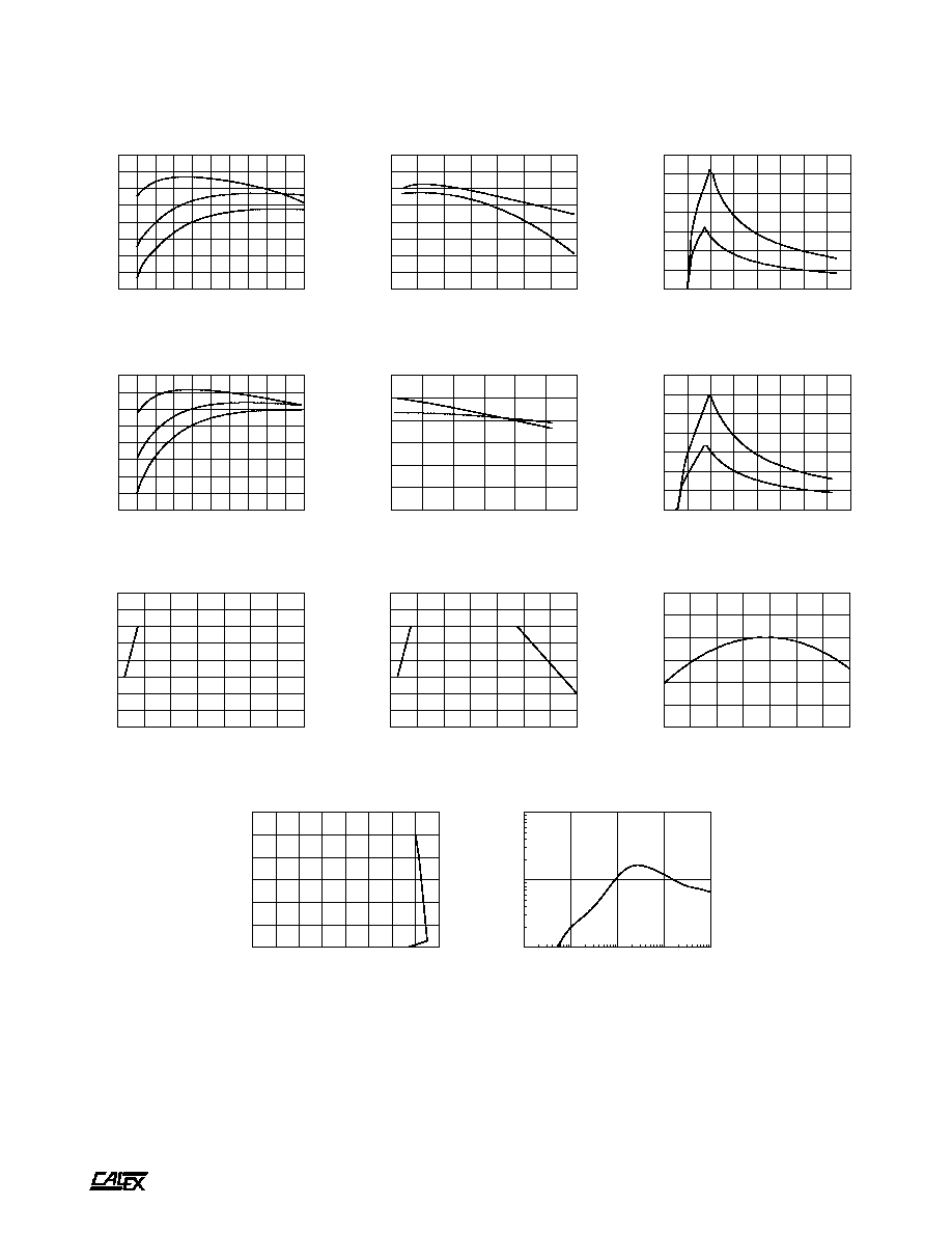
Typical Performance (Tc=25∞C, Vin=Nom VDC, Rated Load).
0
10
20
30
40
50
60
70
80
90
100
LOAD (%)
50
55
60
65
70
75
80
85
90
EFFICIENCY (%)
24 VOLT EFFICIENCY Vs. LOAD
LINE =
9VDC
LINE =
24VDC
LINE =
36VDC
8
12
16
20
24
28
32
36
LINE INPUT(VOLTS)
50
55
60
65
70
75
80
85
90
EFFICIENCY(%)
24 VOLT EFFICIENCY Vs. LINE INPUT VOLTAGE
45W LOAD
25W LOAD
0
5
10
15
20
25
30
35
40
LINE INPUT (VOLTS)
0
1
2
3
4
5
6
7
INPUT CURRENT (AMPS)
24 VOLT INPUT CURRENT Vs. LINE INPUT VOLTAGE
45W LOAD
25W LOAD
0
10
20
30
40
50
60
70
80
90
100
LOAD (%)
50
55
60
65
70
75
80
85
90
EFFICIENCY (%)
48 VOLT EFFICIENCY Vs. LOAD
LINE =
20VDC
LINE =
48VDC
LINE =
72VDC
20
30
40
50
60
70
80
LINE INPUT(VOLTS)
60
65
70
75
80
85
90
EFFICIENCY(%)
48 VOLT EFFICIENCY Vs. LINE INPUT VOLTAGE
45W LOAD
25W LOAD
0
10
20
30
40
50
60
70
80
LINE INPUT (VOLTS)
0.0
0.5
1.0
1.5
2.0
2.5
3.0
3.5
INPUT CURRENT (AMPS)
48 VOLT INPUT CURRENT Vs. LINE INPUT VOLTAGE
45W LOAD
25W LOAD
8
12
16
20
24
28
32
36
LINE INPUT (VDC)
70
75
80
85
90
95
100
105
110
OUTPUT POWER (%)
3.3 AND 5 VOLT 24S MODELS INPUT DERATING
8
12
16
20
24
28
32
36
LINE INPUT (VDC)
70
75
80
85
90
95
100
105
110
OUTPUT POWER (%)
12 AND 15 VOLT 24S MODELS INPUT DERATING
-40
-20
0
20
40
60
80
100
CASE TEMPERATURE (Deg C)
-0.4
-0.3
-0.2
-0.1
0.0
0.1
0.2
NORMALIZED OUTPUT (%)
OUTPUT VOLTAGE Vs. CASE TEMPERATURE
0
20
40
60
80
100
120
140
160
OUTPUT LOAD (%)
0
20
40
60
80
100
120
NORMALIZED OUTPUT (%)
OUTPUT VOLTAGE Vs. OUTPUT LOAD
CURRENT LIMIT MODE
"HICKUP" MODE
100
1000
10000
100000
1000000
FREQUENCY (Hz)
.01
.1
1
OUTPUT IMPEDANCE (OHMS)
TYPICAL OUTPUT IMPEDANCE Vs. FREQUENCY
NOTES ON USING THE CURVES
These curves were generated for 12 volt output models. To use for other models, adjust the efficiency values as shown:
3.3 volt models ................................. subtract approximately 4%
5.0 volt models ................................. subtract approximately 3%
15.0 volt models ............................... add approximately 1%

A
45 Watt XT Single Series DC/DC Converters
2401 Stanwell Drive ∑ Concord, California 94520 ∑ Ph: 925/687-4411 or 800/542-3355 ∑ Fax: 925/687-3333 ∑ www.calex.com ∑ Email: sales@calex.com
8
eco# 041007-1, eco# 050317-3, eco# 050929-4
Typical Performance (Tc=25∞C, Vin=Nom VDC, Rated Load).
8
12
16
20
24
28
32
36
LINE INPUT (VDC)
70
75
80
85
90
95
100
105
110
OUTPUT POWER (%)
3.3 AND 5 VOLT 24S MODELS INPUT DERATING
8
12
16
20
24
28
32
36
LINE INPUT (VDC)
70
75
80
85
90
95
100
105
110
OUTPUT POWER (%)
12 AND 15 VOLT 24S MODELS INPUT DERATING
-40
-20
0
20
40
60
80
100
CASE TEMPERATURE (Deg C)
-0.4
-0.3
-0.2
-0.1
0.0
0.1
0.2
NORMALIZED OUTPUT (%)
OUTPUT VOLTAGE Vs. CASE TEMPERATURE
0
20
40
60
80
100
120
140
160
OUTPUT LOAD (%)
0
20
40
60
80
100
120
NORMALIZED OUTPUT (%)
OUTPUT VOLTAGE Vs. OUTPUT LOAD
CURRENT LIMIT MODE
"HICKUP" MODE
100
1000
10000
100000
1000000
FREQUENCY (Hz)
.01
.1
1
OUTPUT IMPEDANCE (OHMS)
TYPICAL OUTPUT IMPEDANCE Vs. FREQUENCY
NOTES ON USING THE CURVES
These curves were generated for 12 volt output models. To use for other models, adjust the efficiency values as shown:
3.3 volt models ................................. subtract approximately 4%
5.0 volt models ................................. subtract approximately 3%
15.0 volt models ............................... add approximately 1%