 | –≠–ª–µ–∫—Ç—Ä–æ–Ω–Ω—ã–π –∫–æ–º–ø–æ–Ω–µ–Ω—Ç: CM1209 | –°–∫–∞—á–∞—Ç—å:  PDF PDF  ZIP ZIP |
© 2004 California Micro Devices Corp. All rights reserved.
01/09/04
430 N. McCarthy Blvd., Milpitas, CA 95035-5112
L Tel: 408.263.3214
L Fax: 408.263.7846 L www.calmicro.com
1
CM1209
4,6 & 8 Channel ESD Protection Arrays
with Zener Supply Clamp
Features
∑
Four, six or eight channels of ESD protection for
high data rate signals
∑
Zener diode protects supply rail and eliminates the
need for external by-pass capacitors
∑
+
15 kV contact,
+
15 kV air ESD protection per
channel (IEC 61000-4-2 standard)
∑
Low loading capacitance of 6pF typical
∑
Low supply current
∑
Available in miniature MSOP and SOIC packages
∑
Lead-free versions available
Applications
∑
ESD protection for a variety of electronic equip-
ment
∑
Set Top Boxes
∑
Digital TVs
∑
I/O & VGA Port protection
∑
Desktop and Notebook computers
∑
PDAs
∑
Cellular Phones
Product Description
The CM1209 family of diode arrays are designed to
provide either 4, 6 or 8 channels of ESD protection for
electronic components or sub-systems. Each channel
consists of a pair of diodes which steer the ESD cur-
rent pulse either to the positive (V
P
) or negative (V
N
)
supply. In addition, there is an integral Zener diode
between V
P
and V
N
to suppress any voltage distur-
bance due to these ESD current pulses. The CM1209
devices will protect against ESD pulses up to 15kV
contact discharge per the International Standard
IEC61000-4-2.
These devices are particularly well-suited for portable
electronics (e.g. cellular phones, PDAs, notebook com-
puters) because of its small package footprint, high
ESD protection level, and low loading capacitance.
They are also suitable for protecting video output lines
and I/O ports in computers, set top boxes, digital TVs
and peripheral equipment.
The CM1209 family of devices is optionally available
with lead-free finishing.
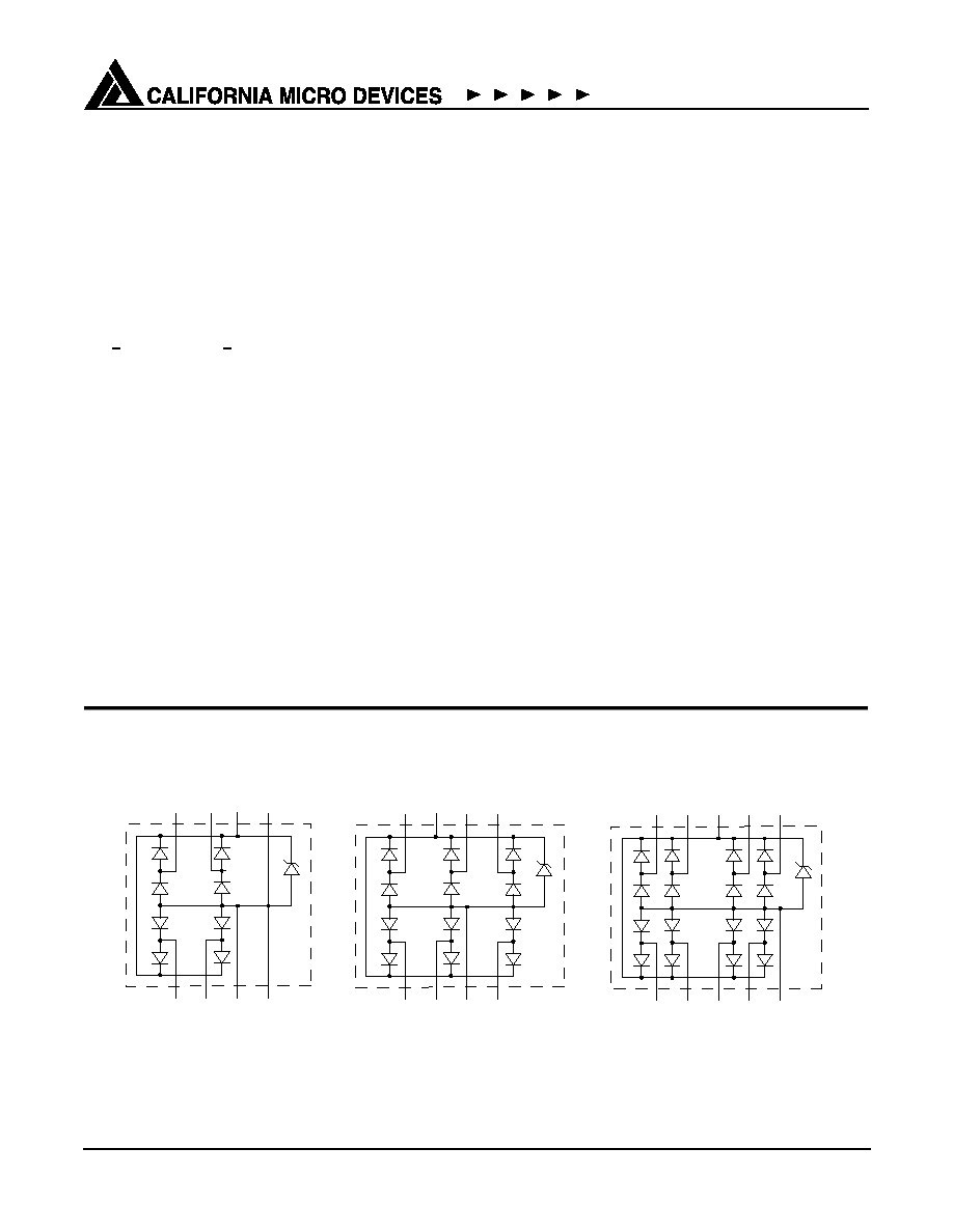
1
2
3
4
8
7
6
5
VP
VN
1
2
3
4
5
10 9
8
7
6
VP
VN
1
2
3
4
8
7
5
6
VP
VN
Electrical Schematics
CM1209-04
CM1209-06
CM1209-08
4-Channel
6-Channel
8-Channel
© 2004 California Micro Devices Corp. All rights reserved.
2
430 N. McCarthy Blvd., Milpitas, CA 95035-5112
L Tel: 408.263.3214
L Fax: 408.263.7846 L www.calmicro.com
01/09/04
CM1209
PIN DESCRIPTIONS
CM1209-04
CM1209-06
CM1209-08
NAME
PIN NO.
PIN NO
PIN NO
TYPE
DESCRIPTION
CH 1
1
1
1
I/O
ESD Channel 1
CH 2
2
2
2
I/O
ESD Channel 2
CH 3
7
4
3
I/O
ESD Channel 3
CH 4
8
5
4
I/O
ESD Channel 4
CH 5
6
6
I/O
ESD Channel 5
CH 6
8
7
I/O
ESD Channel 6
CH 7
9
I/O
ESD Channel 7
CH 8
10
I/O
ESD Channel 8
V
N
3,4,5
3
5
GND
Negative voltage supply rail or ground reference
rail.
V
P
6
7
8
Supply
Positive voltage supply rail.
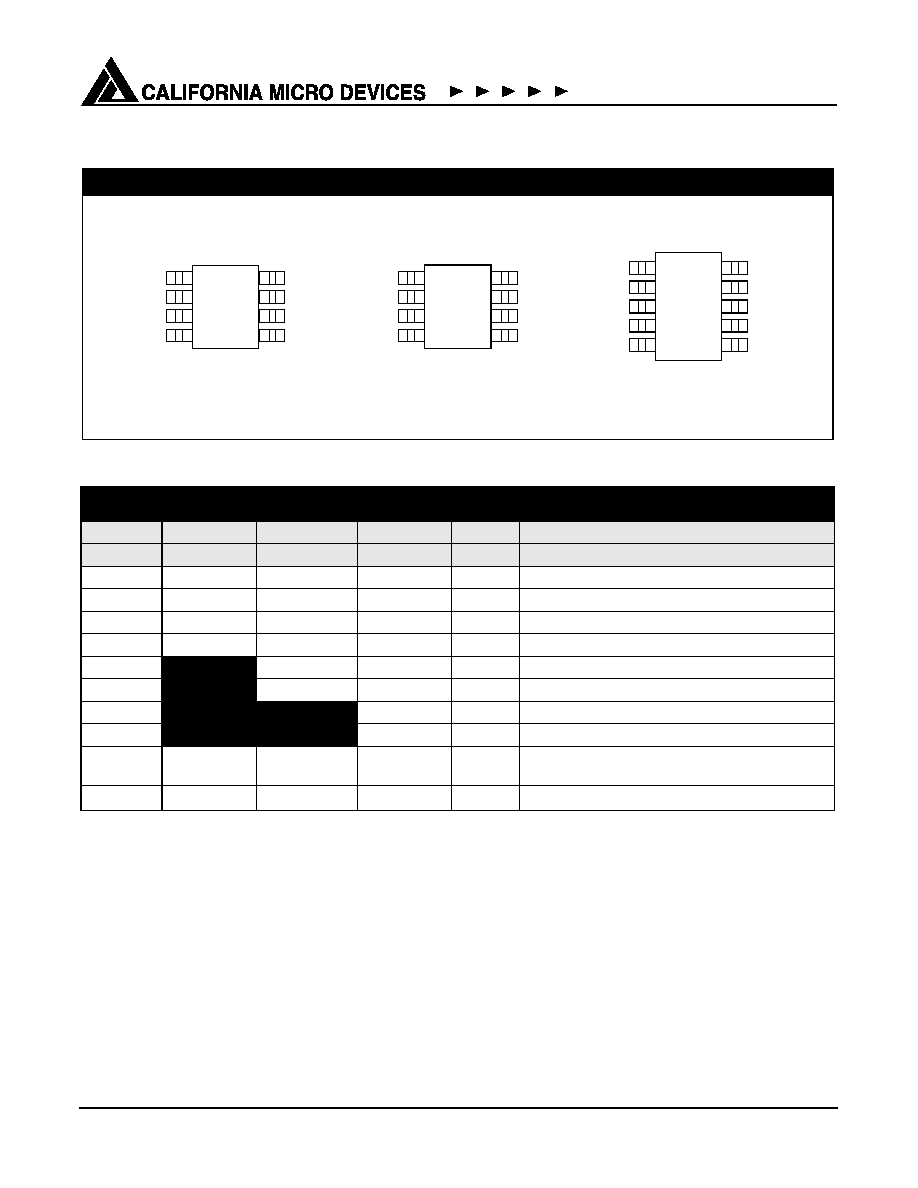
PACKAGE / PINOUT DIAGRAMS
Note: These drawings are not to scale.
8-pin SOIC/MSOP
1
2
3
4
8
7
6
5
CH 1
CH 2
V
N
CH 3
CH 6
V
P
CH 5
CH 4
TOP VIEW
CM1209-06SN/SM
8-pin MSOP
1
2
3
4
8
7
6
5
CH 1
CH 2
V
N
V
N
CH 4
CH 3
V
P
V
N
TOP VIEW
CM1209-04MS/MR
10-pin MSOP
1
2
3
4
10
9
8
7
CH 1
CH 2
V
N
CH 3
CH 8
CH 7
V
P
CH 6
TOP VIEW
CM1209-08MS/MR
5
6
CH 4
CH 5
CM1209-06MS/MR
© 2004 California Micro Devices Corp. All rights reserved.
01/09/04
430 N. McCarthy Blvd., Milpitas, CA 95035-5112
L Tel: 408.263.3214
L Fax: 408.263.7846
L www.calmicro.com
3
CM1209
Ordering Information
Note 1: Parts are shipped in Tape & Reel form unless otherwise specified.
Specifications
Note 1: Only one diode conducting at a time.
PART NUMBERING INFORMATION
# of Channels
Pins
Package
Standard Finish
Lead-free Finish
Ordering Part
Number
1
Part Marking
Ordering Part
Number
1
Part Marking
4
8
MSOP-8
CM1209-04MS
0904
CM1209-04MR 0914
6
8
SOIC-8
CM1209-06SN
CM1209-06S
CM1209-06SM
CM1209-06SM
6
8
MSOP-8
CM1209-06MS
0906
CM1209-06MR
0916
8
10
MSOP-10
CM1209-08MS
0908
CM1209-08MR
0918
ABSOLUTE MAXIMUM RATINGS
PARAMETER
RATING
UNITS
Supply Voltage (V
P
- V
N
)
6.0
V
Diode Forward DC Current (Note 1)
20
mA
Operating Temperature Range
-40 to +85
∞C
Storage Temperature Range
-65 to +150
∞C
DC Voltage at any channel input
(V
N
- 0.5) to (V
P
+ 0.5)
V
Package Power Rating
SOIC Package
MSOP Package
350
200
mW
mW
STANDARD OPERATING CONDITIONS
PARAMETER
RATING
UNITS
Operating Temperature Range
-40 to +85
∞C
Operating Supply Voltage (V
P
- V
N
)
0 to 5.5
V

© 2004 California Micro Devices Corp. All rights reserved.
4
430 N. McCarthy Blvd., Milpitas, CA 95035-5112
L Tel: 408.263.3214
L Fax: 408.263.7846 L www.calmicro.com
01/09/04
CM1209
Specifications (cont'd)
Note 1: All parameters specified at T
A
=-40 to +85∞C unless otherwise noted.
Note 2: These parameters guaranteed by design and characterization.
Note 3: From I/O pins to V
P
or V
N
only.
Note 4: Human Body Model per MIL-STD-883, Method 3015, C
Discharge
= 100pF, R
Discharge
= 1.5K
, V
P
= 5.0V, V
N
grounded.
Note 5: Standard IEC 61000-4-2 with C
Discharge
= 150pF, R
Discharge
= 330
, V
P
= 5.0V, V
N
grounded.
Note 6: These measurements performed with no external capacitor on V
P
..
ELECTRICAL OPERATING CHARACTERISTICS
(SEE NOTE 1)
SYMBOL
PARAMETER
CONDITIONS
MIN
TYP
MAX
UNITS
I
P
Supply Current
(V
P
-V
N
)=5.5V; T
A
=25∞C
10
µA
V
F
ESD Diode Forward Voltage
I
F
= 20mA; T
A
=25∞C
0.65
0.95
V
V
ZBD
Zener Clamp Reverse Breakdown
Voltage
At 1mA; T
A
=25∞C
7
V
I
LEAK
Channel Leakage Current
T
A
=25∞C
+0.1
+1.0
µA
C
IN
Channel Input Capacitance
At 1 MHz, V
P
=5V, via 10K;
V
N
=0V, V
IN
=2.5V;
Notes 2 and 6
6
8
pF
V
ESD
ESD Protection
Peak Discharge Voltage at any
channel input and V
P
rail
Contact discharge per
IEC 61000-4-2 standard
Air discharge per
IEC 61000-4-2 standard
Notes 2, 3, 5, and 6
Notes 2, 3, 5, and 6
+15
+15
kV
kV
V
CL
Channel Clamp Voltage
Positive Transients
Negative Transients
At 8kV ESD HBM;
T
A
=25∞C; Notes 2, 4 and 6
+12.5
- 5.1
V
V
Z
POS
Dynamic Resistance of Channel Input
for Positive Transients
I = 1A; T
A
=25∞C; See
Figure 2; Note 6 applies
0.70
Z
NEG
Dynamic Resistance of Channel Input
for Negative Transients
I = 1A; T
A
=25∞C; See
Figure 2; Note 6 applies
0.45
© 2004 California Micro Devices Corp. All rights reserved.
01/09/04
430 N. McCarthy Blvd., Milpitas, CA 95035-5112
L Tel: 408.263.3214
L Fax: 408.263.7846
L www.calmicro.com
5
CM1209
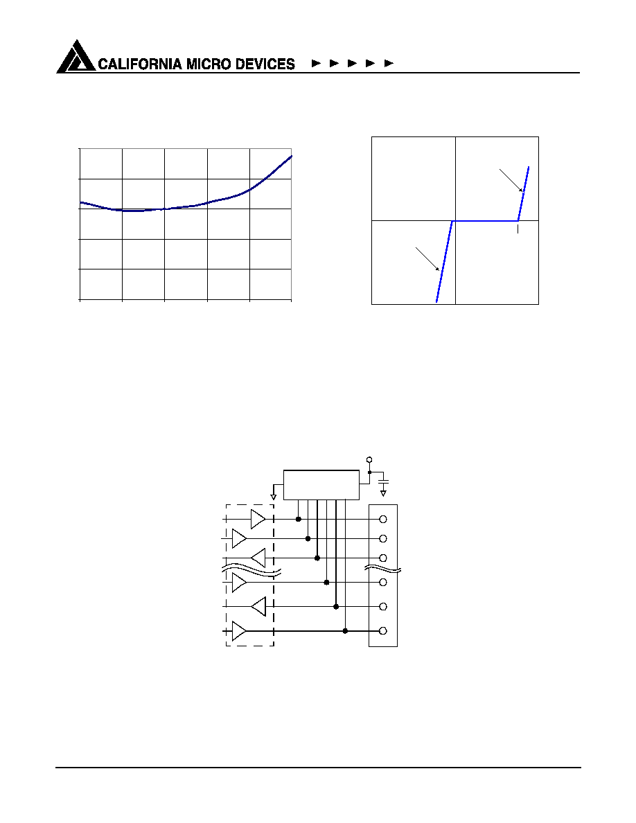
Performance Information
Figure 1. Typical Variation of Channel Input
Capacitance (C
IN
) vs. Channel Input Voltage (V
IN
)
(VP = 5V via 10K resistor, VN = 0V)
Figure 2. IV Curve for CM1209
Application Information
Figure 3. Application Example Using the CM1209-06 for I/O Port Protection
0
2
4
6
8
10
0
1
2
3
4
5
Vin
Ci
n
(
p
F
)
Slope = I/Z
POS
Slope = I/Z
NEG
Current [I]
Voltage [V]
V
ZBD
CM1209-06
I/O Port
Buffers
Connector
Expansion
Typical ESD Protection
1 2 4 5 6 8
7
3
0.22
µF*
* Optional capacitor should be placed as close as
possible to the V
P
pin on all CM1209 devices.
Refer to 'Design Considerations' text.