
©
2005 California Micro Devices Corp. All rights reserved.
06/30/05
430 N. McCarthy Blvd., Milpitas, CA 95035-5112
Tel: 408.263.3214
Fax: 408.263.7846
www.calmicro.com
1
CM1215
PRELIMINARY
1-, 2- and 4-Channel Low Capacitance ESD Arrays
Features
∑
1, 2, and 4 channels of ESD protection
∑
Provides
+
15 kV ESD protection on each channel
per the IEC 61000-4-2 ESD requirements
∑
Channel loading capacitance of 1.6 pF typical
∑
Channel I/O to GND capacitance difference of
0.04pF typical
∑
Mutual capacitance of 0.13pF typical
∑
Minimal capacitance change with temperature and
voltage
∑
Each I/O pin can withstand over 1000 ESD strikes
∑
SOT packages
∑
Lead-free versions available
Applications
∑
IEEE1394 Firewire
Æ
ports at 400Mbps / 800Mbps
∑
DVI ports, HDMI ports in notebooks, set top boxes,
digital TVs, LCD displays
∑
Serial ATA ports in desktop PCs and hard disk
drives
∑
PCI Express ports
∑
General purpose high-speed data line ESD protec-
tion
Product Description
The CM1215 family of diode arrays has been designed
to provide ESD protection for electronic components or
sub-systems requiring minimal capacitive loading.
These devices are ideal for protecting systems with
high data and clock rates or for circuits requiring low
capacitive loading. Each ESD channel consists of a
pair of diodes in series which steer the positive or neg-
ative ESD current pulse to either the positive (V
P
) or
negative (V
N
) supply rail. The CM1215 will protect
against ESD pulses up to
+
15kV per the IEC 61000-4-2
standard.
This device is particularly well-suited for protecting sys-
tems using high-speed ports such as USB2.0,
IEEE1394 (Firewire
Æ
, iLink
TM
), Serial ATA, DVI, HDMI
and corresponding ports in removable storage, digital
camcorders, DVD-RW drives and other applications
where extremely low loading capacitance with ESD
protection are required in a small package footprint.
The CM1215 family of devices is available with
optional lead-free finishing.
Simplified Electrical Schematic
CH1
V
P
V
N
CM1215-01ST/SO
CH1
V
P
V
N
CM1215-02ST/SO
CH2
CH1
V
P
V
N
CM1215-04ST/SO
CH4
CH2
CH3
CM1215-02SS/SR

©
2005 California Micro Devices Corp. All rights reserved.
2
430 N. McCarthy Blvd., Milpitas, CA 95035-5112
Tel: 408.263.3214
Fax: 408.263.7846
www.calmicro.com
06/30/05
CM1215
PRELIMINARY
Pin Configuration
Ordering Information
PACKAGE / PINOUT DIAGRAM
Note: These drawings are not to scale.
3-Pin SOT23-3
CH1
V
P
V
N
1
2
3
Top View
D151 /
4-Pin SOT143
1
4
2
3
D152 /
Top View
V
N
CH1
V
P
CH2
6-pin SOT23-6
1
2
6
5
3
4
D154 /
Top View
CH1
V
N
CH2
CH4
V
P
CH3
5-Lead SOT23-5
1
2
5
3
4
D152 /
Top View
NC
V
N
CH1
V
P
CH2
E152
E151
E152
E154
PACKAGE PIN DESCRIPTIONS
PIN
NAMER
SOT23-3
SOT143
SOT23-5
SOT23-6
TYPE
DESCRIPTION
PIN NO.
PIN NO.
PIN NO.
PIN NO.
CH1
1
2
3
1
I/O
ESD Channel
V
N
3
1
2
2
GND
Negative voltage supply
rail
CH2
-
3
4
3
I/O
ESD Channel
CH3
-
-
-
4
I/O
ESD Channel
V
P
2
4
5
5
PWR
Positive voltage supply rail
CH4
-
-
-
6
I/O
ESD Channel
N/C
-
-
1
-
-
No Connection
PART NUMBERING INFORMATION
Pins
Package
Standard Finish
Lead-free Finish
Ordering Part
Number
1
Part Marking
Ordering Part
Number
1
Part Marking
3
SOT23-3
CM1215-01ST
D151
CM1215-01SO
E151
4
SOT143
CM1215-02SS
D152
CM1215-02SR
E152
5
SOT23-5
CM1215-02ST
D152
CM1215-02SO
E152
6
SOT23-6
CM1215-04ST
D154
CM1215-04SO
E154

©
2005 California Micro Devices Corp. All rights reserved.
06/30/05
430 N. McCarthy Blvd., Milpitas, CA 95035-5112
Tel: 408.263.3214
Fax: 408.263.7846
www.calmicro.com
3
CM1215
PRELIMINARY
Specifications
ABSOLUTE MAXIMUM RATINGS
PARAMETER
RATING
UNITS
Operating Supply Voltage (V
P
-V
N
)
6
V
Diode Forward DC Current
(Note 1)
20
mA
DC Voltage at any Channel Input
(V
N
-0.5) to (V
P
+0.5)
V
Operating Temperature Range
Ambient
-40 to +85
∞C
Junction
-40 to +125
∞C
Storage Temperature Range
-40 to +150
∞C
STANDARD OPERATING CONDITIONS
PARAMETER
RATING
UNITS
Temperature Range (Ambient)
-40 to +85
∞C
Package Power Rating
SOT23-3 Package (CM1215-01ST/SO)
SOT143 Package (CM1215-02SS/SR)
SOT23-5 Package (CM1215-02ST/SO)
SOT23-6 Package (CM1215-04ST/SO)
225
225
225
225
mW
mW
mW
mW
©
2005 California Micro Devices Corp. All rights reserved.
4
430 N. McCarthy Blvd., Milpitas, CA 95035-5112
Tel: 408.263.3214
Fax: 408.263.7846
www.calmicro.com
06/30/05
CM1215
PRELIMINARY
Specifications (cont'd)
Note 1: All parameters specified at T
A
= -40∞C to +85∞C unless otherwise noted.
Note 2: These parameters guaranteed by design and characterization.
Note 3: Standard IEC 61000-4-2 with C
Discharge
= 150pF, R
Discharge
= 330
, V
P
= 3.3V, V
N
grounded.
Note 4: From I/O pins to V
P
or V
N
only. V
P
bypassed to V
N
with low ESR 0.2
F ceramic capacitor.
ELECTRICAL OPERATING CHARACTERISTICS
NOTE 1
SYMBOL
PARAMETER
CONDITIONS
MIN
TYP
MAX
UNIT
V
P
Operating Supply Voltage (V
P
-V
N
)
3.3
5.5
V
I
P
Operating Supply Current
(V
P
-V
N
) = 3.3V
8
A
V
F
Diode Forward Voltage
Top Diode
Bottom Diode
I
F
= 20mA; T
A
= 25∞C
0.6
0.6
0.8
0.8
0.95
0.95
V
V
I
LEAK
Channel Leakage Current
T
A
= 25∞C; V
P
= 5V,
V
N
= 0V
±0.1
±1.0
A
C
IN
Channel Input Capacitance
At 1 MHz, V
P
= 3.3V,
V
N
= 0V, V
IN
= 1.65V;
Note2
1.6
2.0
pF
C
IN
Channel I/O to GND Capacitance
Difference
Note 2
0.04
pF
C
MUTUAL
Mutual
Capacitance
(V
P
-V
N
) = 3.3V; Note 2
0.13
pF
V
ESD
ESD Protection
Peak Discharge Voltage at any
channel input, in system, contact
discharge per IEC 61000-4-2
standard
Notes 2, 3, and 4;
T
A
= 25∞C
±15
kV
V
CL
Channel Clamp Voltage
Positive Transients
Negative Transients
I
PP
= 1A, t
P
= 8/20
S;
T
A
=25∞C; Notes 2
V
P
+1.5
V
N
-1.5
V
V
R
DYN
Dynamic Resistance
Positive transients
Negative transients
I
PP
= 1A, t
P
= 8/20
S;
T
A
= 25∞C;
Notes 2
0.4
0.4
©
2005 California Micro Devices Corp. All rights reserved.
06/30/05
430 N. McCarthy Blvd., Milpitas, CA 95035-5112
Tel: 408.263.3214
Fax: 408.263.7846
www.calmicro.com
5
CM1215
PRELIMINARY
Performance Characteristics
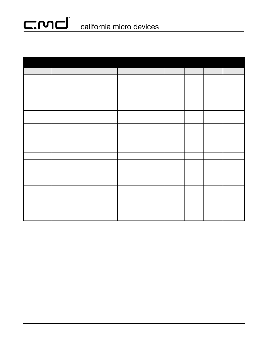
Input Channel Capacitance Performance Curve
Figure 1. Typical Variation of C
IN
vs. V
IN
(f = 1MHz, V
P
= 3.3V, V
N
= 0V, 0.1
F chip capacitor between V
P
and V
N
, T
A
= 25
∞
C)
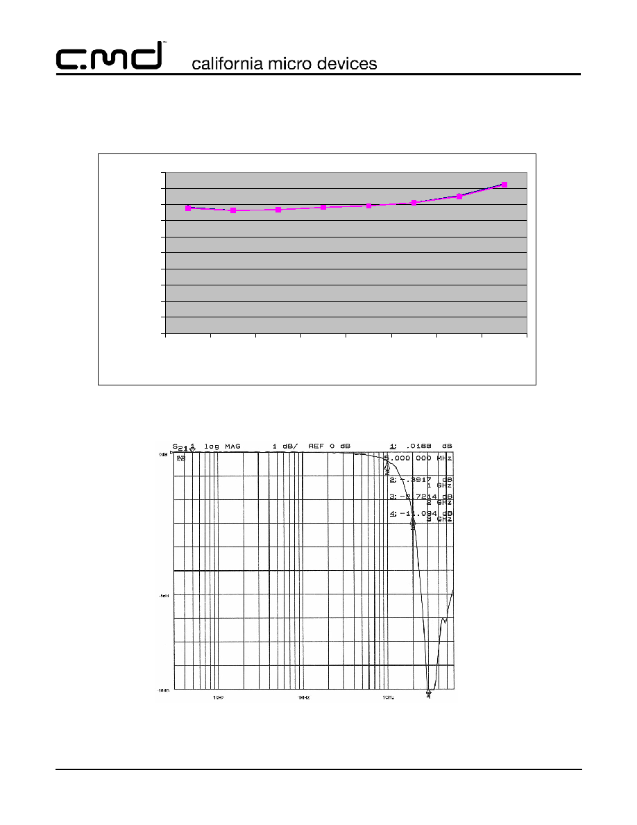
Figure 2. Typical Filter Performance (nominal conditions unless
specified otherwise, 50 Ohm Environment
0.000
0.200
0.400
0.600
0.800
1.000
1.200
1.400
1.600
1.800
2.000
0.00
0.50
1.00
1.50
1.65
2.00
2.50
3.00
Bias Voltage (V)
C
a
p
a
ci
t
a
n
ce (
p
F
)