©
2004 California Micro Devices Corp. All rights reserved.
12/22/04
430 N. McCarthy Blvd., Milpitas, CA 95035-5112
Tel: 408.263.3214
Fax: 408.263.7846
www.calmicro.com
1
CM1218
Low Capacitance Transient Voltage
Suppressors / ESD Protectors
Features
∑
Low I/O capacitance at 7pF typical
∑
In-system ESD protection to
±15kV contact
discharge, per the IEC 61000-4-2 international
standard
∑
Two, three, four or five channels of ESD protection
∑
Compact SMT package saves board space and
facilitates layout in space-critical applications
∑
Each I/O pin can withstand over 1000 ESD strikes
∑
Lead-free versions available
Applications
∑
High-speed consumer electronic ports
∑
ESD protection of PC ports, including USB ports,
serial ports, parallel ports, IEEE1394 ports,
docking ports, proprietary ports, etc.
∑
Protection of interface ports or IC pins which are
exposed to high ESD levels
Product Description
The CM1218 family of devices features transient volt-
age suppressor arrays that provide a very high level of
protection for sensitive electronic components which
may be subjected to electrostatic discharge (ESD).
All pins of the CM1218 are rated to withstand
±15kV
ESD pulses using the IEC 61000-4-2 contact dis-
charge method. Using the MIL-STD-883D (Method
3015) specification for Human Body Model (HBM)
ESD, all pins are protected from contact discharges of
greater than
±30kV.
The CM1218 is supplied in a number of compact, sur-
face mount packages depending on the channel con-
figuration desired. All versions of this device are
available with optional lead-free finishing.
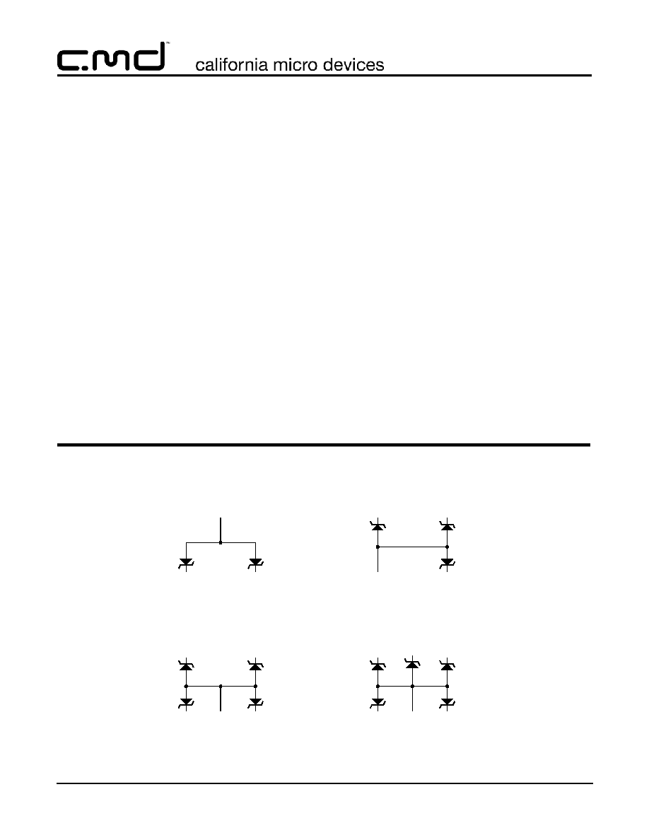
Electrical Schematics
V
N
1
2
4
3
CM1218-03
SOT-143
V
N
1
2
3
CM1218-02
SOT23-3
SC70-3
V
N
3
CM1218-04
SOT23-5 /
SC70-5
5
4
2
1
V
N
3
CM1218-05
SOT23-6 /
SC70-6
6
4
2
1
5
©
2004 California Micro Devices Corp. All rights reserved.
2
430 N. McCarthy Blvd., Milpitas, CA 95035-5112
Tel: 408.263.3214
Fax: 408.263.7846
www.calmicro.com
12/22/04
CM1218
Ordering Information
Note 1: Parts are shipped in Tape & Reel form unless otherwise specified.
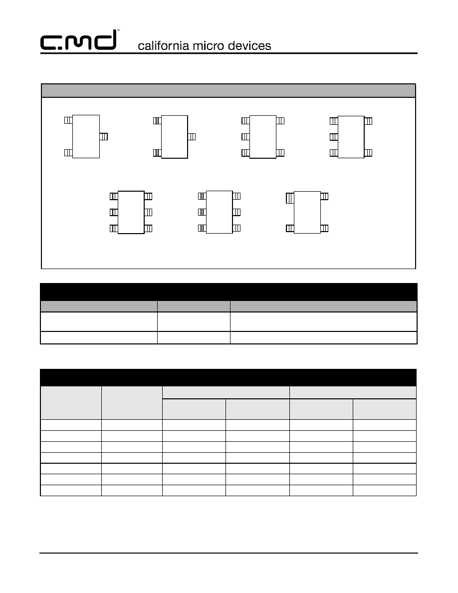
PIN DESCRIPTIONS
LEADS
NAME
DESCRIPTION
(Refer to package / pinout diagrams)
CHx
The cathode of the respective TVS diode, which should be
connected to the node requiring transient voltage protection.
(Refer to package / pinout diagrams)
V
N
The anode of the TVS diodes.
PACKAGE / PINOUT DIAGRAMS
Note: SOT23, SC70 and SOT143 and packages may differ in size. These drawings are not to scale.
3-lead SOT23
CH1
1
2
3
Top View
R2 /
3-lead SC70
1
2
3
Top View
R2 /
4-lead SOT143
1
4
2
3
R3 /
5-lead SOT23
1
2
5
3
4
R4 /
Top View
5-lead SC70
1
2
5
3
4
R4/
Top View
6-lead SC70
1
2
6
5
3
4
R5
/
6-lead SOT23
1
2
6
5
3
4
R5 /
Top View
Top View
Top View
R2R
R2R
R3R
R4R
R4R
R5R
R5
R
CH2
V
N
CH1
CH2
V
N
CH1
CH2
CH3
CH4
V
N
V
N
CH1
CH2
CH3
CH4
V
N
CH1
CH2
V
N
CH3
CH5
CH4
CH1
CH2
V
N
CH3
CH5
CH4
V
N
CH1
CH2
CH3
PART NUMBERING INFORMATION
Leads
Package
Standard Finish
Lead-free Finish
Ordering Part
Number
1
Part Marking
Ordering Part
Number
1
Part Marking
3
SOT23-3
CM1218-02ST
R2
CM1218-02SO
R2R
3
SC70-3
CM1218-02SC
R2
CM1218-02S7
R2R
4
SOT143
CM1218-03SS
R3
CM1218-03SR
R3R
5
SOT23-5
CM1218-04ST
R4
CM1218-04SO
R4R
5
SC70-5
CM1218-04SC
R4
CM1218-04S7
R4R
6
SOT23-6
CM1218-05ST
R5
CM1218-05SO
R5R
6
SC70-6
CM1218-05SC
R5
CM1218-05S7
R5R
©
2004 California Micro Devices Corp. All rights reserved.
12/22/04
430 N. McCarthy Blvd., Milpitas, CA 95035-5112
Tel: 408.263.3214
Fax: 408.263.7846
www.calmicro.com
3
CM1218
Specifications
Note 1: All parameters specified at T
A
= -40∞C to +85∞C unless otherwise noted.
Note 2: These parameters guaranteed by design and characterization.
Note 3: Human Body Model per MIL-STD-883, Method 3015, C
Discharge
= 100pF, R
Discharge
= 1.5K
, V
N
grounded.
Note 4: Standard IEC 61000-4-2 with C
Discharge
= 150pF, R
Discharge
= 330
, V
N
grounded.
Note 5: These measurements performed with no external capacitor on CH
X
.
ABSOLUTE MAXIMUM RATINGS
PARAMETER
RATING
UNITS
Storage Temperature Range
-65 to +150
∞C
Package Power Dissipation
SC70
SOT23-3, SOT23-5, SOT23-6, SOT143
0.2
0.225
W
W
STANDARD OPERATING CONDITIONS
PARAMETER
RATING
UNITS
Operating Temperature
-40 to +85
∞C
ELECTRICAL OPERATING CHARACTERISTICS
(NOTE 1)
SYMBOL PARAMETER
CONDITIONS
MIN
TYP
MAX
UNITS
C
IN
Channel Input Capacitance
T
A
= 25∞C, 2.5VDC, 1MHz; Note 2
7
pF
C
IN
Differential Channel I/O to GND
Capacitance
T
A
= 25∞C, 2.5VDC, 1MHz; Note 2
0.19
pF
V
RSO
Reverse Stand-off Voltage
I
R
=10
µA, T
A
= 25∞C
5.5
V
I
R
=1mA, T
A
= 25∞C
6.1
V
I
LEAK
Leakage Current
V
IN
=5.0VDC, T
A
= 25∞C
1
µ
A
V
SIG
Small Signal Clamp Voltage
Positive Clamp
Negative Clamp
I = 10mA, T
A
= 25∞C
I = -10mA, T
A
= 25∞C
6.8
-0.8
V
V
V
ESD
ESD Withstand Voltage
Contact Discharge per IEC 61000-
4-2 standard
Human Body Model, MIL-STD-883,
Method 3015
Notes 2, 4 & 5; T
A
= 25∞C
Notes 2, 3 & 5; T
A
= 25∞C
+15
+30
kV
kV
R
D
Diode Dynamic Resistance
Forward Conduction
Reverse Conduction
T
A
= 25∞C; Notes 2 & 3
1.1
2.7
©
2004 California Micro Devices Corp. All rights reserved.
4
430 N. McCarthy Blvd., Milpitas, CA 95035-5112
Tel: 408.263.3214
Fax: 408.263.7846
www.calmicro.com
12/22/04
CM1218
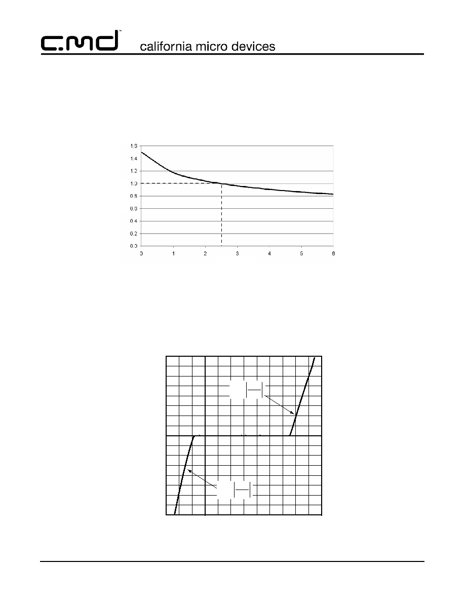
Performance Information
Diode Capacitance
Typical diode capacitance with respect to positive TVS cathode voltage (reverse voltage across the diode) is given
in
Figure 1
.
Figure 1. Diode Capacitance vs. Reverse Voltage
Typical High Current Diode Characteristics
Measurements are made in pulsed mode with a nominal pulse width of 0.7ms.
C
a
pacitanc
e
(
Normaliz
ed)
DC Voltage
Typical Input VI Characteristics
(Pulse-mode measurements, pulse width = 0.7ms nominal)
-1.6
-1.4
-1.2
-1.0
-0.8
-0.6
-0.4
-0.2
0.0
0.2
0.4
0.6
0.8
1.0
1.2
1.4
1.6
-3
-2
-1
0
1
2
3
4
5
6
7
8
9
Input Voltage (V)
Input
Current
(A)
R
D
=
1
slope
R
D
=
1
slope

©
2004 California Micro Devices Corp. All rights reserved.
12/22/04
430 N. McCarthy Blvd., Milpitas, CA 95035-5112
Tel: 408.263.3214
Fax: 408.263.7846
www.calmicro.com
5
CM1218
Mechanical Details
CM1218 devices are supplied in the following pack-
ages: SOT23-3, SOT143, SOT23-5, SOT23-6, SC70-3,
SC70-5, and SC70-6.
SOT23-3 Mechanical Specifications
Dimensions for CM1218-02ST/SO devices supplied in
3-pin SOT23 packages are presented below.
For complete information on the SOT23-3, see the Cal-
ifornia Micro Devices SOT23 Package Information doc-
ument.
Package Dimensions for SOT23-3.
PACKAGE DIMENSIONS
Package
SOT23-3 (JEDEC name is TO-236)
Pins
3
Dimensions
Millimeters
Inches
Min
Max
Min
Max
A
0.89
1.12
0.0350
0.0441
A1
0.01
0.10
0.0004
0.0039
b
0.30
0.50
0.0118
0.0197
c
0.08
0.20
0.0031
0.0079
D
2.80
3.04
0.1102
0.1197
E
2.10
2.64
0.0827
0.1039
E1
1.20
1.40
0.0472
0.0551
e
0.95 BSC
0.0374 BSC
e1
1.90 BSC
0.0748 BSC
L
0.40
0.60
0.0157
0.0236
L1
0.54 REF
0.0213 REF
# per tape
and reel
3000 pieces
Controlling dimension: millimeters
TOP VIEW
e
E1 E
2
e1
b
3
1
Mechanical Package Diagrams
A
SIDE VIEW
L1
END VIEW
D
A1
c
L