 | –≠–ª–µ–∫—Ç—Ä–æ–Ω–Ω—ã–π –∫–æ–º–ø–æ–Ω–µ–Ω—Ç: CM1484 | –°–∫–∞—á–∞—Ç—å:  PDF PDF  ZIP ZIP |
© 2006 California Micro Devices Corp. All rights reserved.
05/12/06
490 N. McCarthy Blvd., Milpitas, CA 95035-5112
Tel: 408.263.3214
Fax: 408.263.7846
www.cmd.com
1
CM1484
PRELIMINARY
Dual Channel EMI Filter with ESD Protection
Features
∑
Two channels of EMI filtering with integrated ESD
protection
∑
Pi-style EMI filters in a capacitor-resistor-capacitor
(C-R-C) network
∑
±15kV ESD protection on each channel
(IEC 61000-4-2 Level 4, contact discharge)
∑
±30kV ESD protection on each channel (HBM)
∑
Greater than 20dB attenuation (typical) at 1 GHz
∑
5-lead SC70 package
∑
Lead-free version available
Applications
∑
LCD and Camera data lines in mobile handsets
∑
I/O port protection for mobile handsets, notebook
computers, PDAs etc.
∑
EMI filtering for data ports in cell phones, PDAs or
notebook computers.
∑
Wireless handsets
∑
Handheld PCs/PDAs
∑
LCD and camera modules
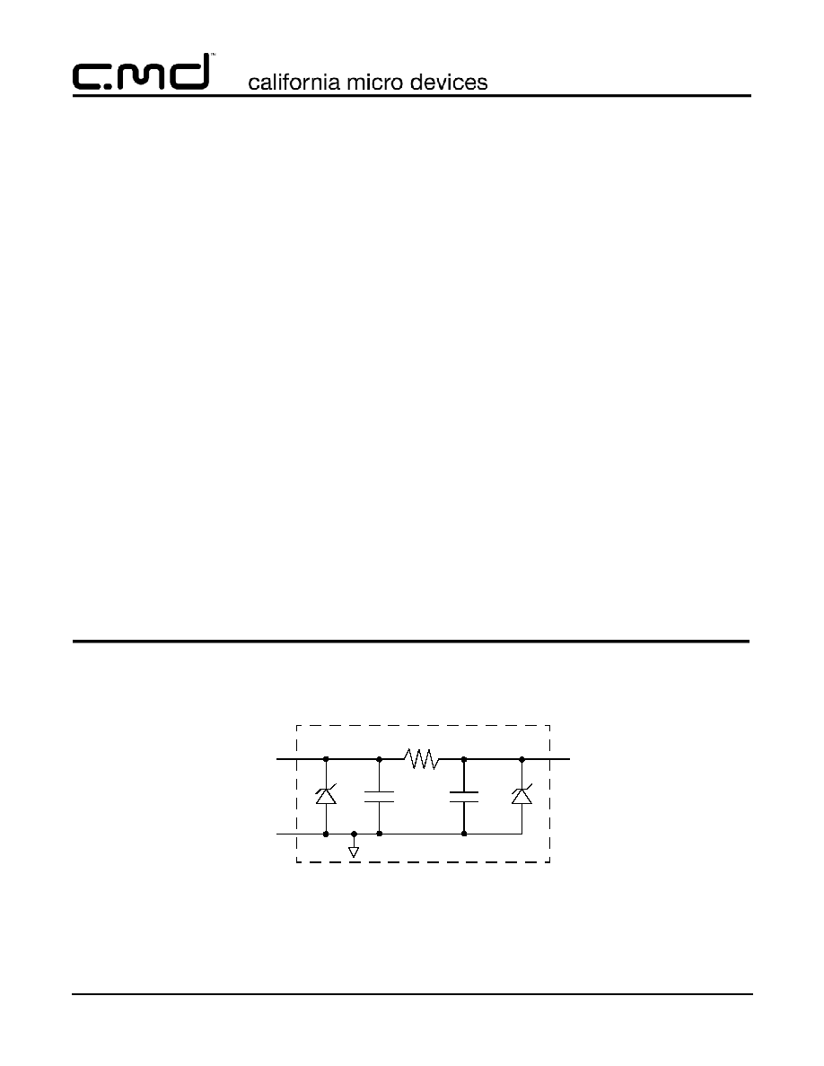
Product Description
The CM1484 is a 2 channel pi-style EMI filter array with
ESD protection, housed in a 5-lead SC-70 package.
The CM1484 has component values of 11pF-100
-
11pF per channel. The CM1484 has a cut-off fre-
quency of 220MHz and can be used in applications
with data rates up to 80Mbps. The parts include ESD
diodes on every pin, which provide a very high level of
protection for sensitive electronic components that may
be subjected to electrostatic discharge (ESD). The
ESD protection diodes safely dissipate ESD strikes of
±15kV, well beyond the maximum requirement of the
IEC61000-4-2 international standard. Using the MIL-
STD-883 (Method 3015) specification for Human Body
Model (HBM) ESD, the pins are protected for contact
discharges at greater than
±30kV.
These devices are particularly well-suited for portable
electronics (e.g. wireless handsets, PDAs, notebook
computers) because of their small package and easy-
to-use pin assignments. In particular, the CM1484 is
ideal for EMI filtering and protecting data and control
lines for the I/O data ports, LCD display and camera
interface in mobile handsets.
The CM1484 is housed in a small, 5-lead SC70 pack-
age and is available with lead-free finishing
.
100
11pF
11pF
FILTER+ESDn*
GND
FILTER+ESDn*
Electrical Schematic
1 of 2 EMI/RFI Filter Channels
* See Package/Pinout Diagram
for expanded pin information.
with Integrated ESD Protection
R
C
C
© 2006 California Micro Devices Corp. All rights reserved.
2
490 N. McCarthy Blvd., Milpitas, CA 95035-5112
Tel: 408.263.3214
Fax: 408.263.7846
www.cmd.com
05/12/06
CM1484
PRELIMINARY
Ordering Information
Note 1: Parts are shipped in Tape & Reel form unless otherwise specified.
Specifications
PIN DESCRIPTIONS
NAME
DESCRIPTION
1
FILTER1
Filter + ESD Channel 1
2
GND
Ground
3
FILTER2
Filter + ESD Channel 2
4
FILTER2
Filter + ESD Channel 2
5
FILTER1
Filter + ESD Channel 1
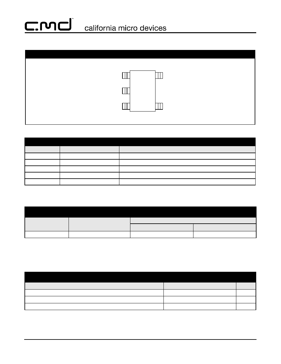
PACKAGE / PINOUT DIAGRAMS
Notes:
1) These drawings are not to scale.
5-lead SC70
1
2
5
3
4
Top View
N84R
CH1
CH2
CH2
CH1
GND
PART NUMBERING INFORMATION
Pins
Package
Lead-free Finish
Ordering Part Number
1
Part Marking
5
SC70
CM1484-02S7
N84R
ABSOLUTE MAXIMUM RATINGS
PARAMETER
RATING
UNITS
Storage Temperature Range
-65 to +150
∞C
DC Power per Resistor
100
mW
DC Package Power Rating
500
mW
© 2006 California Micro Devices Corp. All rights reserved.
05/12/06
490 N. McCarthy Blvd., Milpitas, CA 95035-5112
Tel: 408.263.3214
Fax: 408.263.7846
www.cmd.com
3
CM1484
PRELIMINARY
Note 1: T
A
=25
∞
C unless otherwise specified.
Note 2: ESD applied to input and output pins with respect to GND, one at a time.
Note 3: These parameters are guaranteed by design and characterization.
STANDARD OPERATING CONDITIONS
PARAMETER
RATING
UNITS
Operating Temperature Range
-40 to +85
∞C
ELECTRICAL OPERATING CHARACTERISTICS
(SEE NOTE1)
SYMBOL
PARAMETER
CONDITIONS
MIN
TYP
MAX
UNITS
R
Resistance
90
100
110
C
TOTAL
Total Channel Capacitance
At 0VDC Reverse
Bias, 1MHz, 30mVAC
17.6
22
26.4
pF
C
Capacitance C1
At 0VDC Reverse
Bias, 1MHz, 30mVAC
8.8
11
13.2
pF
I
LEAK
Diode Leakage Current (reverse bias)
V
DIODE
=+3.0V
1.0
A
V
Z
Zener Breakdown Voltage
Positive Clamp
I
LOAD
= 1mA
6.0
8.0
V
V
F
Zener Forward Voltage
I
F
= 50mA
1.5
V
V
ESD
In-system ESD Withstand Voltage
a) Human Body Model, MIL-STD-883, Method
3015
b) Contact Discharge per IEC 61000-4-2 Level 4
Notes 2 and 3
±30
±15
kV
kV
R
DYN
Dynamic Resistance
Positive
Negative
2.3
0.9
f
C
Cut-off Frequency
Z
SOURCE
=50
, Z
LOAD
=50
Channel R = 100
,
Channel C = 22pF at
0V reverse bias
220
MHz
© 2006 California Micro Devices Corp. All rights reserved.
4
490 N. McCarthy Blvd., Milpitas, CA 95035-5112
Tel: 408.263.3214
Fax: 408.263.7846
www.cmd.com
05/12/06
CM1484
PRELIMINARY
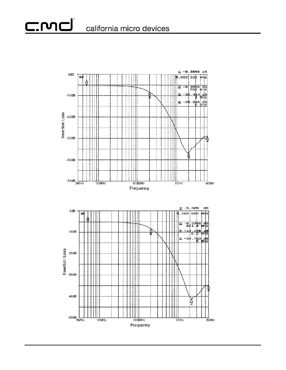
Performance Information
Typical Filter Performance (T
A
=25∞C, DC Bias=0V, 50 Ohm Environment)
Figure 1. Insertion Loss vs. Frequency (FILTER1 Input to GND)
Figure 2. Insertion Loss vs. Frequency (FILTER2 Input to GND)
© 2006 California Micro Devices Corp. All rights reserved.
05/12/06
490 N. McCarthy Blvd., Milpitas, CA 95035-5112
Tel: 408.263.3214
Fax: 408.263.7846
www.cmd.com
5
CM1484
PRELIMINARY
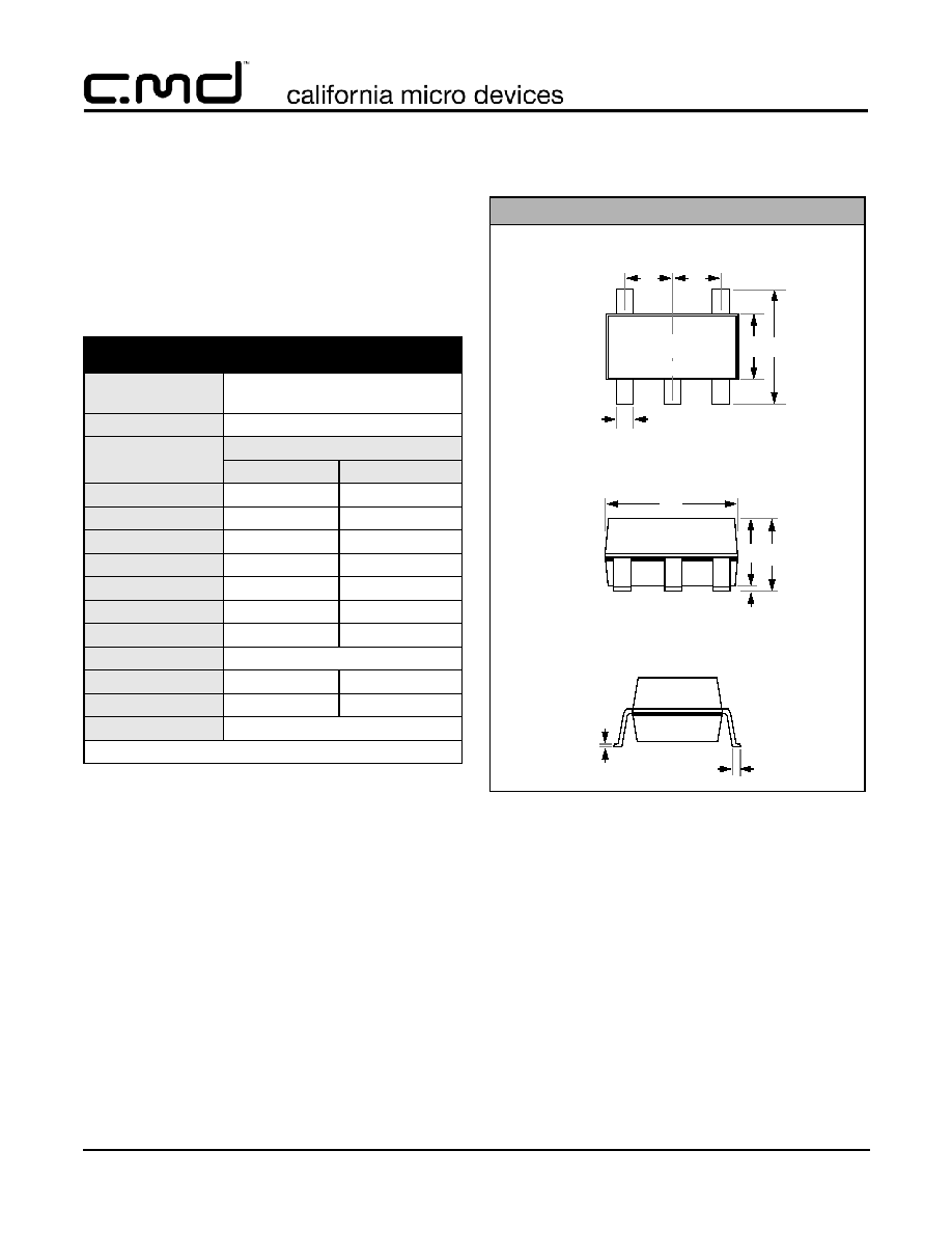
Mechanical Details
SC70-5 Mechanical Specifications:
The CM1484-02S7 is supplied in a 5-pin SC70 pack-
age. Dimensions are presented below.
For complete information on the SC70-5, see the Cali-
fornia Micro Devices SC70 Package Information docu-
ment.
Package Dimensions for SC70-5.
PACKAGE DIMENSIONS
Package
SC70-5
(JEDEC name is MO-203 Issue A)
Pins
5
Dimensions
Millimeters
Min
Max
A
0.80
1.10
A1
0.00
0.10
A2
0.70
1.00
B
0.15
0.30
c
0.08
0.25
D
1.85
2.25
E
1.15
1.35
e
0.65 BSC
HE
2.00
2.40
L
0.26
0.46
# / tape and reel
3000 pieces
Controlling dimension: millimeters
END VIEW
c
L
Mechanical Package Diagrams
TOP VIEW
e
e
E HE
B
A
SIDE VIEW
D
A2
A1
5
4
1
2
3