 | –≠–ª–µ–∫—Ç—Ä–æ–Ω–Ω—ã–π –∫–æ–º–ø–æ–Ω–µ–Ω—Ç: CM2010 | –°–∫–∞—á–∞—Ç—å:  PDF PDF  ZIP ZIP |
©
2004 California Micro Devices Corp. All rights reserved.
09/10/04
430 N. McCarthy Blvd., Milpitas, CA 95035-5112
Tel: 408.263.3214
Fax: 408.263.7846
www.calmicro.com
1
CM2010
PRELIMINARY
VGA Port Protection with Integrated Sync Buffers
Features
∑
3 channels of ESD protection for RGB output pins
meeting IEC-61000-4-2 Level 4 ESD requirements
(8kV contact discharge)
∑
Very low loading capacitance from ESD protection
diodes on VIDEO lines, 4pF typical
∑
3.3/5V 24mA buffer drivers for HSYNC and
VSYNC lines
∑
VESA Video Signal Standard (VSIS) - Version 1,
Rev. 2 Compatible Outputs
∑
Compact 10-lead MSOP package
∑
Lead-free version available
Applications
∑
VGA and DVI-I ports in:
- Desktop and Notebook PCs
- Graphics Cards
- Set Top Boxes
Product Description
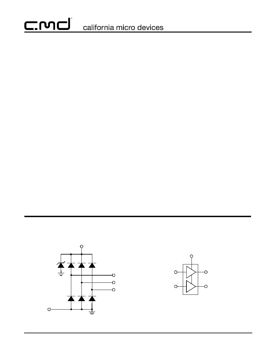
The CM2010 connects between a video graphics con-
troller, embedded in a PC or in a graphics adapter
card, and the VGA port connector. The CM2010 inte-
grates ESD protection for 3 VGA output signals imple-
mented with low-capacitance current steering diodes
such that an ESD pulse is diverted into either the posi-
tive supply rail or ground, where it may be safely dissi-
pated.
All ESD diodes are designed to safely handle the high
current spikes specified by IEC61000-4-2 Level 4 ESD
(8kV contact discharge).
Two 24mA non-inverting drivers provide buffering for
the HSYNC and VSYNC signals from the video control-
ler IC (SYNC1, SYNC2). These buffers accept low volt-
age input levels and convert them to CMOS output
levels that swing between Ground and V
CC_SYNC
,
which is typically 5V for Legacy VESA compatibility,
but can be operated at 3.3V. Additionally, the output
impedance of the drivers can be discretely adjusted via
external series termination resistors (R
T
) for maximum
flexibility. The output impedance of the drivers can be
adjusted over a wide range from 15
to over 100.
The CM2010 is supplied in a 10-lead MSOP package
and is available with optional lead-free finishing.
Simplified Electrical Schematic
VIDEO_1
VIDEO_2
VIDEO_3
V
CC_VIDEO
GND
V
CC_SYNC
3
4
5
6
2
9
SYNC_IN1
SYNC_IN2
SYNC_OUT1
SYNC_OUT2
7
8
10
1

©
2004 California Micro Devices Corp. All rights reserved.
2
430 N. McCarthy Blvd., Milpitas, CA 95035-5112
Tel: 408.263.3214
Fax: 408.263.7846
www.calmicro.com
09/10/04
CM2010
PRELIMINARY
Ordering Information
Note 1: Parts are shipped in Tape & Reel form unless otherwise specified.
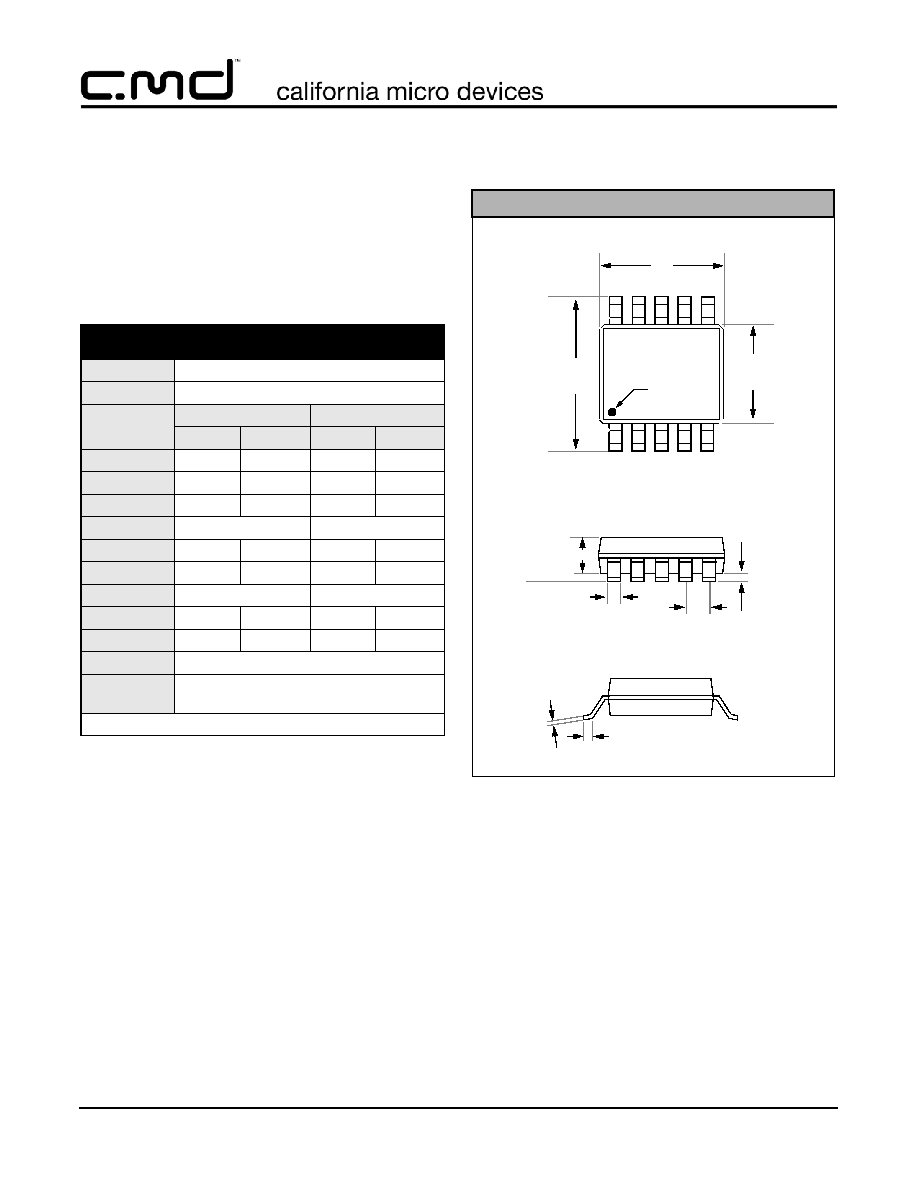
Pin Descriptions
PACKAGE / PINOUT DIAGRAM
Note: This drawing is not to scale.
10-PIN MSOP
1
2
3
4
10
9
8
7
V
CC_SYNC
V
CC_VIDEO
VIDEO_1
VIDEO_2
SYNC_OUT2
SYNC_IN2
SYNC_OUT1
SYNC_IN1
TOP VIEW
5
6
VIDEO_3
GND
PART NUMBERING INFORMATION
Pins
Package
Standard Finish
Lead-free Finish
Ordering Part
Number
1
Part Marking
Ordering Part
Number
1
Part Marking
10
MSOP
CM2010-02MS
2010 02MS
CM2010-02MR
2010 02MR
PIN DESCRIPTIONS
LEAD(s)
NAME
DESCRIPTION
1
V
CC_SYNC
This is an isolated supply input for the SYNC_1 and SYNC_2 level shifters and their associ-
ated ESD protection circuits.
2
V
CC_VIDEO
This is a supply pin specifically for the VIDEO_1, VIDEO_2 and VIDEO_3 ESD protection cir-
cuits.
3
VIDEO_1
Video signal ESD protection channel. This pin is typically tied one of the video lines between
the VGA controller device and the video connector.
4
VIDEO_2
Video signal ESD protection channel. This pin is typically tied one of the video lines between
the VGA controller device and the video connector.
5
VIDEO_3
Video signal ESD protection channel. This pin is typically tied one of the video lines between
the VGA controller device and the video connector.
6
GND
Ground reference supply pin.
7
SYNC_IN1
Sync signal buffer input. Connects to the VGA controller side of one of the sync lines.
8
SYNC_OUT1
Sync signal buffer output. Connects to the video connector side of one of the sync lines.
9
SYNC_IN2
Sync signal buffer input. Connects to the VGA controller side of one of the sync lines.
10
SYNC_OUT2
Sync signal buffer output. Connects to the video connector side of one of the sync lines.

©
2004 California Micro Devices Corp. All rights reserved.
09/10/04
430 N. McCarthy Blvd., Milpitas, CA 95035-5112
Tel: 408.263.3214
Fax: 408.263.7846
www.calmicro.com
3
CM2010
PRELIMINARY
Specifications
Note 1: All parameters specified over standard operating conditions unless otherwise noted.
Note 2: These parameters apply only to the SYNC drivers.
Note 3: Per the IEC-61000-4-2 International ESD Standard, Level 4 contact discharge method. BYP, V
CC
must be bypassed to
GND via a low impedance ground plane with a 0.22
µF, low inductance, chip ceramic capacitor at each supply pin. ESD
pulse is applied between the applicable pins and GND. ESD pulses can be positive or negative with respect to GND. Appli-
cable pins are: VIDEO_1, VIDEO_2 and VIDEO_3. All other pins are ESD protected to the industry standard
±2kV Human
Body Model (MIL-STD-883, Method 3015).
Note 4: This parameter is guaranteed by design and characterization.
Note 5: Rise and fall times measured between 0.5V and 2.4V.
ABSOLUTE MAXIMUM RATINGS
PARAMETER
RATING
UNITS
V
CC_VIDEO
and
V
CC_SYNC
Supply Voltage Inputs
6.0
V
ESD Clamp Diode Forward DC Current (applies only to SYNC drivers)
8
mA
DC Voltage at any channel Input
[GND - 0.5] to [V
CC
+ 0.5]
V
Operating Temperature Range
-40 to +85
∞C
Storage Temperature Range
-40 to +150
∞C
ELECTRICAL OPERATING CHARACTERISTICS
(SEE NOTE 1)
SYM-
BOL
PARAMETER
CONDITIONS
MIN TYP MAX UNITS
I
CC
V
CC
Supply Current
V
CC_SYNC
= 5V; SYNC inputs at GND or V
CC_SYNC
; SYNC
outputs unloaded
50
µA
V
CC_SYNC
= 5V; SYNC inputs at 3.0V;
SYNC outputs unloaded
2.0
mA
V
F
Diode Forward Voltage
I
F
= 10mA
1.0
V
V
IH
Logic High Input Voltage
V
CC_SYNC
= 5.0V; Note 2
1.5
V
V
IL
Logic Low Input Voltage
V
CC_SYNC
= 5.0V; Note 2
0.5
V
V
OH
Logic High Output Voltage
I
OH
= 8mA, V
CC_SYNC
= 3.0V; Note 2
2.0
V
I
OH
= 12mA, V
CC_SYNC
= 5.0V; Note 2
2.0
V
I
OH
= 24mA, V
CC_SYNC
= 5.0V; Note 2
2.0
V
V
OL
Logic Low Output Voltage
I
OL
= 8mA, V
CC_SYNC
= 3.3V; Note 2
0.8
V
I
OL
= 12mA, V
CC_SYNC
= 5.0V; Note 2
0.8
V
I
OL
= 24mA, V
CC_SYNC
= 5.0V; Note 2
0.8
V
R
OUT
SYNC Driver Output Resistance
V
CC_SYNC
= 5.0V; SYNC Inputs at GND or 3.0V
15
I
IN
Input Current
VIDEO Inputs
V
CC_VIDEO
= 5.0V; V
IN
= V
CC_VIDEO
or GND; T
A
=25∞C
±1
µA
SYNC_IN1, SYNC_IN2 Inputs
V
CC_SYNC
= 5.0V; V
IN
= V
CC_SYNC
or GND; T
A
=25∞C
±1
µA
C
IN_VID
VIDEO Input Capacitance
V
CC_VIDEO
= 5.0V; V
IN
= 2.5V;
= 1MHz; Note 4
4.0
pF
V
CC_VIDEO
= 2.5V; V
IN
= 1.25V;
= 1MHz; Note 4
4.5
pF
t
PLH
SYNC Driver L => H Propagation Delay
C
L
= 10pF; V
CC
= 5.0V; Input t
R
and t
F
5ns
12
ns
t
PHL
SYNC Driver H => L Propagation Delay
C
L
= 10pF; V
CC
= 5.0V; Input t
R
and t
F
5ns
12
ns
t
R,
t
F
SYNC Driver Output Rise & Fall Times
C
L
= 10pF; V
CC
= 5.0V; Input t
R
and t
F
5ns;
Notes 2, 4 & 5
3
ns
V
ESD
ESD Withstand Voltage
V
CC_VIDEO
= V
CC_SYNC
= 5V; Notes 3, 4
±8
kV
V
CL
Clamping Voltage during ESD Discharge
MIL-STD-883 (Method 3015), 8kV
Positive Transients
Negative Transients
Notes 3 and 4
+13
-13
V
V
©
2004 California Micro Devices Corp. All rights reserved.
4
430 N. McCarthy Blvd., Milpitas, CA 95035-5112
Tel: 408.263.3214
Fax: 408.263.7846
www.calmicro.com
09/10/04
CM2010
PRELIMINARY
Mechanical Details
MSOP Mechanical Specifications:
CM2010 devices are supplied in 10-pin MSOP pack-
ages. Dimensions are presented below.
For complete information on the MSOP-10 package,
see the California Micro Devices MSOP Package Infor-
mation document.
* This is an approximate number which may vary.
Package Dimensions for MSOP-10
PACKAGE DIMENSIONS
Package
MSOP
Pins
10
Dimensions
Millimeters
Inches
Min
Max
Min
Max
A
0.75
0.95
0.028
0.038
A1
0.05
0.15
0.002
0.006
B
0.18
0.40
0.006 0.016
C
0.18
0.007
D
2.90
3.10
0.114
0.122
E
2.90
3.10
0.114
0.122
e
0.50 BSC
0.0196 BSC
H
4.76
5.00
0.187
0.197
L
0.40
0.70
0.0137
0.029
# per tube
80 pieces*
# per tape
and reel
4000
Controlling dimension: inches
Mechanical Package Diagrams
E
D
H
1
2
3
4
10
9
8
7
L
END VIEW
C
e
B
A
A1
SEATING
PLANE
SIDE VIEW
TOP VIEW
6
5
Pin 1
Marking