 | –≠–ª–µ–∫—Ç—Ä–æ–Ω–Ω—ã–π –∫–æ–º–ø–æ–Ω–µ–Ω—Ç: CM2021 | –°–∫–∞—á–∞—Ç—å:  PDF PDF  ZIP ZIP |
©
2005 California Micro Devices Corp. All rights reserved.
03/22/05
430 N. McCarthy Blvd., Milpitas, CA 95035-5112
Tel: 408.263.3214
Fax: 408.263.7846
www.calmicro.com
1
CM2021
HDMI Receiver Port Protection and Interface Device
Features
∑
0.05pF matching capacitance between the TMDS
intra-pair
∑
Level shifting circuitry, including
±8kV
ESD protec-
tion on all TMDS lines
∑
Matched 0.5mm trace spacing (TSSOP)
∑
Simplified layout for HDMI connectors
∑
Backdrive protection
Applications
∑
PC
∑
Consumer Electronics
∑
Set Top Box
∑
Displays and Digital Television
Product Description
The CM2021 HDMI Receiver Port Protection and Inter-
face Device is specifically designed for next generation
HDMI Host interface protection.
An integrated package provides all ESD, level shift and
backdrive protection for an HDMI port in a single 38-
Pin TSSOP package.
The CM2021 part is specifically designed to comple-
ment the CM2020 protection part in HDMI receivers
(Displays, CE devices, etc.)
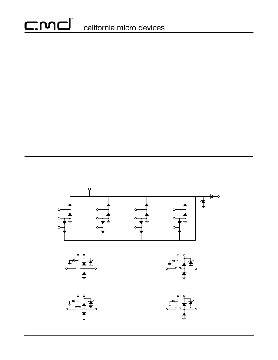
Electrical Schematic
TMDS_CK+
TMDS_GND
TMDS_CK-
TMDS_D2+
TMDS_GND
TMDS_D2-
TMDS_D1+
TMDS_GND
TMDS_D1-
TMDS_D0+
TMDS_GND
TMDS_D0-
TMDS_BYP
CE_REMOTE_OUT
CE_REMOTE_IN
DDC_CLK_OUT
DDC_CLK_IN
DDC_DAT_OUT
DDC_DAT_IN
HOTPLUG_DET_OUT
HOTPLUG_DET_IN
3.3V SUPPLY
TMDS_BYP
3.3V SUPPLY
TMDS_BYP
3.3V SUPPLY
TMDS_BYP
3.3V SUPPLY
TMDS_BYP
5V_SUPPLY

©
2005 California Micro Devices Corp. All rights reserved.
2
430 N. McCarthy Blvd., Milpitas, CA 95035-5112
Tel: 408.263.3214
Fax: 408.263.7846
www.calmicro.com
03/22/05
CM2021
PIN DESCRIPTIONS
PINS
NAME
DESCRIPTION
37
TMDS_BYP
This input pin is used to connect an optional external 0.1uF ceramic
bypass capacitor only to enhance the ESD protection level. Note: Do not
connect this pin to GND or any power rail.
4
TMDS_D2+
TMDS 0.9pF ESD protection.
33
TMDS_D2-
TMDS 0.9pF ESD protection.
7
TMDS_D1+
TMDS 0.9pF ESD protection.
30
TMDS_D1-
TMDS 0.9pF ESD protection.
10
TMDS_D0+
TMDS 0.9pF ESD protection.
27
TMDS_D0-
TMDS 0.9pF ESD protection.
13
TMDS_CK+
TMDS 0.9pF ESD protection.
24
TMDS_CK-
TMDS 0.9pF ESD protection.
16
CE_REMOTE_IN
3.3V_SUPPLY referenced logic level in.
23
CE_REMOTE_OUT
5V_SUPPLY referenced logic level out plus 3.5pF ESD.
17
DDC_CLK_IN
3.3V_SUPPLY referenced logic level in.
22
DDC_CLK_OUT
5V_SUPPLY referenced logic level out plus 3.5pF ESD.
18
DDC_DAT_IN
3.3V_SUPPLY referenced logic level in.
21
DDC_DAT_OUT
5V_SUPPLY referenced logic level out plus 3.5pF ESD.
19
HOTPLUG_DET_IN
3.3V_SUPPLY referenced logic level in.
20
HOTPLUG_DET_OUT
5V_SUPPLY referenced logic level out plus 3.5pF ESD.
2
3.3V_SUPPLY
Bias for CE / DDC / HOTPLUG level shifters.
1
5V_SUPPLY
Bias for CE / DDC / HOTPLUG level shifters plus current source for
5V_OUT.
6, 9, 12, 15, 26, 29,
32, 35, 38
NC
No connect.
3, 5, 8, 11, 14, 25,
28, 31, 34, 36
GND / TDMS_GND
GND reference.
1
2
3
4
5
6
7
8
9
38-PIN TSSOP PACKAGE
30
29
28
27
31
32
10
34
33
35
36
11
12
37
38
TMDS_GND
NC
TMDS_D1+
TMDS_GND
NC
TMDS_D0+
TMDS_GND
NC
5V_SUPPLY
3.3V_SUPPLY
GND
TMDS_D2+
TMDS_BYP
GND
NC
TMDS_GND
TMDS_D2-
NC
TMDS_GND
TMDS_D1-
NC
TMDS_GND
TMDS_D0-
NC
13
14
26
25
NC
TMDS_GND
TMDS_CK+
TMDS_GND
TOP VIEW
24
23
22
15
16
17
NC
CE_REMOTE_IN
DDC_CLK_IN
TMDS_CK-
CE_REMOTE_OUT
DDC_CLK_OUT
18
19
21
20
DDC_DAT_OUT
HOTPLUG_DET_OUT
DDC_DAT_IN
HOTPLUG_DET_IN
PACKAGE / PINOUT DIAGRAM
Note: This drawing is not to scale.

©
2005 California Micro Devices Corp. All rights reserved.
03/22/05
430 N. McCarthy Blvd., Milpitas, CA 95035-5112
Tel: 408.263.3214
Fax: 408.263.7846
www.calmicro.com
3
CM2021
Ordering Information
Note 1: Parts are shipped in Tape & Reel form unless otherwise specified.
Specifications
PART NUMBERING INFORMATION
Pins
Package
Standard Finish
Lead-free Finish
Ordering Part
Number
1
Part Marking
Ordering Part
Number
1
Part Marking
38
TSSOP-38
CM2021-00TS
CM2021-00TS
CM2021-00TR
CM2021-00TR
ABSOLUTE MAXIMUM RATINGS
PARAMETER
RATING
UNITS
V
CC5
, V
CC3
6.0
V
DC Voltage at any Channel Input
[GND - 0.5] to [VCC + 0.5]
V
Storage Temperature Range
-65 to +150
∞C
Operating Temperature Range
-40 to +85
∞C
STANDARD (RECOMMENDED) OPERATING CONDITIONS
SYMBOL
PARAMETER
MIN
TYP
MAX
UNITS
5V_SUPPLY
Operating Supply Voltage
5
5.5
V
3V_SUPPLY
Bias Supply Voltage
1
3.3
5.5
V

©
2005 California Micro Devices Corp. All rights reserved.
4
430 N. McCarthy Blvd., Milpitas, CA 95035-5112
Tel: 408.263.3214
Fax: 408.263.7846
www.calmicro.com
03/22/05
CM2021
Specifications (cont'd)
ELECTRICAL OPERATING CHARACTERISTICS
SYMBOL
PARAMETER
CONDITIONS
MIN
TYP
MAX
UNITS
I
CC5
Operating Supply Current
5V_SUPPLY = 5.0V
110
130
µA
I
CC3
Bias Supply Current
3.3V_SUPPLY = 3.3V
1
5
µA
I
OFF
OFF state leakage current,
level shifting NFET
3.3V_SUPPLY = 0V
0.1
5
µA
I
BACKDRIVE
Current conducted from output
pins to V_SUPPLY rails when
powered down
5V_SUPPLY
< V
CH_OUT
;
Signal pins: TMDS_[2:0]+/-,
TMDS_CK+/-, CE_REMOTE_OUT,
DDC_DAT_OUT, DDC_CLK_OUT,
HOTPLUG_DET_OUT Only
0.1
5
µA
V
ON
VOLTAGE drop across level
shifting NFET when ON
3.3V_SUPPLY = 2.5V, V
S
= GND,
I
DS
= 3mA
75
95
140
mV
V
F
Diode Forward Voltage
Top Diode
Bottom Diode
I
F
= 8mA, T
A
= 25∞C, Note 2
0.6
0.6
0.85
0.85
0.95
0.95
V
V
V
ESD
ESD Withstand Voltage (IEC)
Pins 4, 7,10,13, 20, 21, 22, 23, 24,
27, 30, 33;
Notes 2 and 3
±
8
kV
V
ESD
ESD Withstand Voltage
(HBM)
Pins 1, 2, 16, 17, 18, 19, 37;
Notes 2 and 4
±
2
kV
V
CL
Channel Clamp Voltage @
8kV HBM ESD
Positive Transients
Negative Transients
T
A
= 25∞C, Notes 2 and 4
9.0
-9.0
V
V
R
DYN
Dynamic Resistance
Positive Transients
Negative Transients
I = 1A, T
A
= 25∞C, Note 5
3.0
1.5
I
LEAK
TMDS Channel Leakage Cur-
rent
T
A
= 25∞C, Note 2
0.01
1
µA
C
IN,
TMDS
TMDS Channel Input
Capacitance
5V_SUPPLY = 5.0V,
Measured at 1MHz,
V
BIAS
=2.5V, Note 2
0.9
1.2
p
F
C
IN,
TMDS
C
IN
Matching Capacitance
5V_SUPPLY = 5.0V,
Measured at 1MHz,
V
BIAS
=2.5V, Note 2, 6
0.05
p
F
C
MUTUAL
Mutual Capacitance between
signal pin and NC pin
5V_SUPPLY= 0V,
Measured at 1MHz,
V
BIAS
=2.5V, Note 2
0.07
p
F
C
IN,
DDC
Level Shifting Input Capaci-
tance, Capacitance to GND
5V_SUPPLY = 0V,
Measured at 100KHz,
V
BIAS
=2.5V, Note 2
3.5
4
p
F

©
2005 California Micro Devices Corp. All rights reserved.
03/22/05
430 N. McCarthy Blvd., Milpitas, CA 95035-5112
Tel: 408.263.3214
Fax: 408.263.7846
www.calmicro.com
5
CM2021
Note 1: Operating Characteristics are over Standard Operating Conditions unless otherwise specified.
Note 2: This parameter is guaranteed by design and verified by device characterization.
Note 3: Standard IEC 61000-4-2, C
DISCHARGE
=150pF, R
DISCHARGE
=330
.
Note 4: Human Body Model per MIL-STD-883, Method 3015, C
DISCHARGE
=100pF, R
DISCHARGE
=1.5k
Note 5: These measurements performed with no external capacitor on TMDS_BYP.
Note 6: Intra-pair matching, each TMDS pair (i.e. D+, D-)
C
IN,
CEC
Level Shifting Input Capaci-
tance, Capacitance to GND
5V_SUPPLY = 0V,
Measured at 100KHz,
V
BIAS
=2.5V, Note 2
3.5
4
p
F
C
IN,
HP
Level Shifting Input Capaci-
tance, Capacitance to GND
5V_SUPPLY = 0V,
Measured at 100KHz,
V
BIAS
=2.5V, Note 2
3.5
4
p
F
ELECTRICAL OPERATING CHARACTERISTICS
©
2005 California Micro Devices Corp. All rights reserved.
6
430 N. McCarthy Blvd., Milpitas, CA 95035-5112
Tel: 408.263.3214
Fax: 408.263.7846
www.calmicro.com
03/22/05
CM2021
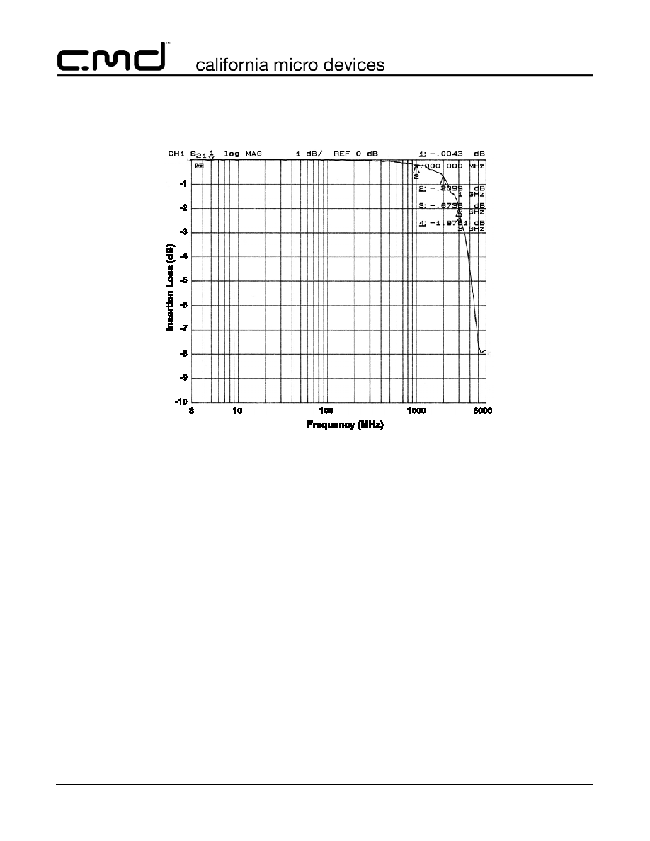
Performance Information
Typical Filter Performance (T
A
=25∞C, DC Bias=0V, 50 Ohm Environment)
Figure 1. Insertion Loss vs. Frequency (TMDS_D1- to GND)
©
2005 California Micro Devices Corp. All rights reserved.
03/22/05
430 N. McCarthy Blvd., Milpitas, CA 95035-5112
Tel: 408.263.3214
Fax: 408.263.7846
www.calmicro.com
7
CM2021
Application Information
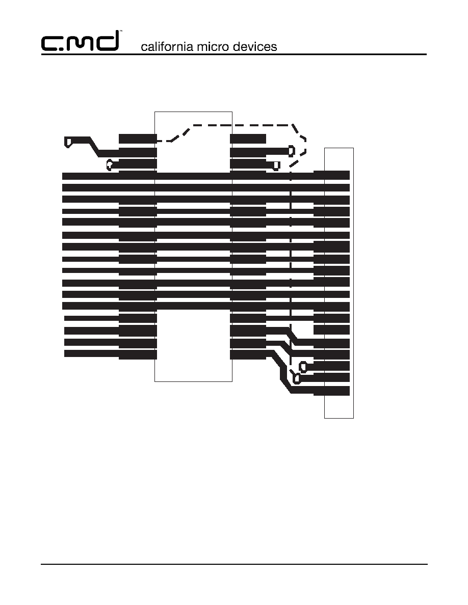
Figure 2. Typical Application for CM2021
HDMICONN
38 TSSOP
DDC_CLK
DDC_DAT
GND
+5V IN
HOTPLUG_DET
TMDS_CK-
CE REMOTE
N/C
TMDS_GND
TMDS_CK+
TMDS_D0-
TMDS_GND
TMDS_D0+
TMDS_D1-
TMDS_GND
TMDS_D1+
TMDS_D2-
TMDS_GND
TMDS_D2+
©
2005 California Micro Devices Corp. All rights reserved.
8
430 N. McCarthy Blvd., Milpitas, CA 95035-5112
Tel: 408.263.3214
Fax: 408.263.7846
www.calmicro.com
03/22/05
CM2021
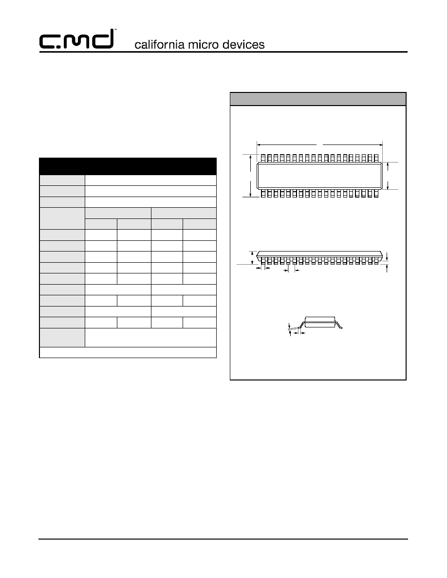
Mechanical Details
TSSOP-38 Mechanical Specifications
CM2021 devices are supplied in 38-pin TSSOP pack-
ages. Dimensions are presented below.
For complete information on the TSSOP-38, see the
California Micro Devices TSSOP Package Information
document.
Package Dimensions for TSSOP-38
PACKAGE DIMENSIONS
Package
TSSOP
JEDEC No.
MO-153 (Variation BD-1)
Pins
38
Dimensions
Millimeters
Inches
Min
Max
Min
Max
A
--
1.20
--
0.047
A1
0.05
0.15
0.002
0.006
b
0.17
0.27
0.007
0.011
c
0.09
0.20
0.004
0.008
D
9.60
9.80
0.378
0.386
E
6.40 BSC
0.252 BSC
E1
4.30
4.50
0.169
0.177
e
0.50 BSC
0.020 BSC
L
0.45
0.75
0.018
0.030
# per tape
and reel
2500 pieces
Controlling dimension: millimeters
15
24
16 17 18 19
23 22 21 20
Mechanical Package Diagrams
E1
D
E
TOP VIEW
L
END VIEW
c
e
b
A
A1
SEATING
PLANE
SIDE VIEW
5
6
7
8
9
10
1
2
3
4
34 33 32 31 30 29
38 37 36 35
Pin 1 Marking
11 12 13 14
28 27 26 25