©
2004 California Micro Devices Corp. All rights reserved.
08/24/04
430 N. McCarthy Blvd., Milpitas, CA 95035-5112
Tel: 408.263.3214
Fax: 408.263.7846
www.calmicro.com
1
CM2400-02/03/04
PRELIMINARY
Universal Serial Bus Transceiver with Level Translator
Features
∑
Complies with USB Specification Rev 1.1 & 2.0
∑
Supports full speed (12Mbit/sec.) and low speed
(1.5Mbits/sec.) modes
∑
Integrated 5V to 3.3V regulator
∑
Used as a USB device transceiver or
host transceiver
∑
V
BUS
disconnection indication through V
P
and V
M
outputs
∑
Two single-ended receivers with hysteresis
∑
USB Detection of V
BUS
via level translator
∑
Stable RCV output during SE0 condition
∑
Low power operation from V
CC
∑
Supports 1.65V to 3.6V I/O voltage levels
∑
Full industrial operating range -40 to 85 ∞C
∑
Available in small HBCC-16 and
TSSOP-16 packages
Applications
∑
Wireless handsets
∑
Digital still cameras
∑
PDAs (Personal Digital Assistants)
∑
IAs (Information Appliances)
Product Description
The CM2400-02/03/04 Universal Serial Bus (USB)
transceiver is fully compliant with the USB specification
Rev 1.1 and 2.0. It supports a speed of 12Mbits/s (Full
Speed Mode).
An internal level shifter allows interface to Application
Specific ICs (ASICs) and Programmable Logic Devices
(PLD's) running at core voltages of 1.65V to 3.6V.
The CM2400-02/03/04 features an internal 5V to 3.3V
regulator which is used to power the USB transceiver
via the USB supply V
BUS
.
The CM2400-04 features a Mode Input pin (MODE)
which allows the device to operate in either single or
differential input mode.
This device is ideal for portable electronic devices such
as mobile phones, digital still cameras, PDAs (Personal
Digital Assistants) and IAs (Information Appliances).
The CM2400-02/03/04 is packaged in a small form-fac-
tor 16-lead HBCC or TSSOP package to conserve
board space.
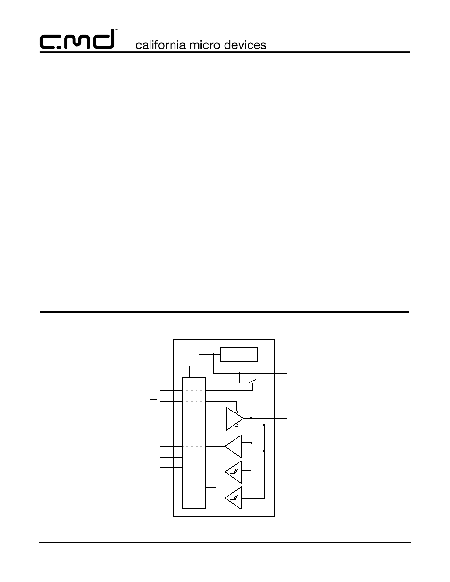
Simplified Block Schematic
Voltage
Regulator
V
CC
ENUM
OE
VMO/FSEO
VPO/VO
RCV
SPEED
V
P
V
M
GND
D-
D+
V
PU
V
BUS
SPND
L
EVEL TRANSLA
T
OR
V
REG
MODE*
* MODE pin available on
CM2400-04 only.
©
2004 California Micro Devices Corp. All rights reserved.
2
430 N. McCarthy Blvd., Milpitas, CA 95035-5112
Tel: 408.263.3214
Fax: 408.263.7846
www.calmicro.com
08/24/04
CM2400-02/03/04
PRELIMINARY
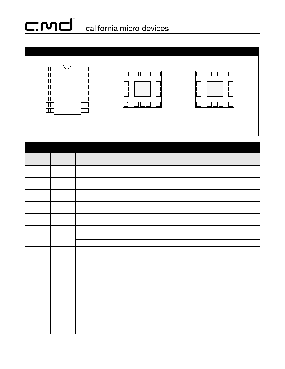
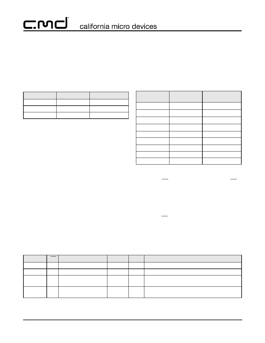
PIN DESCRIPTIONS
HBCC-16
PINS
TSSOP-16
PINS
NAME
DESCRIPTION
1
3
OE
Input for Output Enable (Active low). Enables transceiver driver to transmit data on
the USB bus. When OE pin = LOW, driver circuitry is enabled.
2
4
RCV
Differential receiver output of D+ and D- input data lines. The output state of RCV
is preserved and stable during an SE0 condition.
3
5
V
P
Single-ended D+ receiver output for detection of a single-ended zero or error con-
ditions
4
6
V
M
Single-ended D- receiver output for detection of a single-ended zero or error con-
ditions.
5
7
SPND
Suspend input. Allows the device to enter a low power state while the USB is inac-
tive.
6
8
MODE
Mode input (CM2400-04). Selects between differential (V
PO
, V
MO
) and single-
ended mode (V
O
, FSEO).
GND
Ground input (CM2400-02/03).
7
9
V
CC
Supply voltage for digital I/O pins. Voltages supported: 1.65 to 3.6V.
8
10
SPEED
Speed Input. If SPEED is logic '1', selects full speed. If SPEED is logic '0', selects
low speed. SPEED changes slope rise and fall time on D+ and D-.
9
11
D-
Negative USB data connection.
10
12
D+
Positive USB data connection. In full-speed connect mode, connect to V
PU
via a
1.5k
resistor. Tolerance of this resistor is defined in the USB specification REV
1.1 & 2.0
11
13
VPO/VO
Driver data input.
12
14
VMO/FSEO
Driver data input.
13
15
V
REG
Regulated supply voltage output during USB operation of V
BUS
. 1
µF decoupling
capacitor is required.
14
16
V
BUS
Supply voltage input. Can be directly connected to USB V
BUS
.
15
1
V
PU
Pull-up supply voltage. Pin function is controlled by input ENUM.
CM2400-02TS/-03TS
Top View
1
2
3
4
14
13
12
11
5
6
7
10
9
8
15
16
V
BUS
V
REG
VMO/FSEO
VPO/VO
D +
D -
SPEED
V
PU
ENUM
OE
RCV
V
P
V
M
SPND
V
CC
GND
CM2400-04HB
Bottom View
5
4
3
2
1
16
15 14
6
7
8
10
11
12
9
13
GND
HBCC-16
17
SPND
V
M
V
P
RCV
OE
ENU
M
V
BUS
V
PU
V
REG
VMO/FSEO
VPO/VO
D +
D -
SP
E
E
D
V
CC
GND
PACKAGE / PINOUT DIAGRAM
Note: These drawings are not to scale.
5
4
3
2
1
16
15 14
6
7
8
10
11
12
9
13
GND
HBCC-16
17
SPND
V
M
V
P
RCV
OE
ENU
M
V
BUS
V
PU
V
REG
VMO/FSEO
VPO/VO
D +
D -
SP
E
E
D
V
CC
MOD
E
CM2400-02HB/-03HB
Bottom View
©
2004 California Micro Devices Corp. All rights reserved.
08/24/04
430 N. McCarthy Blvd., Milpitas, CA 95035-5112
Tel: 408.263.3214
Fax: 408.263.7846
www.calmicro.com
3
CM2400-02/03/04
PRELIMINARY
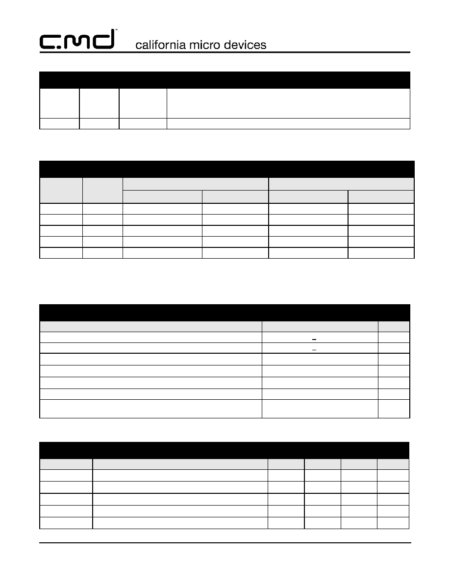
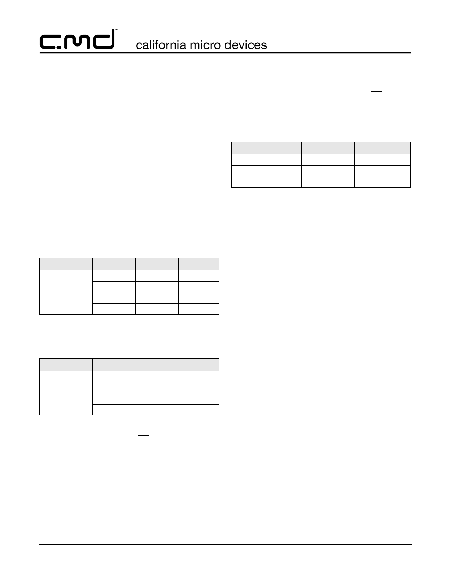
Ordering Information
Note 1: Parts are shipped in Tape & Reel form unless otherwise specified.
Note 2: Lead-free, 100% tin plated.
Specifications
Note 1: Equivalent to discharging a 100pF capacitor via a 1.5k
resistor (Human body model).
16
2
ENUM
Enumerate, allows software to control connection of the external pull-up via the
level translator. If ENUM = LOW then V
PU
is floating. If ENUM = HIGH then V
PU
is
internally connected to V
REG
.
17
-
GND
The ground terminal is connected to the exposed diepad (heatsink).
PIN DESCRIPTIONS (CONT'D)
PART NUMBERING INFORMATION
PADS/
LEADS
Package
Standard FInishing
Lead-free FInishing
2
Ordering Part Number
1
Part Marking
Ordering Part Number
1
Part Marking
16
HBCC-16
CM2400-02HB
CM240002HB
CM2400-02HA
CM240002HA
16
TSSOP-16
CM2400-02TS
CM240002TS
CM2400-02TR
CM240002TR
16
HBCC-16
CM2400-03HB
CM240003HB
CM2400-03HA
CM240003HA
16
TSSOP-16
CM2400-03TS
CM240003TS
CM2400-03TR
CM240003TR
16
HBCC-16
CM2400-04HB
CM240004HB
CM2400-04HA
CM240004HA
ABSOLUTE MAXIMUM RATINGS
PARAMETER
RATING
UNITS
ESD Protection (All Pins except D+/D- pins, HBM, See Note 1)
+1000
V
ESD Protection (D+/D- pins, HBM, See Note 1)
+4000
V
V
BUS
[GND - 0.5] to +5.5
V
V
CC
[GND - 0.5] to +6.0
V
V
I
(INPUT)
[GND - 0.5] to [V
CC
+ 0.5]
V
Storage Temperature Range
-65 to +150
∞C
Operating Temperature Range
Junction
-40 to +150
∞C
STANDARD (RECOMMENDED) OPERATING CONDITIONS
SYMBOL
PARAMETER
MIN
TYP
MAX
UNITS
V
BUS
USB V
BUS
Supply
4.0
5.0
5.5
V
V
CC
DC System Supply
1.65
3.3
3.6
V
V
I
DC Input Voltage
0
-
V
CC
V
V
I(AI/O)
Analog I/O Pins (D+, D-)
0
-
3.6
V
T
A
Ambient Operating Temperature Range
-40
-
+85
∞C
©
2004 California Micro Devices Corp. All rights reserved.
4
430 N. McCarthy Blvd., Milpitas, CA 95035-5112
Tel: 408.263.3214
Fax: 408.263.7846
www.calmicro.com
08/24/04
CM2400-02/03/04
PRELIMINARY
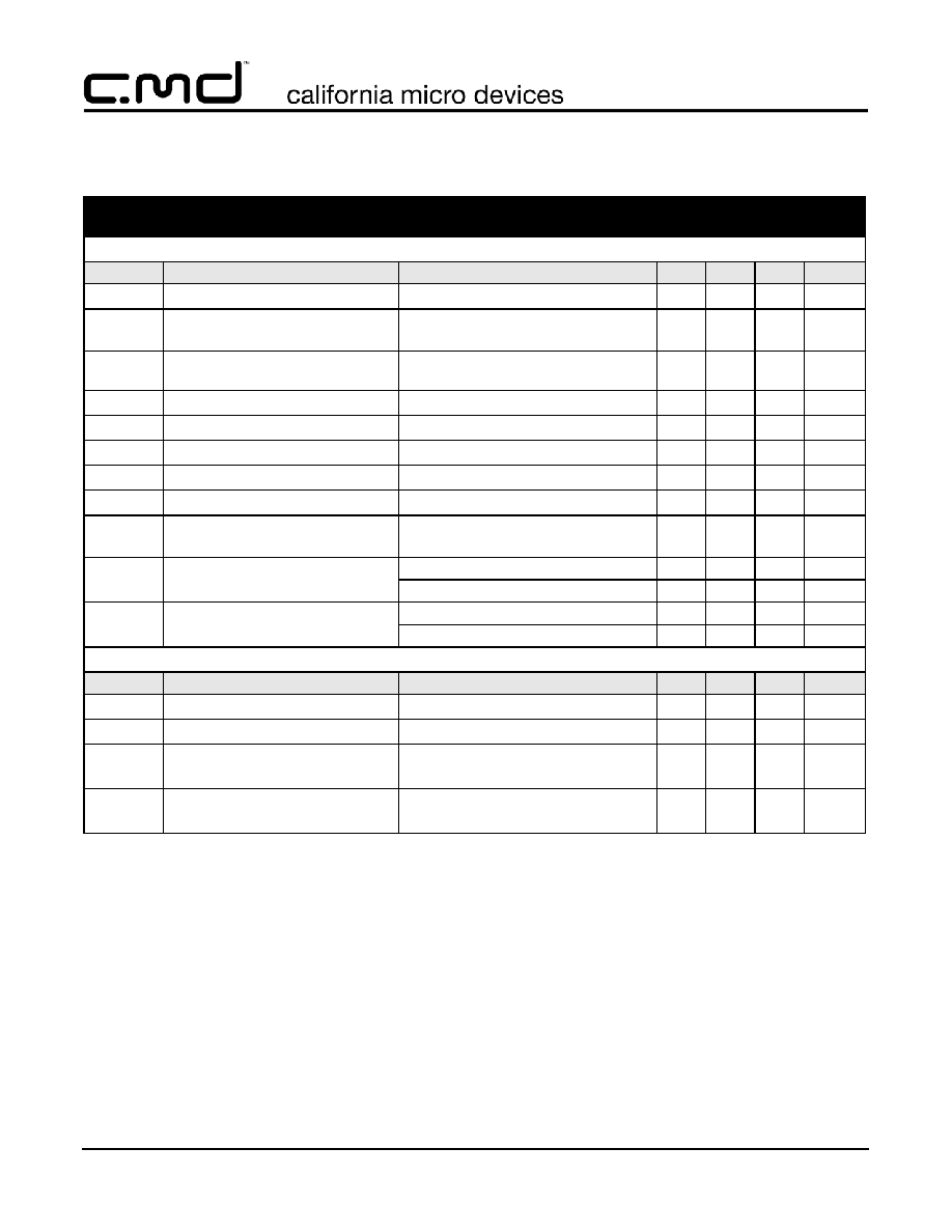
Specifications (cont'd)
Note 1: Operating Characteristics are over Standard Operating Conditions unless otherwise specified.
Note 2: Equivalent to discharging a 100pF capacitor via a 1.5k
resistor (Human body model).
Note 3: Excluding any load current and V
PU
/VSW source current to 1.5k
and 15k pull-up and pull-down resistors (200
µ
A).
Note 4: Current is drawn from VBUS of Host when device is a peripheral.
Note 5: Low current ideal for battery powered applications.
ELECTRICAL OPERATING CHARACTERISTICS
(SEE NOTE 1)
Supply Pins (V
BUS
= 4.0V to 5.5V; V
CC
= 1.65V to 3.6V)
SYMBOL
PARAMETER
CONDITIONS
MIN
TYP
MAX
UNITS
V
REG
Regulated supply output
Unloaded
3.0
3.3
3.6
V
I
BUS
Operating supply current
Full-speed TX and RX; C
L
=50pF on
D+/D- outputs; Note 2
8
mA
I
BUS(IDLE)
Supply current during full speed idle
and SE0
Full-speed idle; Notes 3 & 4
500
µ
A
I
BUS(DIS)
Disable mode supply current
V
CC
not present; Note 4
60
µ
A
I
BUS(SUSP)
Suspend mode supply current
SPND = HIGH; Notes 3 & 4
60
µ
A
I
CC
Operating I/O supply current
Full-speed TX and RX; Note 5
1.0
mA
I
CC(STAT)
Static I/O supply current
Full-speed idle, SE0 or suspend; Note 5
1.0
µ
A
I
CC(SHARE)
Supply current during sharing mode
V
BUS
not connected; Note 5
1.0
µ
A
I
DX(SHARE)
D+/D- load current during sharing
mode
V
BUS
not connected; ENUMERATE =
LOW; Note 5
1.0
µ
A
V
TH(VBUS)
V
BUS
supply detection threshold
Supply lost
0.8
V
Supply present
2.4
V
V
TH(VCC)
V
CC
supply detection threshold
Supply lost (USB_D low)
0.5
V
Supply present
1.4
V
Digital Pins (V
BUS
= 4.0V to 5.5V; V
CC
= 1.8V ± 0.15V)
SYMBOL
PARAMETER
CONDITIONS
MIN
TYP
MAX
UNITS
V
IL
Logic LOW input voltage
0.5
V
V
IH
Logic HIGH input voltage
1.2
V
V
OL
Logic LOW output voltage
I
OL
= 100
µA
I
OL
= 2mA
0.15
0.40
V
V
V
OH
Logic HIGH output voltage
I
OH
= 100
µA
I
OH
= 2mA
1.50
1.25
V
V
©
2004 California Micro Devices Corp. All rights reserved.
08/24/04
430 N. McCarthy Blvd., Milpitas, CA 95035-5112
Tel: 408.263.3214
Fax: 408.263.7846
www.calmicro.com
5
CM2400-02/03/04
PRELIMINARY
Specifications (cont'd)
Note 6: Rev 2.0 states Z
DRV
must be between 28
and 44, when the driver is not high speed capable.
ELECTRICAL OPERATING CHARACTERISTICS (CONT'D)
Digital Pins (V
BUS
= 4.0V to 5.5V; V
CC
= 2.5V ± 0.2V)
SYMBOL
PARAMETER
CONDITIONS
MIN
TYP
MAX
UNITS
V
IL
Logic LOW input voltage
0.7
V
V
IH
Logic HIGH input voltage
1.7
V
V
OL
Logic LOW output voltage
I
OL
= 100
µA
I
OL
= 2mA
0.15
0.40
V
V
V
OH
Logic HIGH output voltage
I
OH
= 100
µA
I
OH
= 2mA
2.15
1.90
V
V
Digital Pins (V
BUS
= 4.0V to 5.5V; V
CC
= 1.65V to 3.6V)
SYMBOL
PARAMETER
CONDITIONS
MIN
TYP
MAX
UNITS
V
IL
Logic LOW input voltage
0.3
V
CC
V
V
IH
Logic HIGH input voltage
0.6
V
CC
V
V
OL
Logic LOW output voltage
I
OL
= 100
µA
I
OL
= 2mA
0.15
0.40
V
V
V
OH
Logic HIGH output voltage
I
OH
= 100
µA
I
OH
= 2mA
V
CC
- 0.15
V
CC
- 0.40
V
V
Analog I/O Pins (V
BUS
= 4.0V to 5.5V; V
CC
= 1.65V to 3.6V)
SYMBOL
PARAMETER
CONDITIONS
MIN
TYP
MAX
UNITS
V
DI
Differential receiver input
sensitivity
|
V
I
(D+) - V
I
(D-)
|
0.2
V
V
CM
Differential receiver
common mode voltage
0.8
2.5
V
V
IL
Single-ended receiver
logic LOW input voltage
0.8
V
V
IH
Single-ended receiver
logic HIGH input voltage
2.0
V
V
HYS
Single-ended receiver
Hysteresis voltage
0.4
0.7
V
V
OL
Logic LOW output voltage
R
L
= 1.5K
tied to +3.6V
0.3
V
V
OH
Logic HIGH output voltage
R
L
= 15K
tied to GND
2.8
3.6
V
I
LZ
OFF-state leakage current
+1
µ
A
C
IN
Transceiver Capacitance
Pin to GND
20
pF
R
SW
Internal switch resistance at
V
PU
50
Z
DRV
Driver output impedance
(includes 33 ohm 1% resis-
tor)
Measured with steady-state drive;
See Note 6
28
39
44

©
2004 California Micro Devices Corp. All rights reserved.
6
430 N. McCarthy Blvd., Milpitas, CA 95035-5112
Tel: 408.263.3214
Fax: 408.263.7846
www.calmicro.com
08/24/04
CM2400-02/03/04
PRELIMINARY
Specifications (cont'd)
ELECTRICAL OPERATING CHARACTERISTICS (CONT'D)
Driver Characteristics & Timings (Full-speed mode only, SPEED=HIGH)
SYMBOL
PARAMETER
CONDITIONS
MIN
TYP
MAX
UNITS
t
FR
Rise time
C
L
= 50 to 125pF, measured 10% to 90%
(V
OH
-V
OL
); See Figure 6
4
20
ns
t
FF
Fall time
C
L
= 50 to 125pF, measured 10% to 90%
(V
OH
-V
OL
); See Figure 6
4
20
ns
FRFM
Differential rise / fall time
matching (t
FR
/ t
FF
)
Excluding the first transition from idle state
100
%
V
CRS
Output signal crossover
voltage
Excluding the first transition from idle state;
See Figure 9
1.65
V
t
PLH(DRV)
Driver propagation delay
(V
O
/ V
PO
D+ / D- ;
FSEO / V
MO
D+ / D-
LOW-to-HIGH transition; See Figure 9
18
ns
t
PHL(DRV)
HIGH-to-LOW transition; See Figure 9
18
ns
t
PHZ
Driver disable delay
(OE
D+ / D-)
HIGH-to-OFF; See Figure 7
15
ns
t
PLZ
LOW-to-OFF; See Figure 7
15
ns
t
PZH
Driver enable delay
(OE
D+ / D-)
OFF-to-HIGH; See Figure 7
15
ns
t
PZL
OFF-to-LOW; See Figure 7
15
ns
Driver Characteristics & Timings (Low-speed mode only, SPEED=LOW)
SYMBOL
PARAMETER
CONDITIONS
MIN
TYP
MAX
UNITS
t
LR
Rise time
C
L
= 200 to 600pF, measured 10% to 90%
(V
OH
-V
OL
); See Figure 6
75
300
ns
t
LF
Fall time
C
L
= 200 to 600pF, measured 10% to 90%
(V
OH
-V
OL
); See Figure 6
75
300
ns
FRFM
Differential rise / fall time
matching (t
FR
/ t
FF
)
Excluding the first transition from idle state
80
125
%
V
CRS
Output signal crossover
voltage
Excluding the first transition from idle state;
See Figure 9
1.3
2.0
V
Receiver Timings (Full-speed and low-speed modes)
SYMBOL
PARAMETER
CONDITIONS
MIN
TYP
MAX
UNITS
Differential Receiver
t
PLH(RCV)
Driver propagation delay
(D+ / D-
RCV)
LOW-to-HIGH transition; See Figure 8
15
ns
t
PHL(RCV)
HIGH-to-LOW transition; See Figure 8
15
ns
Single-ended Receiver
t
PLH(SE)
Driver propagation delay
(D+ / D-
V
P
/ V
M
)
LOW-to-HIGH transition; See Figure 8
18
ns
t
PHL(SE)
HIGH-to-LOW transition; See Figure 8
18
ns
©
2004 California Micro Devices Corp. All rights reserved.
08/24/04
430 N. McCarthy Blvd., Milpitas, CA 95035-5112
Tel: 408.263.3214
Fax: 408.263.7846
www.calmicro.com
7
CM2400-02/03/04
PRELIMINARY
Specifications (cont'd)
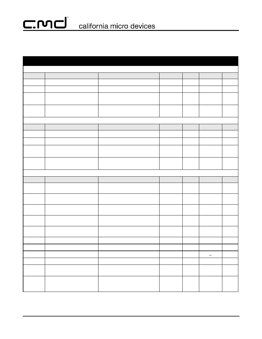
Test Loads
Load for V
P
/ V
M
and
Load for D+ and D- delay measurements
Load for ENABLE and DISABLE
V = V
REG
(3.3) for t
PZL
and t
PLZ
V = 0 v for t
PZH
and t
PHZ
DUT
Test Point
15pF
DUT
Test Point
50pF
33
15
k
DUT
Test Point
50pF
33
200
V
RCV delay measurements
(MAX and MIN Timing)
delay measurements.
©
2004 California Micro Devices Corp. All rights reserved.
8
430 N. McCarthy Blvd., Milpitas, CA 95035-5112
Tel: 408.263.3214
Fax: 408.263.7846
www.calmicro.com
08/24/04
CM2400-02/03/04
PRELIMINARY
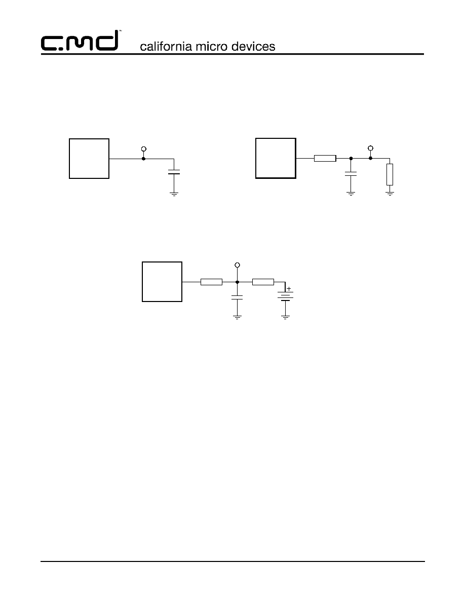
Performance Information
CM2400-02/03/04 Typical DC Characteristics (nominal conditions unless specified otherwise)
Figure 1. V
CC
Current in Idle Mode (SPND=LOW)
Figure 2. V
CC
Current in Suspend Mode
(SPND=HIGH)
Figure 3. V
BUS
Current in Idle Mode (SPND=LOW)
Figure 4. V
BUS
Current in Suspend Mode
(SPND=HIGH)
-1.00
-0.50
0.00
0.50
1.00
1.6 1.8 2.0 2.2 2.4 2.6 2.8 3.0 3.2 3.4
VCC VOLTAGE[V]
V
CC
CURRE
NT
[
µ
A]
-1.00
-0.50
0.00
0.50
1.00
1.6 1.8 2.0 2.2 2.4 2.6 2.8 3.0 3.2 3.4
VCC VOLTAGE[V]
V
CC
CURRE
N
T
[
µ
A]
100
150
200
250
300
4.1
4.3
4.5
4.7
4.9
5.1
5.3
5.5
VBUS VOLTAGE[V]
V BUS
CURRE
NT
[
µ
A]
40.0
45.0
50.0
55.0
60.0
4.1
4.3
4.5
4.7
4.9
5.1
5.3
5.5
VBUS VOLTAGE[V]
V BUS
CURRE
NT
[
µ
A]
©
2004 California Micro Devices Corp. All rights reserved.
08/24/04
430 N. McCarthy Blvd., Milpitas, CA 95035-5112
Tel: 408.263.3214
Fax: 408.263.7846
www.calmicro.com
9
CM2400-02/03/04
PRELIMINARY
Performance Information (cont'd)
CM2400-02/03/04 Typical AC Characteristics (nominal conditions unless specified otherwise)
Figure 5. Rise and Fall Time Matching for Full-Speed Mode
Figure 6. Rise and Fall Time Matching for Low-Speed Mode
D
+
D
-
D
+
D
-

©
2004 California Micro Devices Corp. All rights reserved.
10
430 N. McCarthy Blvd., Milpitas, CA 95035-5112
Tel: 408.263.3214
Fax: 408.263.7846
www.calmicro.com
08/24/04
CM2400-02/03/04
PRELIMINARY
Performance Information (cont'd)
CM2400 Timing Diagrams
Figure 7. Rise and Fall Timing
Figure 8. OE to D+, D- Timing
Figure 9. D+, D- to RCV, V
P
and V
M
Timing
Figure 10. V
O
/V
PO
, FSEO/V
MO
to D+, D- Timing
10%
90%
10%
90%
t
FR,
t
LR
VOL
t
FF,
t
LF
VOH
t
PZH
0V
1.65V
VCRS
0.9V
t
PZL
0.9V
-
0.3V
+
0.3V
VOL
VOH
OUTPUT
INPUT
t
PHZ
t
PLZ
t
PLH(RCV)
VCRS
0.9V
t
PLH(SE)
0V
3.3V
INPUT
OUTPUT
VOL
VOH
t
PHL(RCV)
VCRS
0.9V
t
PHL(SE)
t
PLH(DRV)
0.9V
VCRS
0V
1.65V
INPUT
OUTPUT
VOL
VOH
t
PHL(DRV)
0.9V
VCRS
©
2004 California Micro Devices Corp. All rights reserved.
08/24/04
430 N. McCarthy Blvd., Milpitas, CA 95035-5112
Tel: 408.263.3214
Fax: 408.263.7846
www.calmicro.com
11
CM2400-02/03/04
PRELIMINARY
Functional Description
The CM2400-02/03/04 USB Transceiver supports 3 dif-
ferent power supply configurations, which can be con-
figured dynamically.
Table 1
details the various
configurations. In Normal Mode the internal regulator
produces 3.3V from V
BUS
to power the internal drivers
and receivers associated with the USB protocol.
Table 1: Power Supply Connections
There are three power supply configurations for the
CM2400-02/03/04: Normal mode, Disable mode and
Sharing mode. These three modes can be changed
dynamically.
Normal mode occurs when the V
CC
and V
BUS
inputs
are both connected to a source. V
BUS
is tied to a 5V
source for 5V operation. The internal regulator of the
CM2400-02/03/04 provides 3.3V output on V
REG
. The
V
CC
input is connected to an independent source that
can range from 1.65V to 3.6V.
When V
CC
is not connected and V
BUS
is connected,
the device is in Disable mode. The D+ and D- pins are
in tri-state and power consumption drops to a suspend
state level.
In Sharing mode, V
CC
is connected while V
BUS
is
below 3.6V. The D+ and D- pins are in tri-state and the
CM2400-02/03/04 allows external signals (
3.6V) to
share these two lines. The CM2400-02/03/04 is
designed to draw almost zero current from the D+ and
D- lines while in sharing mode. In this mode, V
P
and
V
M
are driven high while RCV and USB_DET are
driven low.
In Disable and Sharing Mode, all input/output pins fol-
low the states defined in
Table 2
.
Table 2: Pin States in Disable or Sharing Mode
Table 3
lists the functions of the modes associated with
suspend and OE pins. When Suspend is low and OE is
high, signal levels on D+ and D- are determined by
other USB devices and pull-up/down resistors. In Sus-
pend Mode (SPND = HIGH) the differential receiver is
inactive and output RCV is always LOW. Out of sus-
pend signaling is detected via the single-ended receiv-
ers V
P
and V
M
. During suspend and while the output is
still enabled (OE = LOW), D+ and D- lines are driven to
their intended states.
Table 3: Function Selection.
V
BUS
V
CC
CONFIGURATION
Connected
Connected
Normal Mode
Connected
Not Connected
Disable Mode
Not Connected
Connected
Sharing Mode
PIN
Sharing Mode
State
Disable Mode
State
V
BUS
V
BUS
< 3.6V
4.1V to 5.5V
V
REG
Pulled Down
3.3V Out
V
CC
Present
Not Present
V
PU
High-Z (off)
High-Z (off)
D+, D-
High-Z
High-Z
V
P
, V
M
H
Invalid
RCV
L
Invalid
USB_DET
L
Invalid
Inputs
High-Z
High-Z
SUSPEND
OE
D+ / D-
RCV
V
P
/V
M
Function
L
L
Driver & Receiver Active
Active
Active
Normal driving mode. Differential receiver active
L
H
Receiving
Active
Active
Driver Tri-stated. Differential receiver active.
H
L
Driving
Inactive
RCV=L
Active
Driving during 'suspend'. Differential receiver inactive.
H
H
High-Z
Inactive
RCV=L
Active
Low-power state.
©
2004 California Micro Devices Corp. All rights reserved.
12
430 N. McCarthy Blvd., Milpitas, CA 95035-5112
Tel: 408.263.3214
Fax: 408.263.7846
www.calmicro.com
08/24/04
CM2400-02/03/04
PRELIMINARY
Functional Description (cont'd)
Detailed in
Table 4
and
Table 5
are the operating
modes for the CM2400-02/03/04. The CM2400-02 fea-
tures a fixed, single-ended input operating mode which
is summarized in
Table 4
. The CM2400-03 features a
differential-pair input operating mode which is summa-
rized in
Table 5
. The CM2400-04 input mode is select-
able via the MODE input.
Table 4
and
Table 5
summarize both operating modes for the CM2400-04.
On the CM2400-02, the two driver inputs function as
V
O
and FSE0 inputs. On the CM2400-03, the driver
inputs function as V
PO
and V
MO
. On the CM2400-04,
when the MODE input is HIGH, differential-pair input
mode is selected and the two driver inputs function as
V
PO
and V
MO
. When MODE is LOW, the single-ended
input data interface mode is selected and the two driver
inputs function as V
O
and FSE0.
Table 4: Single-ended Input Operating Mode,
CM2400-02 and CM2400-04 in Single-ended
Input Mode (OE = L)
Table 5: Differential-pair Input Operating Mode,
CM2400-03 and CM2400-04 in Differential-pair
Input Mode (OE = L)
Table 6
details the receiving function when OE is HIGH
(driver disabled). RCV denotes the signal level on the
output RCV just before an SE0 state occurs. This level
is stable during the SE0 period.
* Denotes RCV is stable in last state before SE0 condition.
Table 6: Receiving Function (SPND = L)
A regulator bypass option can be utilized by shorting
VBUS to VREG and connecting to a 3.3v supply.
MODE
V
O
(V
PO
)
FSE0 (V
MO
)
Result
L
(single-ended)
L
L
Logic `0'
L
H
SE0
H
L
Logic `1'
H
H
SE0
MODE
V
O
(V
PO
)
FSE0 (V
MO
)
Result
H
(differential)
L
L
SE0
L
H
Logic `0'
H
L
Logic `1'
H
H
Undefined
D+/D-
RCV
V
P
V
M
Differential Logic '0'
L
L
H
Differential Logic '1'
H
H
L
SE0
RCV*
L
L
©
2004 California Micro Devices Corp. All rights reserved.
08/24/04
430 N. McCarthy Blvd., Milpitas, CA 95035-5112
Tel: 408.263.3214
Fax: 408.263.7846
www.calmicro.com
13
CM2400-02/03/04
PRELIMINARY
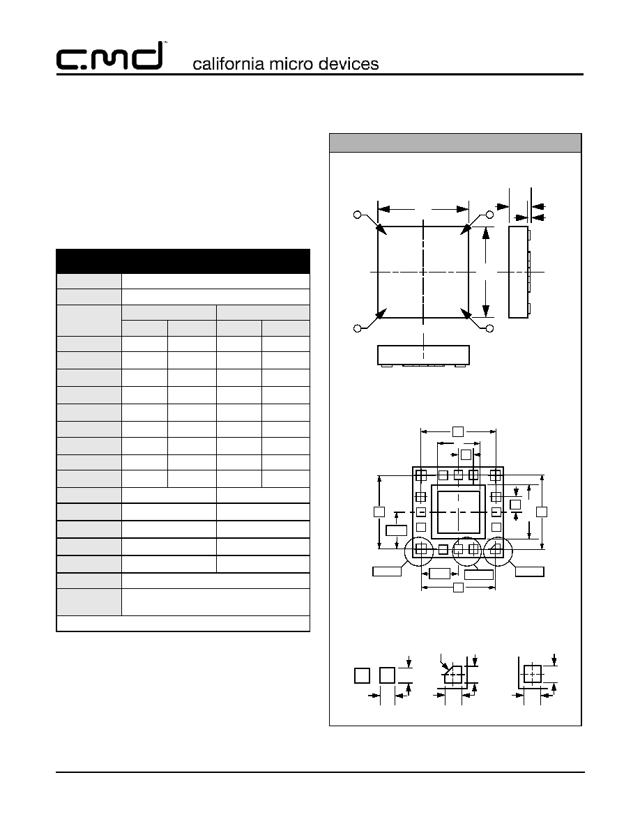
Mechanical Details
The CM2400-02/03/04 family is available in a 16-lead
HBCC and 16-lead TSSOP packages.The mechanical
details for these packages are presented below.
HBCC-16 Mechanical Specifications
Dimensions for the CM2400-02HB, CM2400-03HB and
CM2400-04HB devices packaged in 16-pin HBCC
packages are presented below.
* This is an approximate number which may vary.
Dimensions for HBCC-16 Package
PACKAGE DIMENSIONS
Package
HBCC-16
Pins
16
Dimensions
Millimeters
Inches
Min
Max
Min
Max
A
-
0.80
0.0315
A
1
0.05
0.10
0.0039
b
1
0.25
0.35
0.0138
b
2
0.30
0.40
0.0157
b
3
0.30
0.40
0.0157
D
2.90
3.10
0.1220
D
h
1.45
1.55
0.0610
E
2.90
3.10
0.1220
E
h
1.75
1.85
0.0728
e
0.50 TYP.
0.0197 TYP.
e
1
2.50 TYP.
0.0984 TYP.
e
2
2.50 TYP.
0.0984 TYP.
e
3
2.45 TYP.
0.0965 TYP.
e
4
2.45 TYP
0.0965 TYP.
# per tube
120 pieces*
# per tape
and reel
2500 pieces
Controlling dimension: millimeters
b
1
b
1
Detail A
Mechanical Package Diagrams
BOTTOM VIEW
TOP VIEW
SIDE VIEW
CONTACT (PIN) DIMENSIONS
b
3
b
3
b
2
CF#0.20x45
b
2
Detail C
Detail B
E
D
5
9
1
13
A
A
1
e
2
E
h
e
D
h
e
3
e
1/2
e
4
1/2
e
3
5
1
13
9
16
e
4
Detail B
e
1
Detail C
Detail A

©
2004 California Micro Devices Corp. All rights reserved.
14
430 N. McCarthy Blvd., Milpitas, CA 95035-5112
Tel: 408.263.3214
Fax: 408.263.7846
www.calmicro.com
08/24/04
CM2400-02/03/04
PRELIMINARY
Mechanical Details (cont'd)
TSSOP-16 Mechanical Specifications
Dimensions for the CM2400-02TS and CM2400-03TS
devices packages are presented below.
For complete information on the TSSOP-16 package,
see the California Micro Devices TSSOP Package
Information document.
Dimensions for the TSSOP-16 Package
PACKAGE DIMENSIONS
Package
TSSOP
Pins
16
Dimensions
Millimeters
Inches
Min
Max
Min
Max
A
--
1.10
--
0.0433
A1
0.05
0.15
0.002
0.006
B
0.19
0.30
0.0075
0.0118
C
0.09
0.20
0.0035
0.0079
D
4.90
5.10
0.193
0.201
E
4.30
4.50
0.169
0.177
e
0.65 BSC
0.0256 BSC
H
6.25
6.50
0.246
0.256
L
0.50
0.70
0.020
0.028
# per tube
Consult Factory
# per tape
and reel
2500 pcs
Controlling dimension: millimeters
Mechanical Package Diagrams
E
D
H
TOP VIEW
L
END VIEW
C
e
B
A
A1
SEATING
PLANE
SIDE VIEW
5
6
7
8
1
2
3
4
12
11
10
9
16
15
14
13
Pin 1 Marking