
©
2004 California Micro Devices Corp. All rights reserved.
06/30/04
430 N. McCarthy Blvd., Milpitas, CA 95035-5112
Tel: 408.263.3214
Fax: 408.263.7846
www.calmicro.com
1
CM2400-05
PRELIMINARY
Universal Serial Bus Transceiver with Level Translator
Features
∑
Complies with USB Specification Rev 1.1 & 2.0
∑
Supports Full Speed Mode (12Mbit/s)
∑
Integrated 5V to 3.3V regulator
∑
Bi-directional driver input/output pins
∑
Two single-ended receivers with hysteresis
∑
USB detection of V
BUS
via level translator
∑
Stable RCV output during SE0 condition
∑
Low power operation
∑
Supports 1.65 to 3.6V I/O voltage levels
∑
Full industrial operating range -40 to 85
∞
C
∑
Available in tiny HBCC-16 and TQFN-16 packages
∑
Lead-free versions available
Applications
∑
Wireless Handsets
∑
Digital Still Cameras
∑
PDAs (Personal Digital Assistants)
∑
IAs (Information Appliances)
∑
Pin and functionally compatible with Philips
ISP1102
Product Description
The CM2400-05 Universal Serial Bus (USB) trans-
ceiver is fully compliant with USB specification, revi-
sions 1.1 and 2.0. It supports a speed of 12Mbits/s
(Full Speed Mode).
An internal level shifter allows interface to Application
Specific Integrated Circuits (ASICs) and Programma-
ble Logic Devices (PLDs) running at core voltages of
1.65V to 3.6V.
An internal 5V to 3.3V regulator is used to power the
CM2400-05 USB transceiver via the USB supply V
BUS
.
V
M
/V
MO
and V
P
/V
PO
are bi-directional interface pins. In
one mode they function as the differential driver input
data. In another mode they function as the output of
the single ended receivers. This mode is configured by
the OE pin.
This device is ideal for portable electronic devices such
as mobile phones, digital still cameras, PDAs (Personal
Digital Assistants) and IAs (Information Appliances).
The CM2400-05 is manufactured in small form-factor
16-lead HBCC or TQFN packages to conserve board
space and is available with optional lead-free finishing.
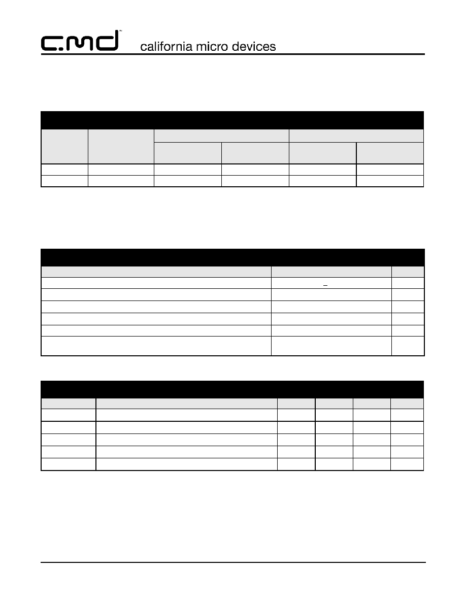
Simplified Block Schematic
Voltage
Detector
Voltage
Regulator
V
CC
USB_DET
ENUM
OE
SPND
V
M
/V
MO
*
RCV
GND
D-
D+
V
PU
V
REG
V
BUS
ENABLE
V
P
/V
PO
*
LEVEL TRANSLA
T
OR
* Pins are bi-directional based on OE state:
If OE = V
CC
, then V
M
/V
MO
and V
P
/V
PO
are configured as outputs.
If OE = GND, then V
M
/V
MO
and V
P
/V
PO
are configured as inputs.

©
2004 California Micro Devices Corp. All rights reserved.
2
430 N. McCarthy Blvd., Milpitas, CA 95035-5112
Tel: 408.263.3214
Fax: 408.263.7846
www.calmicro.com
06/30/04
CM2400-05
PRELIMINARY
PIN DESCRIPTIONS
PINS
NAME
DESCRIPTION
1
OE
Input for Output Enable (Active low). Enables transceiver driver to transmit data on the USB bus. When
OE pin = LOW, driver circuitry is enabled.
2
RCV
Differential receiver output of D+ and D- input data lines. The output state of RCV is preserved and sta-
ble during an SE0 condition.
3
V
P
/V
PO
Bi-directional input output of D+. Configured by OE.
4
V
M
/V
MO
Bi-directional input output of D-. Configured by OE.
5
SPND
Suspend input. Allows the device to enter a low power state while the USB is inactive.
6
N.C.
No internal connection to circuitry.
7
V
CC
Supply voltage for digital I/O pins. Voltages supported: 1.65 to 3.3V.
8
USB_DET
I/O level USB detect output. Logic High indicates that a USB cable is present.
9
D-
Negative USB data connection.
10
D+
Positive USB data connection. In full-speed connect mode, connect to V
PU
via a 1.5k
resistor. Toler-
ance of this resistor is defined in the USB specification REV 1.1 & 2.0
11
N.C.
No internal connection to circuitry.
12
N.C.
No internal connection to circuitry.
13
V
REG
Regulated supply voltage output during USB operation of V
BUS
. 1
µF decoupling capacitor is required.
14
V
BUS
Supply voltage input. Can be directly connected to USB V
BUS
.
15
V
PU
Pull-up supply voltage. Pin function is controlled by input ENUM.
16
ENUM
Enumerate, allows software to control connection of the external pull-up via the level translator. If
ENUM = LOW then V
PU
is floating. If ENUM = HIGH then V
PU
is internally connected to V
REG
.
17
GND
The ground terminal is connected to the exposed diepad (heatsink)
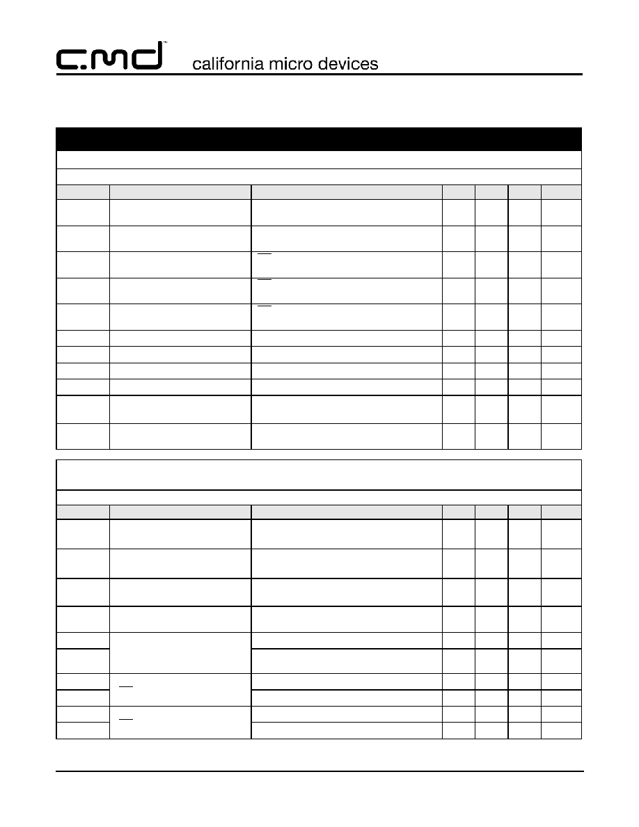
PACKAGE / PINOUT DIAGRAM
Note: This drawing is not to scale.
Bottom View
HBCC16 Package
5
4
3
2
1
16
15 14
6
7
8
10
11
12
9
13
GND
HBCC-16
17
SPND
V
M
/V
MO
V
P
/V
PO
RCV
OE
ENUM
V
BU
S
V
PU
V
REG
N.C.
N.C.
D+
D-
USB_DET
V
CC
N.C
.
4
3
2
1
9
10
11
12
5
6
7
8
16 15 14 13
TQFN-16
V
M
/V
MO
V
P
/V
PO
RCV
OE
D-
D+
N.C.
N.C.
SPND
N.C
.
V
CC
USB_DET
ENUM
V
PU
V
BU
S
V
REG
Bottom View
TQFN16 Package
GND
17
©
2004 California Micro Devices Corp. All rights reserved.
06/30/04
430 N. McCarthy Blvd., Milpitas, CA 95035-5112
Tel: 408.263.3214
Fax: 408.263.7846
www.calmicro.com
3
CM2400-05
PRELIMINARY
Ordering Information
Note 1: There is one additional GND pad on the bottom of the device not included in this pin count.
Note 2: Parts are shipped in Tape & Reel form unless otherwise specified.
Note 3: Lead-free, 100% tin plated.
Specifications
Note 1: Equivalent to discharging a 100pF capacitor via a 1.5k
resistor (Human Body Model).
PART NUMBERING INFORMATION
Pads/Pins
1
Package
Standard Finish
Lead-free Finish
3
Ordering Part
Number
2
Part Marking
Ordering Part
Number
2
Part Marking
16
HBCC-16
CM2400-05HB
CM240 005HB
CM2400-05HA
CM240 005HA
16
TQFN-16
CM2400-05QF
CM240 005QF
CM2400-05QE
CM240 005QE
ABSOLUTE MAXIMUM RATINGS
PARAMETER
RATING
UNITS
ESD Protection (HBM, All Pins, See Note 1)
+2000
V
V
BUS
[GND - 0.5] to +5.5
V
V
CC
[GND - 0.5] to +6.0
V
V
I
(INPUT)
[GND - 0.5] to [V
CC
+ 0.5]
V
Storage Temperature Range
-40 to +150
∞C
Operating Temperature Range
Junction
-40 to +150
∞C
STANDARD (RECOMMENDED) OPERATING CONDITIONS
SYMBOL
PARAMETER
MIN
TYP
MAX
UNITS
V
BUS
USB V
BUS
Supply
4.1
5.0
5.5
V
V
CC
DC System Supply
1.65
3.3
3.6
V
V
I
DC Input Voltage
0
-
V
CC
V
V
I(AI/O)
Analog I/O Pins (D+, D-)
0
-
3.6
V
T
A
Ambient Operating Temperature Range
-40
-
85
∞C

©
2004 California Micro Devices Corp. All rights reserved.
4
430 N. McCarthy Blvd., Milpitas, CA 95035-5112
Tel: 408.263.3214
Fax: 408.263.7846
www.calmicro.com
06/30/04
CM2400-05
PRELIMINARY
Specifications (cont'd)
Note 1: Operating Characteristics are over Standard Operating Conditions unless otherwise specified.
Note 2: Excluding any load current and V
PU
/V
SW
source current to 1.5k
and 15k pull-up and pull-down resistors (200
µ
A).
ELECTRICAL OPERATING CHARACTERISTICS
(SEE NOTE 1)
Static Operating Characteristics
Supply Pins (V
BUS
= 4.1V to 5.5V; V
CC
= 1.65V to 3.6V)
SYMBOL
PARAMETER
CONDITIONS
MIN
TYP
MAX
UNITS
V
REG
Regulated supply output
Unloaded
3.0
3.3
3.6
V
I
BUS
Operating supply current
Full-speed TX and RX;
C
L
=50pF on
D+/D- outputs
10
mA
I
BUS(IDLE)
Supply current during full
speed idle and SE0
Full-speed idle; Note 2
500
µ
A
I
BUS(SUSP)
Supply current during sus-
pend
SPND = logic "1"; Note 2
100
µ
A
I
CC
Operating I/O supply current
Full-speed TX and RX
2.0
mA
I
CC(STAT)
Static I/O supply current
Full-speed idle, SE0 or suspend
10.0
µ
A
I
CC(SHARE)
Supply current during shar-
ing mode
V
BUS
not connected
10.0
µ
A
I
DX(SHARE)
D+/D- load current during
sharing mode
V
BUS
not connected;
ENUMERATE = logic "0"
10.0
µ
A
V
TH(VBUS)
V
BUS
supply detection
threshold, USB_D output
Supply lost (USB_D low)
3.6
V
Supply present
4.1
V
V
TH(BUS)
Hysteresis
100
mV
V
TH(VCC)
V
CC
supply detection
threshold.
Supply lost
0.5
V
Supply present
1.4
V
V
TH(VCC)
Hysteresis
200
mV
Digital Pins (V
BUS
= 4.1V to 5.5V; V
CC
= 1.65V to 3.6V)
SYMBOL
PARAMETER
CONDITIONS
MIN
TYP
MAX
UNITS
V
IL
Logic LOW input voltage
0.3 X V
CC
V
V
IH
Logic HIGH input voltage
0.6 X V
CC
V
V
OL
Logic LOW output voltage
I
OL
= 100
µA
I
OL
= 2mA
0.15
0.40
V
V
V
OH
Logic HIGH output voltage
I
OH
= 100
µA
I
OH
= 2mA
V
CC
- 0.15
V
CC
- 0.40
V
V
©
2004 California Micro Devices Corp. All rights reserved.
06/30/04
430 N. McCarthy Blvd., Milpitas, CA 95035-5112
Tel: 408.263.3214
Fax: 408.263.7846
www.calmicro.com
5
CM2400-05
PRELIMINARY
Specifications (cont'd)
Note 3: Rev 2.0 states Z
DRV
must be between 28
and 44, when the driver is not high speed capable.
ELECTRICAL OPERATING CHARACTERISTICS (CONT'D)
Static Operating Characteristics (cont'd)
Analog I/O Pins (V
BUS
= 4.1V to 5.5V; V
CC
= 1.65V to 3.6V)
SYMBOL
PARAMETER
CONDITIONS
MIN
TYP
MAX
UNITS
V
DI
Differential receiver input sensi-
tivity
|
V
I
(D+) - V
I
(D-)
|
0.2
V
V
CM
Differential receiver
common mode voltage
0.8
2.5
V
V
IL
Single-ended receiver
logic LOW input voltage
OE = logic "1"
0.8
V
V
IH
Single-ended receiver
logic HIGH input voltage
OE = logic "1"
2.0
V
V
HYS
Single-ended receiver
Hysteresis voltage
OE = logic "1"
0.4
0.7
V
V
OL
Logic LOW output voltage
R
L
= 1.5k
tied to +3.6V
0.3
V
V
OH
Logic HIGH output voltage
R
L
= 15k
tied to GND
2.8
3.6
V
I
LZ
OFF-state leakage current
±1
µ
A
C
IN
Transceiver Capacitance
Pin to GND
10
pF
R
SW
Internal switch resistance at
V
PU
30
Z
DRV
Driver output impedance
(includes 33 ohm 1% resistor)
Measured with steady-state drive; See Note
3
33
39
44
Dynamic Operating Characteristics:
Analog I/O Pins (VBUS = 4.1 to 5.5V; VCC = 1.65 to 3.6V)
Driver Characteristics & Timings (Full-speed mode only)
SYMBOL
PARAMETER
CONDITIONS
MIN
TYP
MAX
UNITS
t
FR
Rise time
C
L
= 50 to 125pF, measured 10% to 90%
(V
OH
-V
OL
); See
Figure 6
4
20
ns
t
FF
Fall time
C
L
= 50 to 125pF, measured 10% to 90%
(V
OH
-V
OL
); See
Figure 6
4
20
ns
FRFM
Differential rise / fall time match-
ing (t
FR
/t
FF
)
Excluding the first transition from idle state
90
110
%
V
CRS
Output signal crossover
voltage
Excluding the first transition from idle state;
See
Figure 9
1.3
2.0
V
t
PLH(DRV)
Driver propagation delay (V
O
/
V
PO
D+/D-, FSEO/V
MO
D+/D-
LOW-to-HIGH transition; See
Figure 9
18
ns
t
PHL(DRV)
HIGH-to-LOW transition; See
Figure 9
18
ns
t
PHZ
Driver disable delay
(OE
D+/D-)
HIGH-to-OFF; See
Figure 7
18
ns
t
PLZ
LOW-to-OFF; See
Figure 7
18
ns
t
PZH
Driver enable delay
(OE
D+/D-)
OFF-to-HIGH; See
Figure 7
15
ns
t
PZL
OFF-to-LOW; See
Figure 7
15
ns