 | –≠–ª–µ–∫—Ç—Ä–æ–Ω–Ω—ã–π –∫–æ–º–ø–æ–Ω–µ–Ω—Ç: CM3002-33 | –°–∫–∞—á–∞—Ç—å:  PDF PDF  ZIP ZIP |
©
2004 California Micro Devices Corp. All rights reserved.
08/16/04
430 N. McCarthy Blvd., Milpitas, CA 95035-5112
Tel: 408.263.3214
Fax: 408.263.7846
www.calmicro.com
1
CM3002
Micropower 1.0A Low Dropout CMOS Regulators
Features
∑
Regulated output options: 1.5, 1.8, 2.5 and
3.3 volts
∑
1.0A output current
∑
Operates from 3.3V supply (5.0V for CM3002-33)
∑
Very low dropout voltage on CM3002-33
products (500mV@1A)
∑
Enable Output Control for power-up sequencing
∑
Low quiescent operating current (< 600
µ
A typical)
∑
Current limit protection
∑
Thermal overload protection
∑
Reverse voltage protection
∑
Available in thermally-enhanced SOIC-8 and
MSOP-8 (CM3002-33MA/MF) packages
∑
Lead-free versions available
Applications
∑
Low Voltage "Core" Processors
∑
Peripheral Adapter Cards
∑
Portable/Battery-Powered Devices
Product Description
The CM3002 family of regulators are very low dropout
regulators that deliver up to 1.0A of load current at a
fixed voltage output. Input and output voltage options
for the CM3002 family devices are presented in
Table 1
.
Operating from a single input supply, these devices are
ideally suited for powering low voltage "core" proces-
sors, especially where a 3.3V source is already avail-
able.
These regulators feature a dedicated control input (EN,
Active High) for power-up sequencing flexibility. When
this input is taken low, the regulator output is disabled.
In this state, the supply current will drop to a low level
to ensure all the internal control circuitry still remains
active. This provides excellent start-up response when-
ever the device comes out of shutdown.
The CM3002 family of regulators is fully protected,
offering both overload current limiting and high temper-
ature thermal shutdown. Housed in space saving ther-
mally-enhanced SOIC-8 and MSOP-8 (CM3002-33MA/
MF) packages, these devices ensure maximum junc-
tion-to-ambient power dissipation.
The CM3002 is available with optional lead-free finish-
ing.
Table 1: CM3002 Regulator Family
PRODUCT
INPUT
VOLTAGE
OUTPUT VOLTAGE
CM3002-15SA/SF
3.3V
1.5V
CM3002-18SA/SF
3.3V
1.8V
CM3002-25SA/SF
3.3V
2.5V
CM3002-33SA/SF
5.0V or 3.3V
3.3V
CM3002-33MA/MF
5.0V or 3.3V
3.3V
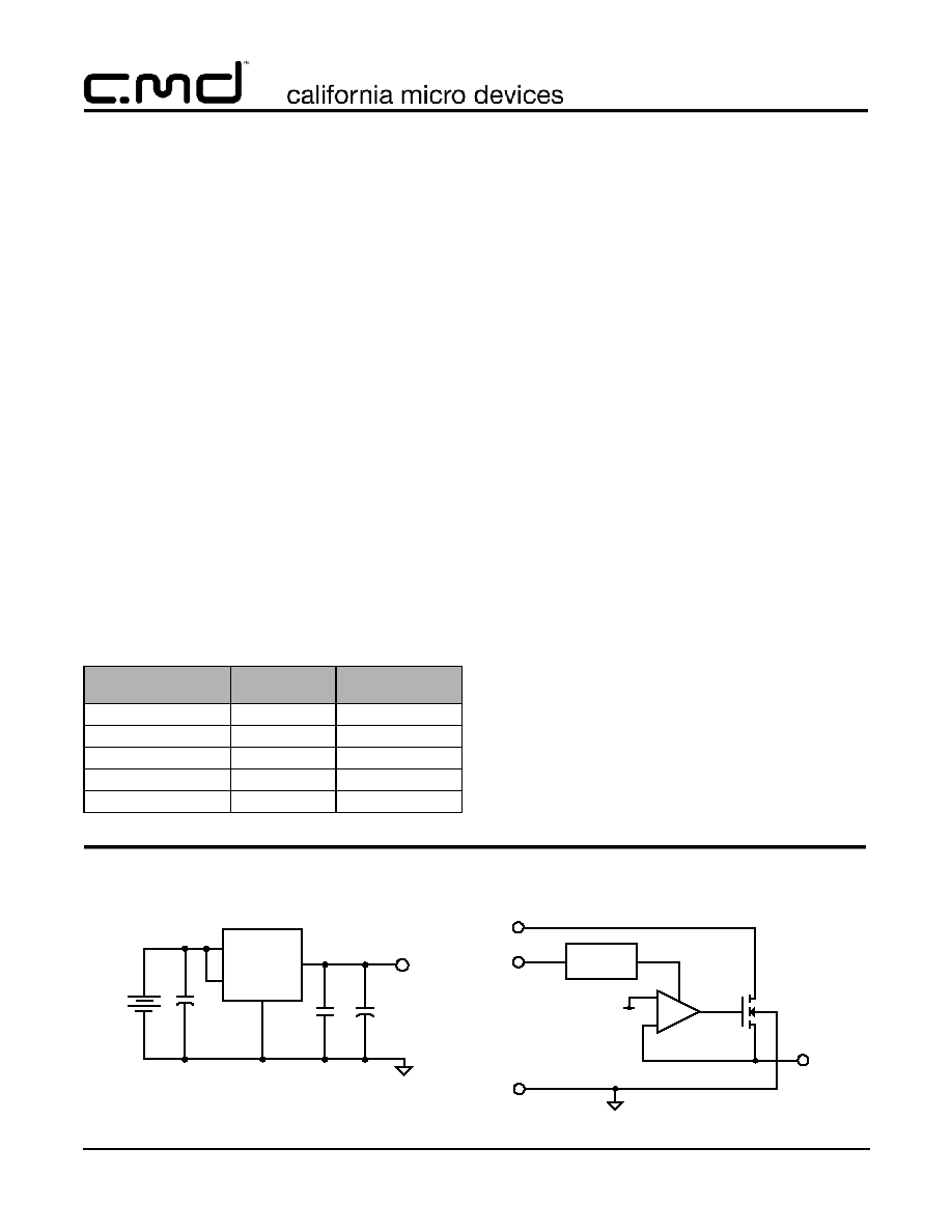
Simplified Electrical Schematic
Typical Application Circuit
EN
Reference
Voltage
+
V
CC
GND
EN
V
OUT
Thermal Sensor
&
Current Limit
-
V
CC
EN
V
OUT
GND
Supply
Voltage
1
µ
F
100nF
10
µ
F
+
-
V
OUT
+
+
©
2004 California Micro Devices Corp. All rights reserved.
2
430 N. McCarthy Blvd., Milpitas, CA 95035-5112
Tel: 408.263.3214
Fax: 408.263.7846
www.calmicro.com
08/16/04
CM3002
Ordering Information
Note 1: Parts are shipped in Tape & Reel form unless otherwise specified.
PIN DESCRIPTIONS
PIN(S)
NAME
DESCRIPTION
1
EN
A logic input control to enable the regulator output. When EN is asserted (logic high), it allows out-
put regulation to commence. When EN is deasserted (logic low), the regulator pass transistor (N-
channel MOSFET) is forced into a high impedance mode.
All other internal circuitry is unaffected by the state of the EN input and will always remain powered
whenever V
CC
is present.
An internal pull-up current (2
µA) from V
CC
must be overdriven in order to apply a Logic Low to the
EN control input.
The EN control input is intended to be used for power-up sequencing.
2
V
CC
The input power supply for the regulator. If this input is within a few inches of the main supply filter,
a capacitor may not be necessary. Otherwise an input filter capacitor of approximately 1uF to 10uF
will ensure adequate filtering.
3
V
OUT
The regulator voltage output used to power the load. A nominal output capacitor of 10uF is suffi-
cient to minimize any transient disturbances under normal operating conditions. Additional output
capacitance can be used to further improve transient load response.
4
N.C.
These pins have no connection to the internal device. To provide additional thermal performance,
these pins can be connected directly to the PC board GND plane.
5,6,7,8
GND
The negative reference for all voltages.
PACKAGE / PINOUT DIAGRAMS
8-pin SOIC
Top View
1
2
3
4
8
7
6
5
EN
V
CC
V
OUT
N.C.
GND
GND
GND
GND
Note: These drawings are not to scale.
8-pin MSOP
Top View
1
2
3
4
8
7
6
5
EN
V
CC
V
OUT
N.C.
GND
GND
GND
GND
(CM3002-33MA/MF only)
(CM3002-xxSA/SF)
PART NUMBERING INFORMATION
Regulator
Pins
Package
Standard Finish
Lead-free Finish
Ordering Part
Number
1
Part Marking
Ordering Part
Number
1
Part Marking
CM3002-15
8
Power SOIC
CM3002-15SA
CM3002-15SA
CM3002-15SF
CM3002-15SF
CM3002-18
8
Power SOIC
CM3002-18SA
CM3002-18SA
CM3002-18SF
CM3002-18SF
CM3002-25
8
Power SOIC
CM3002-25SA
CM3002-25SA
CM3002-25SF
CM3002-25SF
CM3002-33
8
Power SOIC
CM3002-33SA
CM3002-33SA
CM3002-33SF
CM3002-33SF
CM3002-33
8
Power MSOP
CM3002-33MA
233
CM3002-33MF
233R
©
2004 California Micro Devices Corp. All rights reserved.
08/16/04
430 N. McCarthy Blvd., Milpitas, CA 95035-5112
Tel: 408.263.3214
Fax: 408.263.7846
www.calmicro.com
3
CM3002
Specifications
Note 1: The SOIC and MSOP packages are thermally enhanced through the use of a fused integral leadframe. The power rating is
based on a printed circuit board heat spreading capability equivalent to 2 square inches of copper connected to the GND
pins. Typical multi-layer boards using power plane construction will provide this heat spreading ability without the need for
additional dedicated copper area. Please consult with factory for thermal evaluation assistance.
ABSOLUTE MAXIMUM RATINGS
PARAMETER
RATING
UNITS
ESD Protection (HBM)
+2000
V
Pin Voltages
V
CC
EN
V
OUT
[GND - 0.4] to [+6.0]
[GND - 0.4] to [+6.0]
[GND - 0.4] to [+6.0]
V
V
V
Storage Temperature Range
-40 to +150
∞C
Operating Temperature Range
Ambient
Junction
0 to +70
0 to +150
∞C
∞C
Power Dissipation (Note 1)
Internally Limited
W
STANDARD OPERATING CONDITIONS
PARAMETER
RATING
UNITS
V
CC
(CM3002-15SA, CM3002-18SA, CM3002-25SA)
3.0 to 3.6
V
V
CC
(CM3002-33SA, CM3002-33MA)
3.0 to 5.5
V
Ambient Operating Temperature Range
0 to +70
∞C
Load Current
0 to +1000
mA
C
EXT
10 +20%
µ
F
©
2004 California Micro Devices Corp. All rights reserved.
4
430 N. McCarthy Blvd., Milpitas, CA 95035-5112
Tel: 408.263.3214
Fax: 408.263.7846
www.calmicro.com
08/16/04
CM3002
Specifications (cont'd)
Note 1: Operating Characteristics are over Standard Operating Conditions unless otherwise specified.
ELECTRICAL OPERATING CHARACTERISTICS
(SEE NOTE 1)
SYMBOL
PARAMETER
CONDITIONS
MIN
TYP
MAX
UNITS
V
OUT
Regulator Output Voltage
CM3002-15SA/SF
CM3002-18SA/SF
CM3002-25SA/SF
CM3002-33SA/SF, -33MA/MF
0mA < I
LOAD
< 1000mA
0mA < I
LOAD
< 1000mA
0mA < I
LOAD
< 1000mA
0mA < I
LOAD
< 1000mA; V
CC
=5.0
1.42
1.72
2.40
3.10
1.50
1.80
2.50
3.30
1.58
1.88
2.60
3.50
V
V
V
V
I
LIM
Overload Current Limit
1500
mA
V
R LOAD
Load Regulation
CM3002-15SA/SF, -18SA/SF,
-25SA/SF
CM3002-33SA/SF, -33MA/MF
10mA < I
LOAD
< 1000mA; V
CC
=3.3V
10mA < I
LOAD
< 1000mA; V
CC
=5.0V
20
20
mV
mV
V
R LINE
Line Regulation
xx
CM3002-15SA/SF
I
LOAD
= 5mA; 3.0V < V
CC
< to 5.5V
20
mV
CM3002-18SA/SF
I
LOAD
= 5mA; 3.0V < V
CC
< to 5.5V
20
mV
CM3002-25SA/SF
I
LOAD
= 5mA; 3.0V < V
CC
< to 5.5V
30
mV
CM3002-33SA/SF, -33MA/MF
I
LOAD
= 5mA; 4.5V < V
CC
< to 5.5V
20
mV
I
Q
Quiescent Current
CM3002-15SA/SF
EN tied to V
CC
; I
LOAD
= 0mA
500
900
µ
A
CM3002-18SA/SF
EN tied to V
CC
; I
LOAD
= 0mA
500
900
µ
A
CM3002-25SA/SF
EN tied to V
CC
; I
LOAD
= 0mA
500
900
µ
A
CM3002-33SA/SF, -33MA/MF
EN tied to V
CC
; I
LOAD
= 0mA
600
900
µ
A
I
Q
Quiescent Current
CM3002-15SA/SF
EN tied to GND; I
LOAD
= 0mA
150
300
µ
A
CM3002-18SA/SF
EN tied to GND; I
LOAD
= 0mA
150
300
µ
A
CM3002-25SA/SF
EN tied to GND; I
LOAD
= 0mA
150
300
µ
A
CM3002-33SA/SF, -33MA/MF
EN tied to GND; I
LOAD
= 0mA
200
300
µ
A
I
GND
Ground Current
CM3002-15SA/SF
I
LOAD
= 0mA
500
900
µ
A
CM3002-18SA/SF
I
LOAD
= 0mA
500
900
µ
A
CM3002-25SA/SF
I
LOAD
= 0mA
500
900
µ
A
CM3002-33SA/SF, -33MA/MF
I
LOAD
= 0mA
600
900
µ
A
I
GND
Ground Current
CM3002-15SA/SF
I
LOAD
= 1000mA
500
900
µ
A
CM3002-18SA/SF
I
LOAD
= 1000mA
500
900
µ
A
CM3002-25SA/SF
I
LOAD
= 1000mA
500
900
µ
A
CM3002-33SA/SF, -33MA/MF
I
LOAD
= 1000mA
600
900
µ
A
I
RCC
V
CC
Pin Reverse Leakage
V
OUT
= 3.3V; V
CC
= 0V
1
100
µA
V
IH
Enable Input Logic High Threshold
1.5
V
V
IL
Enable Input Logic Low Threshold
0.3
V
I
EN
Enable Input Current
Internal current source from V
CC
2
10
µ
A
T
DISABLE
Shutdown Temperature
160
∞C
T
HYST
Thermal Hysteresis
25
∞C

©
2004 California Micro Devices Corp. All rights reserved.
08/16/04
430 N. McCarthy Blvd., Milpitas, CA 95035-5112
Tel: 408.263.3214
Fax: 408.263.7846
www.calmicro.com
5
CM3002
Performance Information
CM3002-15SA/SF Typical DC Characteristics (nominal conditions unless specified otherwise)
Supply Current vs. Voltage (EN=VCC)
Supply Current vs. Voltage (EN=GND)
Line Regulation with 1A Load
Load Regulation
Ground Current vs. Output Load
0
100
200
300
400
500
600
700
0
1
2
3
4
5
VCC [V]
V
Supply
Current
[
uA]
0
100
200
300
400
500
600
700
0
1
2
3
4
5
Supply
C
urrent
[uA]
1.42
1.44
1.46
1.48
1.50
1.52
1.54
1.56
1.58
3.0
3.1
3.2
3.3
3.4
3.5
3.6
V
OUT
[V]
0
100
200
300
400
500
600
700
0
200 400 600 800 1000 1200
Ground
Current
[uA]
1.42
1.44
1.46
1.48
1.50
1.52
1.54
1.56
1.58
0
200 400 600 800 1000 1200
V
OUT
[V]
VCC [V]
Load Current [mA]
Current Limiting Protection
0.0
0.2
0.4
0.6
0.8
1.0
1.2
1.4
1.6
0
500
1000
1500
2000
V
OUT
[V]
Load Current [mA]
Load Current [mA]
VCC [V]