© 2004 California Micro Devices Corp. All rights reserved.
01/15/04
430 N. McCarthy Blvd., Milpitas, CA 95035-5112
L Tel: 408.263.3214 L Fax: 408.263.7846 L www.calmicro.com
1
CM3003
1.5 Amp Dual Mode Low Dropout CMOS Regulator
Features
∑
Adjustable Output or Internally Fixed
∑
375mV dropout at 1.5A load current
∑
Operates from 2.2V to 5.5V input supply
∑
Low Ground current (330
µA at 1.5A Load)
∑
Minimal output capacitance required
∑
Current Limit Protection
∑
Thermal Overload Protection
∑
Reverse Voltage Protection
∑
Thermally enhanced 8-pin SOIC package
∑
Lead-free versions available
Applications
∑
Low Voltage "Core" processors
∑
Graphics Cards
∑
Gigabit NIC Cards
∑
PC Motherboards
∑
Notebooks
Product Description
The CM3003 is a family of very low dropout regulators
that offers dual mode operation. When the Adjust con-
trol pin (ADJ) is grounded, these devices automatically
enter a fixed voltage mode and deliver either a 1.8V or
2.5V output capable of supplying 1.5A, depending on
the device utilized. When the Adjust pin is connected to
an external resistor network the device automatically
operates as an adjustable regulator. The Adjust pin can
also be tied directly to the OUT pin which configures
the CM3003 as a 1.2V regulator.
An Enable control pin (EN) allows the device to be
placed in a low current mode.
The CM3003 devices are fully protected, offering both
overload current limiting, short circuit protection and
high temperature thermal shutdown. These devices
also includes reverse voltage protection that minimizes
any reverse current flow back into the output pin.
The CM3003 devices are housed in a space saving, 8-
pin power SOIC packages which has been thermally
enhanced (integral leadframe) to ensure maximum
junction to ambient power dissipation.
The CM3003 devices are available with optional lead-
free finishing.
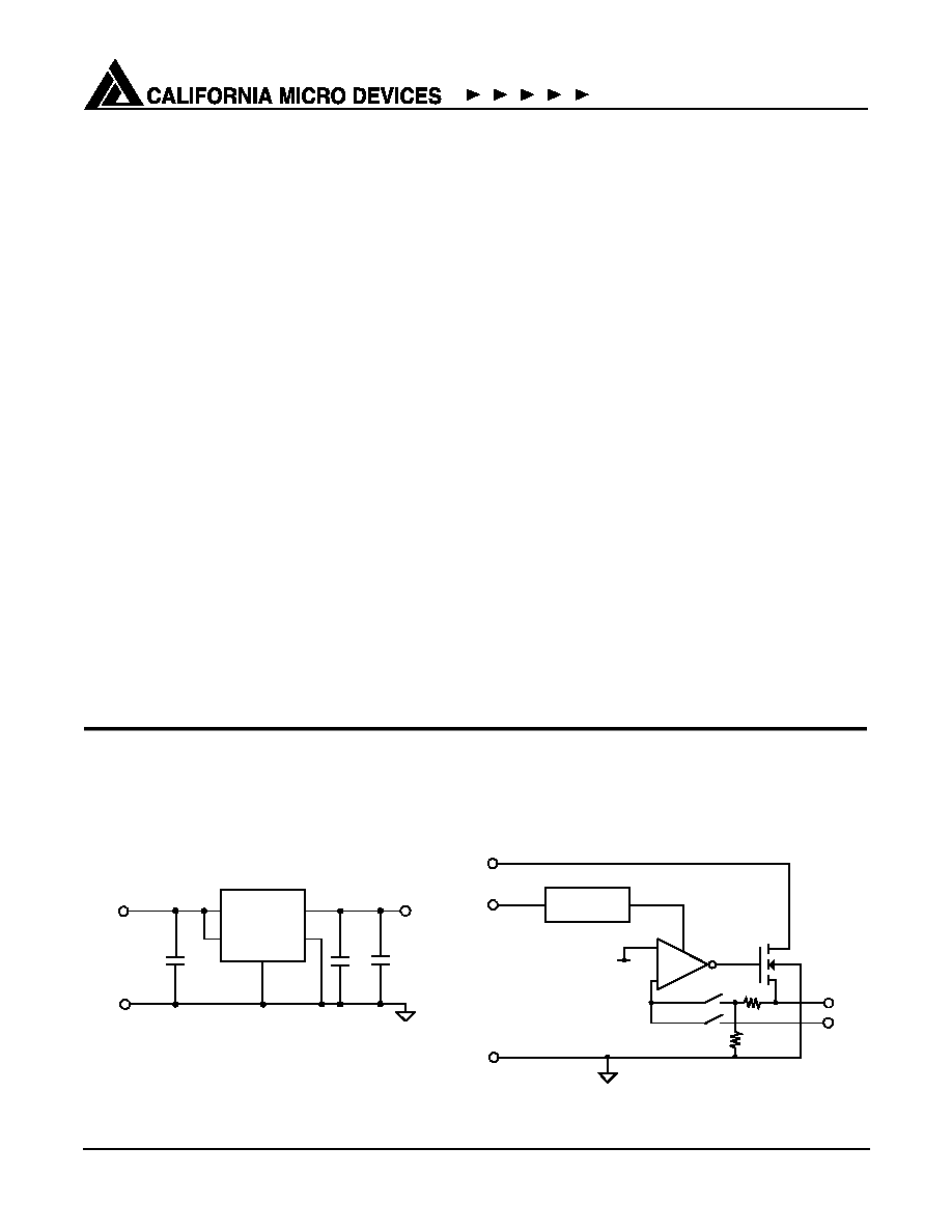
Simplified Electrical Schematic
Typical Application Circuit
IN
EN
OUT
GND
10
µ
F
100
n
F
V
OUT
GND
CM3003
ADJ
V
IN
2.2V - 5.5V
10
µ
F
1.8V/2.5V@1.5A
EN
1.2V Reference
Voltage
+
IN
GND
EN
ADJ
Over Current
Short Circuit
Over Temp
-
2.2V-5.5V
Controller
2.5V Output when ADJ = GND
OUT
Automatically selects Adjustable Output
(when external resistors are present)
Fixed
Adj
130K
120K
1.5 AMP

© 2004 California Micro Devices Corp. All rights reserved.
2
430 N. McCarthy Blvd., Milpitas, CA 95035-5112
L Tel: 408.263.3214 L Fax: 408.263.7846 L www.calmicro.com
01/15/04
CM3003
Ordering Information
Note 1: Parts are shipped in Tape & Reel form unless otherwise specified.
PIN DESCRIPTIONS
PIN(S)
NAME
DESCRIPTION
1
EN
Enable/shutdown input. When EN is asserted high (V
EN
1.2V), the regulator is enabled. When EN
is asserted low (V
EN
0.4V), the regulator is shut down.
2
IN
Positive input voltage for the regulator. If this input pin is greater than 2 inches from the main input
filter, a 10
µF ceramic capacitor is recommended for adequate filtering.
3
OUT
The regulated voltage output. An output capacitor of 10
µF is recommended to minimize any tran-
sient load disturbances under normal operating conditions. Additional output capacitance can be
used to further improve transient load response.
4
ADJ
Feedback input. When ADJ is grounded, the device enters fixed voltage mode. When ADJ is con-
nected to an external resistor network, the device operates as an adjustable regulator. The Adjust
pin can also be tied directly to the OUT pin which configures the CM3003 as a 1.2V regulator.
5-8
GND
The negative reference for all voltages. Also functions as a thermal path for heat dissipation.
PACKAGE / PINOUT DIAGRAM
Note: This drawing is not to scale.
8-pin Power SOIC
1
2
3
4
8
7
6
5
EN
IN
OUT
ADJ
GND
GND
GND
GND
TOP VIEW
PART NUMBERING INFORMATION
Pins
Output Voltage
Package
Standard Finish
Lead-free Finish
Ordering Part
Number
1
Part Marking
Ordering Part
Number
1
Part Marking
8
2.5
SOIC-8
CM3003-25SA
CM3003-25SA
CM3003-25SF
CM3003-25SF
8
1.8
SOIC-8
CM3003-18SA
CM3003-18SA
CM3003-18SF
CM3003-18SF
© 2004 California Micro Devices Corp. All rights reserved.
01/15/04
430 N. McCarthy Blvd., Milpitas, CA 95035-5112
L Tel: 408.263.3214 L Fax: 408.263.7846 L www.calmicro.com
3
CM3003
Specifications
Note 1: The SOIC package used is thermally enhanced through the use of a fused integral leadframe. The power rating is based on
a printed circuit board heat spreading capability equivalent to 2 square inches of copper connected to the GND pins. Typical
multi-layer boards using power plane construction will provide this heat spreading ability without the need for additional ded-
icated copper area. (Please consult with factory for thermal evaluation assistance)
ABSOLUTE MAXIMUM RATINGS
PARAMETER
RATING
UNITS
ESD Protection (HBM)
±2000
V
Pin Voltages
IN, OUT, ADJ, EN
[GND - 0.4] to +6.0
V
Storage Temperature Range
-40 to +150
∞C
Operating Temperature Range
Ambient
Junction
-40 to +85
-40 to +150
∞C
∞C
Power Dissipation (See note 1)
Internally Limited
W
STANDARD OPERATING CONDITIONS
PARAMETER
VALUE
UNITS
V
IN
2.2 to 5.5
V
Ambient Operating Temperature Range
0 to +85
∞C
Load Current
0 to 1500
mA
C
EXT
10 +20%
µF
© 2004 California Micro Devices Corp. All rights reserved.
4
430 N. McCarthy Blvd., Milpitas, CA 95035-5112
L Tel: 408.263.3214 L Fax: 408.263.7846 L www.calmicro.com
01/15/04
CM3003
Enable Pin Input
Adjust Pin Input (output set by external resistors)
Note 1: Operating Characteristics are over Standard Operating Conditions unless otherwise specified.
ELECTRICAL OPERATING CHARACTERISTICS
(SEE NOTE 1)
SYMBOL
PARAMETER
CONDITIONS
MIN
TYP
MAX
UNITS
V
OUT
Regulator Output Voltage
CM3003-25
CM3003-18
0mA < I
LOAD
< 1.5A, V
IN
=3.3V, V
ADJ
=0V
2.40
1.73
2.50
1.80
2.60
1.87
V
V
REF
Internal Reference Voltage
1.15
1.20
1.25
V
I
LIM
Overload Current Limit
V
OUT
> 1.2V
2.2
3.0
3.8
A
I
SC
Short Circuit Current Limit
V
OUT
< 0.2V
0.5
1.2
1.8
A
V
R LOAD
Load Regulation
V
IN
=3.3V, 100mA < I
LOAD
< 1.5A
5
mV
V
R LINE
Line Regulation
xx
I
LOAD
= 5mA; 3.0V < V
IN
< to 5.0V
20
mV
V
DROPOUT
Dropout Voltage
I
LOAD
= 100mA
I
LOAD
= 1.0A
I
LOAD
= 1.5A
25
250
330
45
450
670
mV
mV
mV
I
GND
Ground Current
Regulator Disabled (EN=GND); V
IN
=3.3V
Regulator Enabled (EN=V
IN
=3.3V); I
LOAD
= 0mA
Regulator Enabled (EN=V
IN
=3.3V); I
LOAD
= 1.5A
5
325
330
30
500
550
µA
µA
µA
I
ROUT
Output Reverse Leakage
V
OUT
=3.3V; V
IN
= 0V
30
100
µA
T
DISABLE
T
HYST
Shutdown Temperature
Thermal Hysteresis
160
25
∞C
∞C
V
EN_TH
EN Input Threshold
Voltage
Regulator Enabled
0.4
0.8
1.2
V
I
EN
Enable Input Leakage
Current
0V < V
EN
< 5.5V
0.1
5
µA
V
ADJ_TH
ADJ Input Threshold
Voltage
0.1
0.2
0.3
V
I
EN
ADJ Input Leakage
Current
V
ADJ
> 1.1V
0.1
1
µA
© 2004 California Micro Devices Corp. All rights reserved.
01/15/04
430 N. McCarthy Blvd., Milpitas, CA 95035-5112
L Tel: 408.263.3214 L Fax: 408.263.7846 L www.calmicro.com
5
CM3003
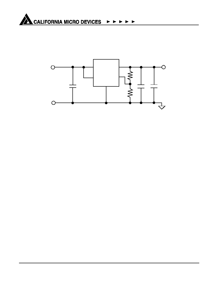
Application Information
Figure 1. Application Circuit for Adjustable Output Operation.
Output Voltage = 1.20 (R1+R2) / R2 [VOLTS]
IN
EN
OUT
GND
10
µ
F
100
n
F
V
OUT
GND
CM3003-XX
ADJ
V
IN
3.3V
10
µ
F
1.5A
R2
R1
© 2004 California Micro Devices Corp. All rights reserved.
6
430 N. McCarthy Blvd., Milpitas, CA 95035-5112
L Tel: 408.263.3214 L Fax: 408.263.7846 L www.calmicro.com
01/15/04
CM3003
Performance Information
CM3003 Typical DC Characteristics (T
A
=25∞C, EN=V
IN
=3.3V, C
IN
=C
OUT
=10uF, unless specified otherwise)
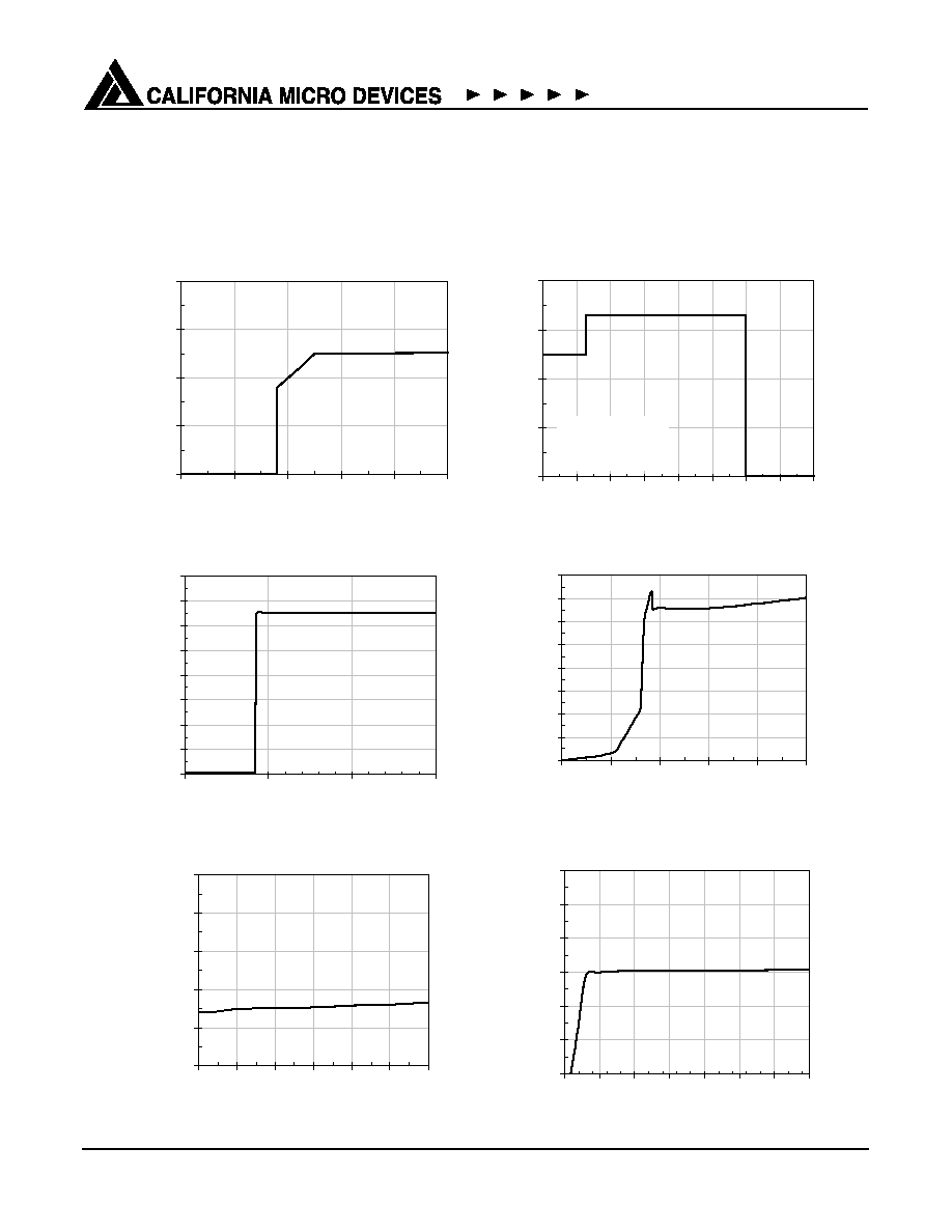
CM3003-25 Device Specfic Data
Output Voltage (10mA Load) with Supply
0.0
1.0
2.0
3.0
4.0
0.0
1.0
2.0
3.0
4.0
5.0
SUPPLY VOLTAGE [V]
OUTPUT VOLTAGE [
V]
Output versus Adjust pin (2.5V)
0
1
2
3
4
0.0
0.2
0.4
0.6
0.8
1.0
1.2
1.4
1.6
ADJUST PIN VOLTAGE [V]
OUTPUT VOLTAGE [
V]
VIN=EN=3.3V
Feedback open
Ground Current with Enable Voltage
0
50
100
150
200
250
300
350
400
0
1
2
3
ENABLE VOLTAGE [V]
GROUND CURRENT [u
A]
Ground Current with Supply (EN = VIN)
0
50
100
150
200
250
300
350
400
0
1
2
3
4
5
SUPPLY VOLTAGE [V]
GROUND CURRENT [u
A]
Ground Current with Output Load
300
320
340
360
380
400
0.0
0.5
1.0
1.5
2.0
2.5
3.0
LOAD CURRENT [Amps]
GROUND CURRENT [u
A]
Internal Reference Voltage with Supply
1.17
1.18
1.19
1.20
1.21
1.22
1.23
1.5
2.0
2.5
3.0
3.5
4.0
4.5
5.0
SUPPLY VOLTAGE [V]
REFERENCE VOLTAGE [
v]
© 2004 California Micro Devices Corp. All rights reserved.
01/15/04
430 N. McCarthy Blvd., Milpitas, CA 95035-5112
L Tel: 408.263.3214 L Fax: 408.263.7846 L www.calmicro.com
7
CM3003
Performance Information (cont'd)
CM3003 Typical DC Characteristics (T
A
=25∞C, EN=V
IN
=3.3V, C
IN
=C
OUT
=10uF, unless specified otherwise)
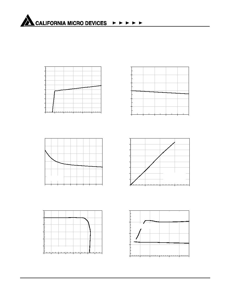
CM3003-25 Device Specfic Data
Line Regulation (2.5V, 10mA Load)
2.40
2.42
2.44
2.46
2.48
2.50
2.52
2.54
2.56
2.58
2.60
2.0
2.5
3.0
3.5
4.0
4.5
5.0
SUPPLY VOLTAGE [V]
OUTPUT VOLTAGE [
V]
Load Regulation
2.47
2.48
2.49
2.50
2.51
2.52
2.53
0.0
0.5
1.0
1.5
2.0
2.5
LOAD CURRENT [Amps]
OUTPUT VOLTAGE [
V]
Dropout Voltage (0.5A) with Supply
0
50
100
150
200
250
300
2.2 2.4 2.6 2.8 3.0 3.2 3.4 3.6 3.8 4.0
SUPPLY VOLTAGE [V]
DROPOUT VOLTAGE [m
V]
0.5A Load
Dropout Voltage with Load
0
50
100
150
200
250
300
350
400
0.0
0.5
1.0
1.5
2.0
LOAD CURRENT [Amps]
DROPOUT VOLTAGE [m
V]
VIN=3.3V
(Adjust Mode)
Current limit protection
2.0
2.1
2.2
2.3
2.4
2.5
2.6
0.0
0.5
1.0
1.5
2.0
2.5
3.0
3.5
4.0
OUTPUT CURRENT [A]
OUTPUT VOLTAGE [
V]
Vdd = 3.3V
Current limit with input voltage
0.0
1.0
2.0
3.0
4.0
2.5
3.0
3.5
4.0
4.5
5.0
5.5
SUPPLY VOLTAGE [V]
OVERLOAD CURRENTS [
A]
DROPOUT
ADJ = 0V
Vout=2.4V
Vout=0.1V
(Short Circuit)
© 2004 California Micro Devices Corp. All rights reserved.
8
430 N. McCarthy Blvd., Milpitas, CA 95035-5112
L Tel: 408.263.3214 L Fax: 408.263.7846 L www.calmicro.com
01/15/04
CM3003
Performance Information (cont'd)
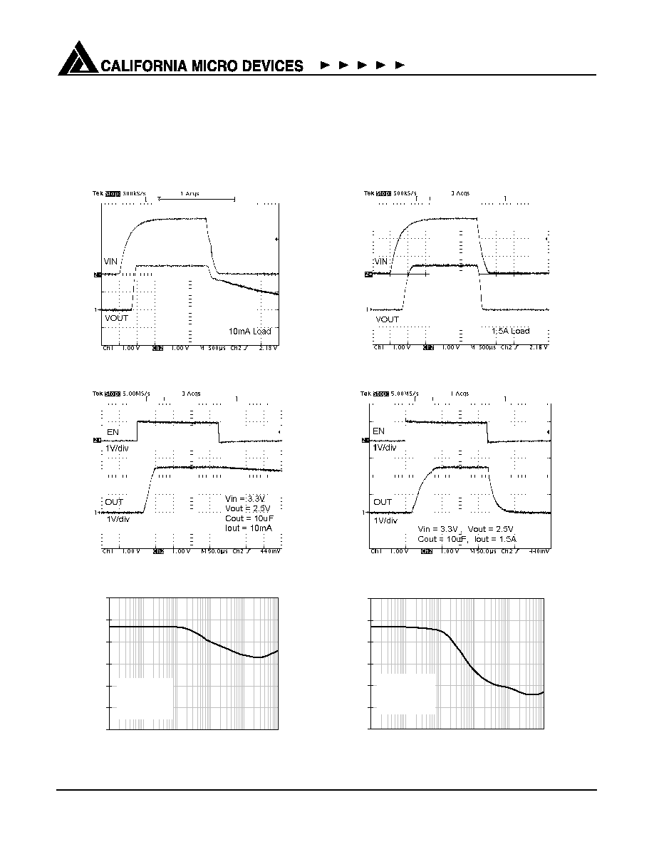
CM3003 Transient Characteristics (T
A
=25∞C, EN=V
IN
=3.3V, C
IN
=C
OUT
=10uF, unless specified otherwise)
CM3003-25 Device Specific Data
Cold Start Power-Up/Down with 10mA Load
Cold Start Power-Up/Down with 1.5A Load
Enable Power-Up with 10mA Load
Enable Power-Up with 1.5A Load
Power Supply Rejection with 25mA Load
0
10
20
30
40
50
60
10
100
1000
10000
100000 1000000
FREQUENCY [Hz]
SUPPLY REJECTION [dB
]
VOUT=2.5V
25mA Load
COUT=10uF
Power Supply Rejection with 1.5A Load
0
10
20
30
40
50
60
10
100
1000
10000
100000 1000000
FREQUENCY [Hz]
SUPPLY REJECTION [dB
]
VOUT=2.5V
1.5A Load
COUT=10uF
© 2004 California Micro Devices Corp. All rights reserved.
01/15/04
430 N. McCarthy Blvd., Milpitas, CA 95035-5112
L Tel: 408.263.3214 L Fax: 408.263.7846 L www.calmicro.com
9
CM3003
Performance Information (cont'd)
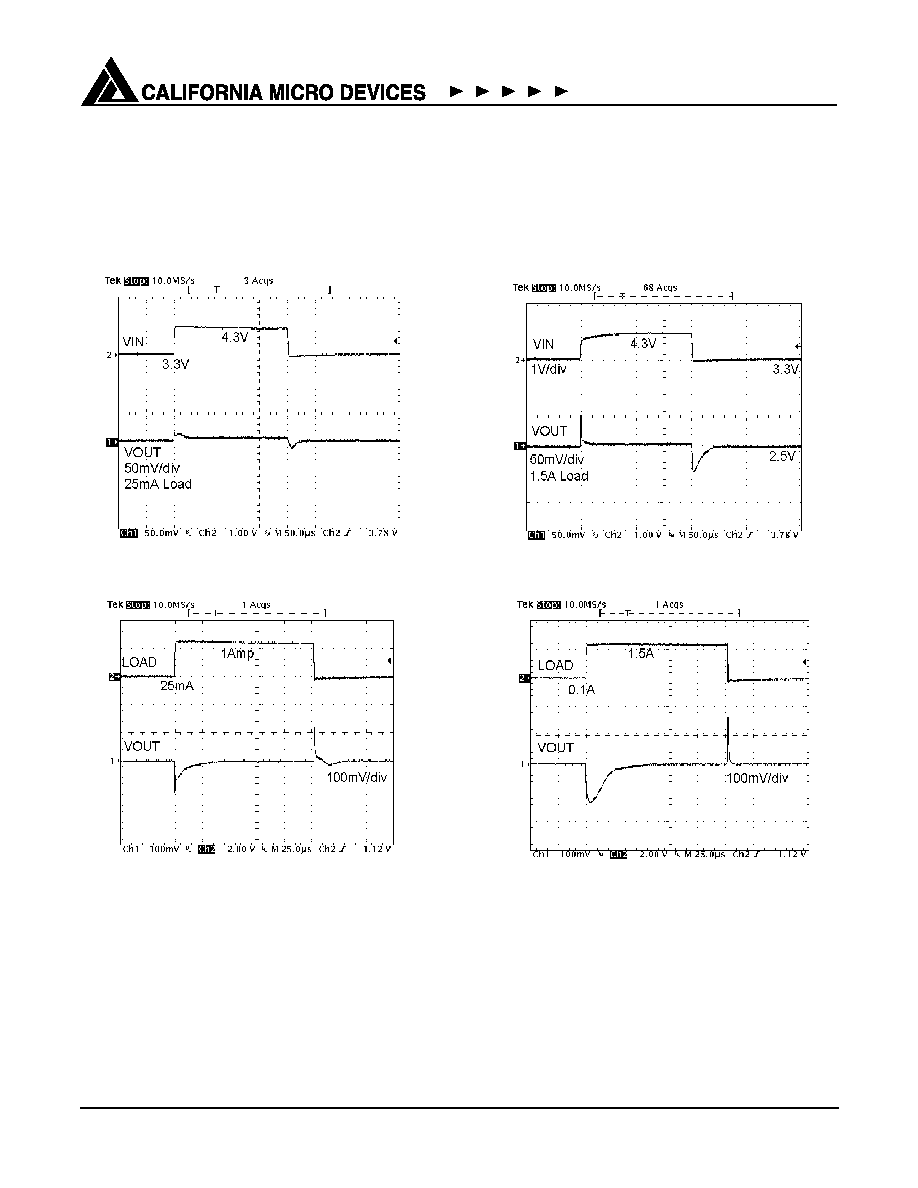
CM3003 Transient Characteristics (T
A
=25∞C, EN=V
IN
=3.3V, C
IN
=C
OUT
=10uF, unless specified otherwise)
CM3003-25 Device Specific Data
Line Transient Response with 25mA Load
Line Transient Response with 1.5A Load
Load Transient Response (25mA to 1A)
Load Transient Response (100mA to 1.5A)
© 2004 California Micro Devices Corp. All rights reserved.
10
430 N. McCarthy Blvd., Milpitas, CA 95035-5112
L Tel: 408.263.3214 L Fax: 408.263.7846 L www.calmicro.com
01/15/04
CM3003
Performance Information (cont'd)
CM3003 Typical Thermal Characteristics
The overall junction to ambient thermal resistance
(
JA
) for device power dissipation (PD) consists prima-
rily of two paths in series. The first path is the junction
to the case (
JC
) which is defined by the package style,
and the second path is case to ambient (
CA
) thermal
resistance which is dependent on board layout. The
final operating junction temperature for any set of con-
ditions can be estimated by the following thermal equa-
tion:
T
JUNC
= T
AMB
+ P
D
(
JC
) + P
D
(
CA
)
= T
AMB
+ P
D
(
JA
)
The CM3003 uses a thermally enhanced package
where all the GND pins (5 through 8) are integral to the
leadframe. When this package is mounted on a double
sided printed circuit board with two square inches of
copper allocated for "heat spreading", the resulting
JA
is about 50∞C/W.
Based on a typical operating power dissipation of 1.0W
(3.0V-2.5Vx 2.0A) with an ambient of 70∞C, the result-
ing junction temperature will be:
T
JUNC
= T
AMB
+ P
D
(
JA
)
= 70∞C + 1.0W X (50∞C/W)
= 70∞C + 50∞C = 120∞C
Thermal characteristics were measured using a double
sided board with two square inches of copper area
connected to the GND pin for "heat spreading".
Measurements showing performance up to junction
temperature of 125∞C were performed under light load
conditions (5mA). This allows the ambient temperature
to be representative of the internal junction tempera-
ture.
Note: The use of multi-layer board construction with
separate ground and power planes will further enhance
the overall thermal performance. In the event of no
copper area being dedicated for heat spreading, a
multi-layer board construction, using only the minimum
size pad layout, will provide the CM3003 with an overall
JA
of 70∞C/W which allows up to 800mW to be safely
dissipated for the maximum junction temperature.
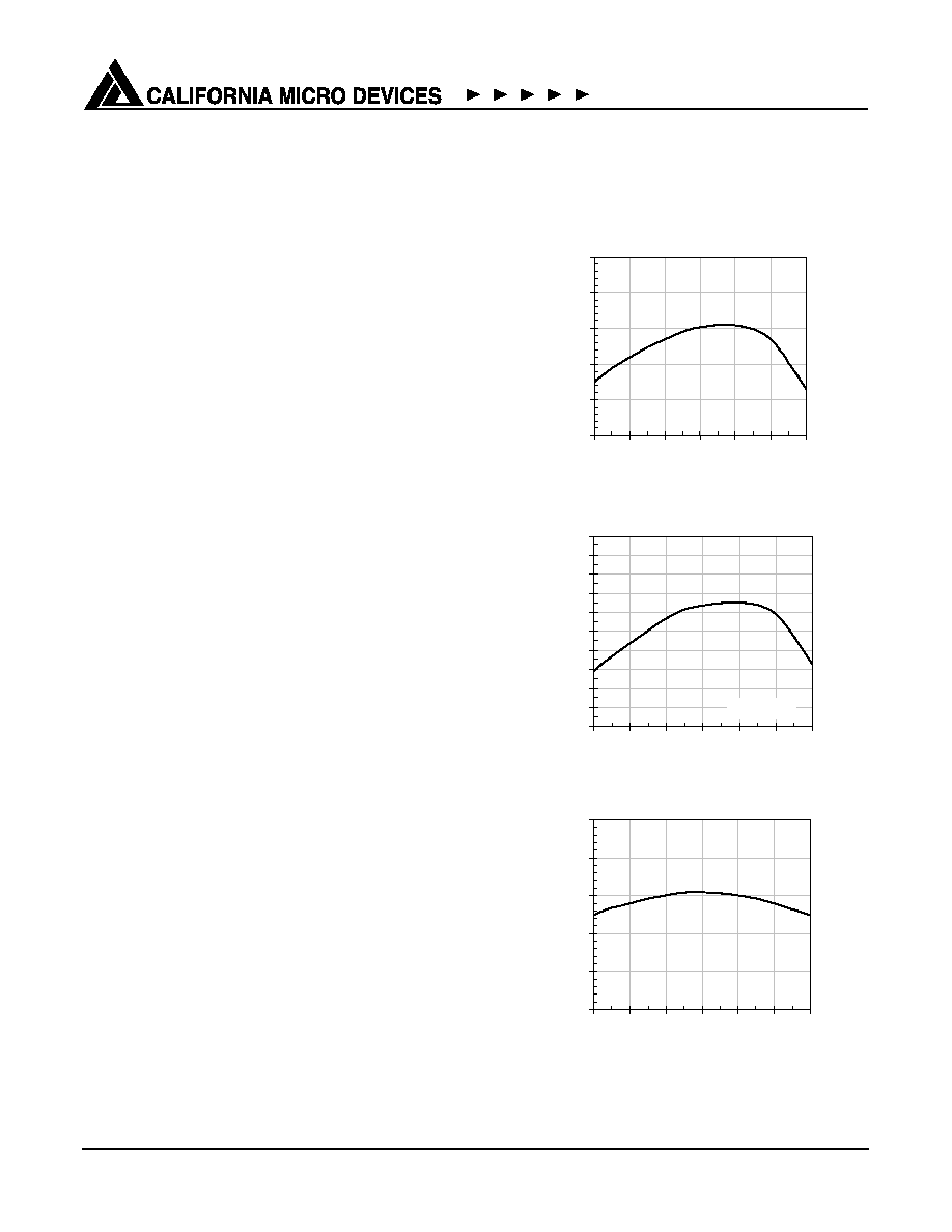
Internal Reference Voltage over Temperature
1.17
1.18
1.19
1.20
1.21
1.22
0
25
50
75
100
125
150
TEMPERATURE [
o
C]
REFERENCE VOLTAGE [
v]
Output Voltage (2.5V) over Temperature
2.45
2.46
2.47
2.48
2.49
2.50
2.51
2.52
2.53
2.54
2.55
0
25
50
75
100
125
150
TEMPERATURE [
o
C]
OUTPUT VOLTAGE [
v]
5mA Load
Ground Current over Temperature
300
310
320
330
340
350
0
25
50
75
100
125
150
TEMPERATURE [
o
C]
GROUND CURRENT [u
A]
© 2004 California Micro Devices Corp. All rights reserved.
01/15/04
430 N. McCarthy Blvd., Milpitas, CA 95035-5112
L Tel: 408.263.3214 L Fax: 408.263.7846 L www.calmicro.com
11
CM3003
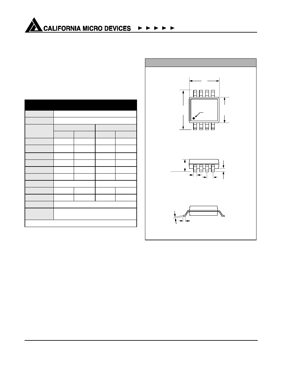
Mechanical Details
SOIC-8 Mechanical Specifications
Dimensions for CM3003 devices packaged in 8-pin
SOIC packages are presented below.
For complete information on the SOIC-8 package, see
the California Micro Devices SOIC Package Informa-
tion document.
* This is an approximate number which may vary.
Package Dimensions for SOIC-8
PACKAGE DIMENSIONS
Package
SOIC
Pins
8
Dimensions
Millimeters
Inches
Min
Max
Min
Max
A
1.35
1.75
0.053
0.069
A
1
0.10
0.25
0.004
0.010
B
0.33
0.51
0.013
0.020
C
0.19
0.25
0.007
0.010
D
4.80
5.00
0.189
0.197
E
3.80
4.19
0.150
0.165
e
1.27 BSC
0.050 BSC
H
5.80
6.20
0.228
0.244
L
0.40
1.27
0.016
0.050
# per tube
100 pieces*
# per tape
and reel
2500 pieces
Controlling dimension: inches
Mechanical Package Diagrams
E
D
H
TOP VIEW
L
END VIEW
C
e
B
A
A
1
SEATING
PLANE
SIDE VIEW
1
2
3
4
8
7
6
5
Pin 1
Marking