
©
2004 California Micro Devices Corp. All rights reserved.
09/14/04
430 N. McCarthy Blvd., Milpitas, CA 95035-5112
Tel: 408.263.3214
Fax: 408.263.7846
www.calmicro.com
1
CM3015
PRELIMINARY
Micropower, 300mA Low Dropout CMOS Regulator
Features
∑
300mA output current capability
∑300mA peak in SOT-23 package
∑300mA continuous in MSOP package
∑
300mV maximum dropout voltage at full load
∑
Excellent line and load regulation
∑
Stable with any output capacitor
∑
Ultra low noise with optional bypass capacitor
∑
Fast power-up with bypass capacitor
∑
"Zero" current in Shutdown mode
∑
Thermal overload protection
∑
Foldback current limiting protection
∑
Reverse current protection
Applications
∑
Notebook and palmtop computers
∑
Cell phones and battery powered devices
∑
Consumer and personal electronics
∑
PC Card V
CC
and V
PP
regulation and switching
CM3015 Regulator Family
* For other output voltages, please consult factory.
Product Description
The CM3015 is a CMOS linear voltage regulator with
low quiescent current, very low dropout voltage and
better than 1% fixed output voltage accuracy. The
CM3015 ground current is typically 150µA at light loads
and only 165µA at 300mA.
Load regulation of 0.25% is maintained for peak cur-
rents up to 300mA. This is useful for supplying in-rush
currents during power-up and transient conditions. The
continuous output current is determined by power dis-
sipation, package type and board layout.
A dedicated control input (EN, Active High) has been
included for power-up sequencing flexibility. When this
input is taken low, the regulator is disabled and the
supply current will drop to near zero.
The CM3015 also features reverse current protection.
This protects the device by blocking the pass transis-
tor's parasitic diode when the output voltage is forced
higher than the input. The device also incorporates
overload current limiting and high temperature thermal
shutdown protection.
For low noise performance and increased power sup-
ply ripple rejection, a bypass capacitor can be con-
nected to the BYP pin. Connecting this capacitor will
not significantly delay the speed of power-up.
To reduce board cost and layout size the CM3015 was
designed to be stable with or without any output capac-
itor. This includes tiny, low ESR ceramic capacitors.
The CM3015 is available in a low profile, 8-lead MSOP
package and 5 and 6-lead SOT23 packages making it
ideal for space critical applications.
PRODUCT
OUTPUT VOLTAGE*
CM3015-00
Adjustable
CM3015-12
1.2V
CM3015-15
1.5V
CM3015-18
1.8V
CM3015-25
2.5V
CM3015-28
2.8V
CM3015-30
3.0V
CM3015-33
3.3V
Block Diagram
EN
+
IN
GND
OUT
-
BYP
V
REF
AMP
EN
Current
Limit
Reverse
Current
Protection
Fast
Power-Up
Enable
Control
Thermal
Overload
Active
Pulldown
R
1
R
2
VSENSE*
* Adjustable output version only

©
2004 California Micro Devices Corp. All rights reserved.
2
430 N. McCarthy Blvd., Milpitas, CA 95035-5112
Tel: 408.263.3214
Fax: 408.263.7846
www.calmicro.com
09/14/04
CM3015
PRELIMINARY
Note 1: Tantalum, electrolytic or low cost ceramic capacitors may be used.
PIN DESCRIPTIONS
SOT23-5
PIN(S)
SOT23-6
PIN(S)
MSOP-8
PIN(S)
NAME
DESCRIPTION
1
1
2
V
IN
V
IN
is the input power source for the regulator. If this input is within a few
inches of the main supply filter, a capacitor may not be necessary. Other-
wise, an input filter capacitor of about 1-10
µF will ensure adequate filter-
ing.
2
2
5-8
GND
The negative reference for all voltages.
3
3
1
EN
Enable input. When this input is taken low (< 0.4V), the regulator is dis-
abled. In this state, the supply current will drop to near zero.
4
4
4
BYP
Reference Bypass Pin. Connect to an external capacitor for noise reduc-
tion. A 10nF-100nF size ceramic capacitor is recommended.
-
5
4
VSENSE
This pin sets V
OUT
with an external divider: V
OUT
= VSENSE(1+ R
1
/R
2
).
R1 is the upper resistor, like the internal divider shown on the block dia-
gram on page 1.
5
6
3
V
OUT
V
OUT
is the output voltage used to power the load. An output capacitor
may not be required for stability, but its use can improve transient
response, noise performance and power supply ripple rejection for fre-
quencies over ~100kHz (see note 1).
V
IN
GND
EN
V
OUT
SENSE
BYP
1
2
6
5
3
4
CC00
TOP VIEW
PACKAGE / PINOUT DIAGRAM
(Note 1)
Notes:
V
IN
GND
EN
V
OUT
BYP
1
2
5
3
4
CC
nn
2
TOP VIEW
1
2
3
4
8
7
6
5
EN
VIN
VOUT
BYP
GND
GND
GND
GND
TOP VIEW
5-PIN SOT23
CM3015-12ST,-15ST,
-18ST,-25ST,-30ST,-33ST
6-PIN SOT23
CM3015-00ST
8-PIN MSOP
CM3015-12MA,-15MA,
-18MA,-25MA,-30MA,-33MA
8-PIN MSOP
CM3015-00MA
1
2
3
4
8
7
6
5
EN
VIN
VOUT
VSENSE
GND
GND
GND
GND
TOP VIEW
CM30
15
n
n
2
CM3
0
1500
2) See Ordering Information section for part marking details.
1) These drawings are not to scale.
©
2004 California Micro Devices Corp. All rights reserved.
09/14/04
430 N. McCarthy Blvd., Milpitas, CA 95035-5112
Tel: 408.263.3214
Fax: 408.263.7846
www.calmicro.com
3
CM3015
PRELIMINARY
Ordering Information
Note 1: Parts are shipped in Tape & Reel form unless otherwise specified.
Specifications
Note 1: Tantalum, electrolytic or low cost ceramic capacitors may be used.
Note 2: V
OUT
+ 1V < V
IN
& 2.5V < V
IN
< 6V, I
OUT
= 1mA, C
IN
= 2.2µF, T
J
= 25
∞
C, C
OUT
= 2.2µF, V
SD
= 1.5V, unless specified other-
wise. Bold values indicate -40
∞
C < T
J
< 125
∞
C
PART NUMBERING INFORMATION
Pins
Package
Ordering Part Number
1
Part Marking
6
SOT23-6
CM3015-00ST
CC00
5
SOT23-5
CM3015-12ST
CC12
5
SOT23-5
CM3015-15ST
CC15
5
SOT23-5
CM3015-18ST
CC18
5
SOT23-5
CM3015-25ST
CC25
5
SOT23-5
CM3015-28ST
CC28
5
SOT23-5
CM3015-30ST
CC30
5
SOT23-5
CM3015-33ST
CC33
8
MSOP-8
CM3015-00MA
CM301500
8
MSOP-8
CM3015-12MA
CM301512
8
MSOP-8
CM3015-15MA
CM301515
8
MSOP-8
CM3015-18MA
CM301518
8
MSOP-8
CM3015-25MA
CM301525
8
MSOP-8
CM3015-28MA
CM301528
8
MSOP-8
CM3015-30MA
CM301530
8
MSOP-8
CM3015-33MA
CM301533
ABSOLUTE MAXIMUM RATINGS
PARAMETER
RATING
UNITS
ESD Protection (HBM)
+2000
V
Pin Voltages
V
IN
EN
V
OUT
[GND - 0.6] to [+6.0]
[GND - 0.6] to [V
CC
+ 0.6]
[GND - 0.6] to [V
CC
+ 0.6]
V
V
V
Storage Temperature Range
-40 to +150
∞C
Operating Temperature Range, Junction
0 to +150
∞C
Power Dissipation (Notes 1,2)
Internally Limited
W
STANDARD OPERATING CONDITIONS
PARAMETER
RATING
UNITS
V
IN
2.2 to 6.0
V
Ambient Operating Temperature Range
-40 to +85
∞C
Load Current
0 to 300
mA
C
EXT
(notes 1 and 2)
0 to 50
µ
F
©
2004 California Micro Devices Corp. All rights reserved.
4
430 N. McCarthy Blvd., Milpitas, CA 95035-5112
Tel: 408.263.3214
Fax: 408.263.7846
www.calmicro.com
09/14/04
CM3015
PRELIMINARY
Specifications (cont'd)
Note 1: V
OUT
+ 1V < V
IN
& 2.5V < V
IN
< 6V, I
OUT
= 1mA, C
IN
= 2.2µF, T
J
= 25
∞
C, C
OUT
= 2.2µF, V
SD
= 1.5V, unless specified other-
wise. Bold values indicate -40
∞
C < T
J
< 125
∞
C
Note 2: Regulation voltages and dropout resistance measured at constant junction temperature using low duty cycle pulse testing.
Note 3: Line regulation is displayed as the average regulation across the full operating range measured in %/V.
ELECTRICAL OPERATING CHARACTERISTICS
(SEE NOTE 1)
SYMBOL PARAMETER
CONDITIONS
MIN
TYP
MAX
UNIT
S
V
OUT
Regulator Output Voltage
T
A
= 25∞C
0∞C<T
J
<125∞C
-40∞C<T
J
<125∞C
-1
-2
-3
+1
+2
+3
%
%
%
V
R LINE
Line Regulation
VOUT + 1V < VIN & 2.5V < VIN < 6V
0.1
0.2
0.4
%/V
V
R LOAD
Load Regulation
0mA
I
OUT
150mA; V
IN
= V
OUT
+ 1V;
Note 2
0.1
0.25
0.50
%
V
SENSE
Reference Voltage
T
A
= 25∞C
1.20
V
R
DROP
Dropout Resistance
1mA
I
LOAD
300mA;
V
IN
= V
OUT
(nominal) -100mV
0.7
1.0
1.2
I
GND
Ground Current
with EN tied to V
IN
; I
LOAD
= 1mA
150
200
µ
A
with EN tied to V
IN
; I
LOAD
= 350mA
165
250
µ
A
with EN tied to GND (Disable Mode)
0.01
1
µ
A
V
EN
Enable Voltage
Regulator enabled
1.5
V
V
DIS
Disable Voltage
Regulator shutdown
0.40
0.18
V
I
EN
Enable Input Current
0.01
µA
PSSR
Power Supply Ripple Rejection
f=1kHz
75
dB
E
NOISE
Output Noise Voltage
10Hz-100kHz; C
BYP
= 0.1
µF
30
µVrms
t
ON
V
OUT
Turn-on Time
C
BYP
= 0
µF
80
µs
C
BYP
= 0.1
µF
100
µs
I
LIM
Overload Current Limit
800
mA
I
SC
Short Circuit Current Limit
V
OUT
< 0.5V
550
mA
T
JSD
Thermal Shutdown Junction
Temperature
165
∞C
T
HYST
Thermal Hysteresis
20
∞C
THERMAL PERFORMANCE
PACKAGE
JA
MINIMUM FOOTPRINT
JA
1" SQUARE 2OZ. COPPER
SOT23-5 / SOT23-6
220∞C/W
170∞C/W
MSOP-8 Fused
160∞C/W
70∞C/W

©
2004 California Micro Devices Corp. All rights reserved.
09/14/04
430 N. McCarthy Blvd., Milpitas, CA 95035-5112
Tel: 408.263.3214
Fax: 408.263.7846
www.calmicro.com
5
CM3015
PRELIMINARY
Performance Information
Typical DC Characteristics (nominal conditions unless specified otherwise)
Nominal Conditions: C
IN
= 1µF, C
OUT
= 2.2µF, No C
BYP
, V
IN
= 4.0V, Load = 5mA (all plots measured with 3.0V
V
OUT
)
Figure 1. Load Regulation
Figure 2. Dropout Voltage (V
OUT
=2.9V)
Figure 3. Foldback Current Limiting
Figure 4. Line Regulation (I
LOAD
=300mA)
Figure 5. Line Regulation (I
LOAD
=5mA)
Figure 6. Line Regulation (I
LOAD
=1mA)
g
2.90
2.95
3.00
3.05
3.10
0
100
200
300
400
500
CURRENT LOAD [mA]
O
U
T
P
U
T
VO
L
T
AG
E
[
V]
0
0.1
0.2
0.3
0.4
0.5
0.6
0.7
0.8
0
100
200
300
400
500
LOAD [mA]
D
R
O
PO
U
T
VO
L
T
AG
E
[
V]
0.0
1.0
2.0
3.0
4.0
0 100 200 300 400 500 600 700 800 900
LOAD CURRENT [mA]
O
U
T
P
U
T
VO
L
T
AG
E
[
V]
2.86
2.88
2.90
2.92
2.94
2.96
2.98
3.00
3
3.5
4
4.5
5
5.5
6
INPUT VOLTAGE [V]
O
U
T
P
U
T
VO
L
T
AG
E
[
V]
2.9
2.92
2.94
2.96
2.98
3
3.02
3.04
3
3.5
4
4.5
5
5.5
6
INPUT VOLTAGE [V]
O
U
T
P
U
T
VO
L
T
AG
E
[
V]
0.0
0.5
1.0
1.5
2.0
2.5
3.0
3.5
4.0
0
1
2
3
4
5
6
INPUT VOLTAGE [V]
O
U
T
P
U
T
VO
L
T
AG
E
[
V]
1mA Load

©
2004 California Micro Devices Corp. All rights reserved.
6
430 N. McCarthy Blvd., Milpitas, CA 95035-5112
Tel: 408.263.3214
Fax: 408.263.7846
www.calmicro.com
09/14/04
CM3015
PRELIMINARY
Performance Information (cont'd)
Typical DC Characteristics (cont'd - nominal conditions unless specified otherwise)
Nominal Conditions: C
IN
= 1µF, C
OUT
= 2.2µF, No C
BYP
, V
IN
= 4.0V, Load = 5mA (all plots measured with 3.0V
V
OUT
)
Figure 7. Enable Voltage Threshold
Figure 8. Supply Current vs. Voltage
(EN=V
IN,
I
LOAD
= 5mA)
Figure 9. Output Supply Current vs. Voltage
Figure 10. Input Supply Current vs. Voltage
Figure 11. Input Supply Current vs. Voltage
Figure 12. Output Supply Current vs. Voltage
500
600
700
800
900
1000
2
3
4
5
6
7
SUPPLY VOLTAGE [V]
TH
R
E
S
H
O
L
D
[
m
V
]
0
50
100
150
200
250
300
350
0
1
2
3
4
5
6
INPUT VOLTAGE (V)
Q
U
I
E
S
C
E
N
T
CURRE
NT
[
µ
A]
0
500
1000
1500
2000
2500
0
1
2
3
4
5
6
OUTPUT SUPPLY VOLTAGE [V]
O
U
T
P
U
T
SU
PPL
Y
C
U
R
R
E
N
T
[
n
A]
V
IN
= 0V, EN = 0V
0
500
1000
1500
2000
2500
0
1
2
3
4
5
6
INPUT SUPPLY VOLTAGE [V]
I
N
PU
T
S
U
PPL
Y
C
U
R
R
E
N
T
[
n
A
]
V
OUT
= 0V, EN = 0V
0
500
1000
1500
2000
2500
0
1
2
3
4
5
6
INPUT SUPPLY VOLTAGE [V]
I
N
PU
T
S
U
PPL
Y
C
U
R
R
EN
T
[
n
A
]
V
OUT
= 3V, EN = 0V
0
1
10
100
1000
10000
0
1
2
3
4
5
6
OUTPUT SUPPLY VOLTAGE [V]
O
U
T
P
UT
S
U
P
P
L
Y
CURRE
NT
[
µ
A]
V
IN
= 3V,
EN = 0V
Clamp to GND
Protect
©
2004 California Micro Devices Corp. All rights reserved.
09/14/04
430 N. McCarthy Blvd., Milpitas, CA 95035-5112
Tel: 408.263.3214
Fax: 408.263.7846
www.calmicro.com
7
CM3015
PRELIMINARY
Performance Information (cont'd)
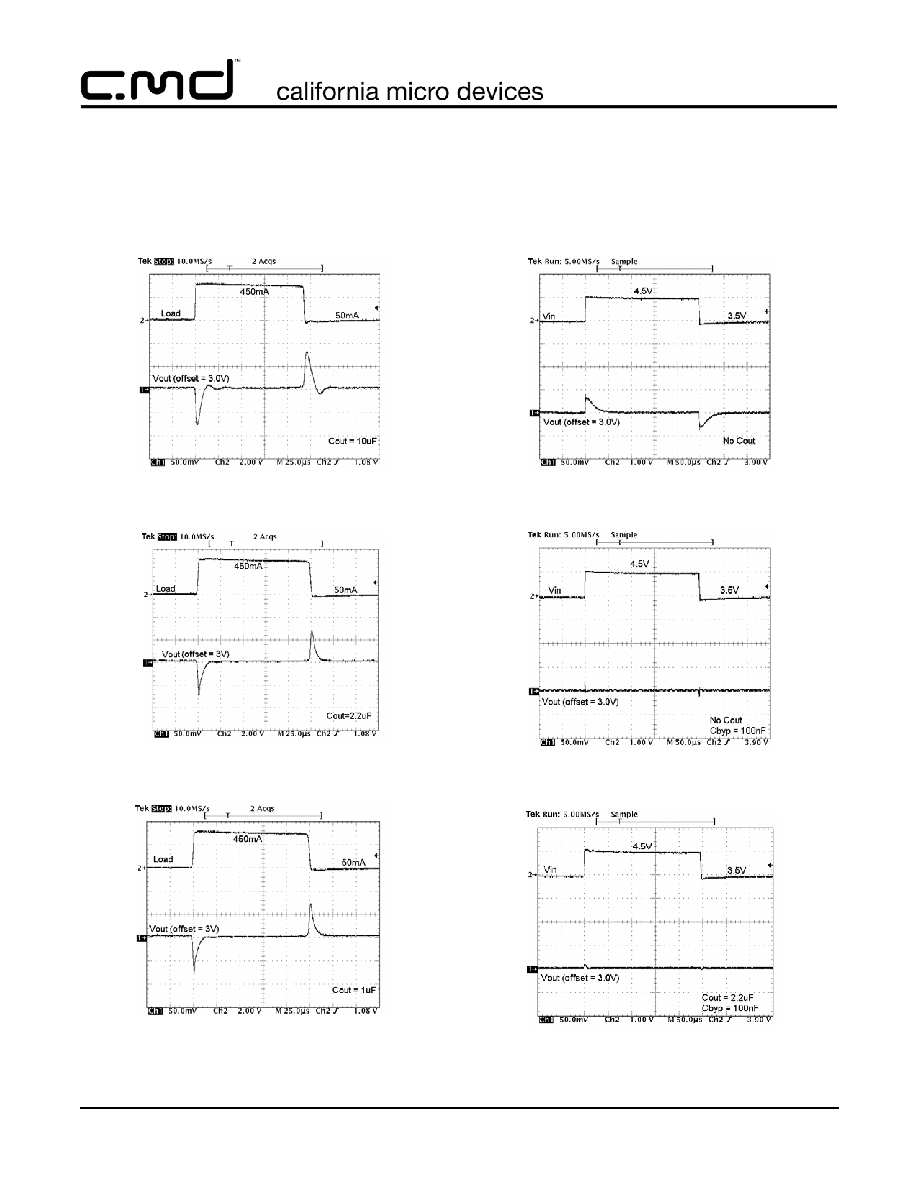
Transient Characteristics (nominal conditions unless specified otherwise)
Nominal Conditions: C
IN
= 1µF, C
OUT
= 2.2µF, No C
BYP
, V
IN
= 4.0V, Load = 5mA
(all plots measured with 3.0V V
OUT
)
Figure 13. 10% to 90% Load Step
(t
r
=1
µs, C
OUT
=10
µF)
Figure 14. 10% to 90% Load Step
(t
r
=1
µs, C
OUT
=2.2
µF)
Figure 15. 10% to 90% Load Step
(t
r
=1
µs, C
OUT
=1.0
µF)
Figure 16. 3.5V - 4.5V Line Step
(t
r
=1
µs, No C
OUT
)
Figure 17. 3.5V - 4.5V Line Step
(t
r
=1
µs, No C
OUT
, C
BYP
=100nF)
Figure 18. 3.5V - 4.5V Line Step
(t
r
=1
µs, C
OUT
=2.2
µF, C
BYP
=100nF)
©
2004 California Micro Devices Corp. All rights reserved.
8
430 N. McCarthy Blvd., Milpitas, CA 95035-5112
Tel: 408.263.3214
Fax: 408.263.7846
www.calmicro.com
09/14/04
CM3015
PRELIMINARY
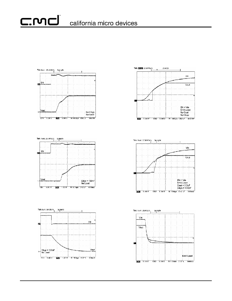
Performance Information (cont'd)
Transient Characteristics (nominal conditions unless specified otherwise)
Nominal Conditions: C
IN
= 1µF, C
OUT
= 2.2µF, No C
BYP
, V
IN
= 4.0V, Load = 5mA
(all plots measured with 3.0V V
OUT
)
Figure 19. Enable Response
(No C
BYP
, No Load)
Figure 20. Enable Response
(C
BYP
=100nF, No Load)
Figure 21. Disable Response
(C
BYP
=100nF, No Load)
Figure 22. Power-Up (EN=V
IN
, I
LOAD
=5mA,
No C
OUT
, No C
BYP
)
Figure 23. Power-Up (EN=V
IN
, I
LOAD
=5mA,
C
OUT
=2.2
µF, C
BYP
=100nF)
Figure 24. Power-Down (I
LOAD
=5mA)

©
2004 California Micro Devices Corp. All rights reserved.
09/14/04
430 N. McCarthy Blvd., Milpitas, CA 95035-5112
Tel: 408.263.3214
Fax: 408.263.7846
www.calmicro.com
9
CM3015
PRELIMINARY
Performance Information (cont'd)
Power Supply Ripple Rejection and Noise Characteristics (nominal conditions unless specified otherwise)
Nominal Conditions: C
IN
= 1µF, V
IN
= 4.0V, PSRR measured with 50mV peak-to-peak sine wave on V
IN
.
Figure 25. Power Supply Ripple Rejection
(C
OUT
=10
µF, C
BYP
=100nF)
Figure 26. Power Supply Ripple Rejection
(C
OUT
=2.2
µF, C
BYP
=100nF)
Figure 27. Power Supply Ripple Rejection
(No C
OUT
, C
BYP
=100nF)
Figure 28. Output Noise Spectral Density
(I
LOAD
=100
µA, C
OUT
=10
µF, C
BYP
=100nF)
Power Supply Ripple Rejection
0
10
20
30
40
50
60
70
80
10
100
1000
10000
100000
Frequency (Hz)
PSRR (dB)
100uA Load
5mA Load
100mA Load
300mA Load
Power Supply Ripple Rejection
0
10
20
30
40
50
60
70
80
10
100
1000
10000
100000
Frequency (Hz)
PSRR (dB)
100uA Load
5mA Load
100mA Load
300mA Load
Power Supply Ripple Rejection
0
10
20
30
40
50
60
70
80
10
100
1000
10000
100000
Frequency (Hz)
PSRR (dB)
100uA Load
5mA Load
100mA Load
300mA Load
Ouput noise spectral density (100uA Load)
1.E-08
1.E-07
1.E-06
1.E+01
1.E+02
1.E+03
1.E+04
1.E+05
Frequency [Hz]
En
[
µ
V
/
r
oot
H
z
]
C
OUT
= 10µF, C
BYP
= 100nF

©
2004 California Micro Devices Corp. All rights reserved.
10
430 N. McCarthy Blvd., Milpitas, CA 95035-5112
Tel: 408.263.3214
Fax: 408.263.7846
www.calmicro.com
09/14/04
CM3015
PRELIMINARY
Performance Information (cont'd)
Typical Thermal Characteristics (nominal conditions unless specified otherwise)
Nominal Conditions: C
IN
= 1µF, C
OUT
= 2.2µF, No C
BYP
, V
IN
= 4.0V, Load = 5mA
(all plots measured with 3.0V V
OUT
)
Figure 29. V
OUT
vs. Temperature
(T
A
= 0
∞
C to 125
∞
C)
Figure 30. V
OUT
vs. Temperature
(T
A
= -40
∞
C to 140
∞
C)
Figure 31. I
GND
vs. Temperature
(T
A
= -40
∞
C to 140
∞
C)
-50
-40
-30
-20
-10
0
10
20
30
40
50
0
25
50
75
100
125
TEMPERATURE [
o
C]
O
U
T
P
U
T
CHA
NG
E
[
m
V
]
-50
-40
-30
-20
-10
0
10
20
30
40
50
-40 -20
0
20 40 60 80 100 120 140
TEMPERATURE [
o
C]
O
U
T
P
U
T
CHA
NG
E
[
m
V
]
0
50
100
150
200
250
300
-40 -20
0
20 40 60 80 100 120 140
TEMPERATURE [
o
C]
G
R
O
UND
CURRE
N
T
[
µ
A]
©
2004 California Micro Devices Corp. All rights reserved.
09/14/04
430 N. McCarthy Blvd., Milpitas, CA 95035-5112
Tel: 408.263.3214
Fax: 408.263.7846
www.calmicro.com
11
CM3015
PRELIMINARY
Application Information
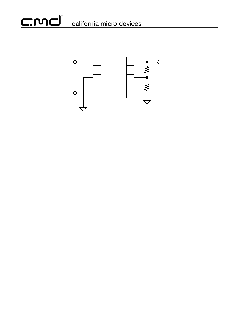
Figure 32. Adjustable Regulator Application Example
Output Compensation
Low-dropout regulator topologies use a current-carry-
ing transistor ("pass device") that adds additional gain
and phase shift to the design. It is necessary to com-
pensate for these attributes to prevent the design from
becoming unstable. The simplest way to do this is to
add an output RC filter to roll off the gain. Since all reg-
ulators use an output capacitor anyway, the only com-
ponent needed is a suitable resistance. Fortunately, for
the usual range and types of output capacitors, this
resistance can be supplied by the ESR of the caps.
For many years, capacitors have been the largest com-
ponents in regulator circuits, but newer types are
shrinking in size rapidly. Unfortunately, their ESRs
have shrunk as well, taking them out of the range
where they can perform the R function described in
existing LDOs. The CM3015 is a new breed of LDO
regulator that can work with these tiny low-ESR capac-
itors and thus permit designs that take a minimum of
space.
An attribute of the LDO topology is that the pass device
gain generally increases with increasing output current.
This may affect output stability: a design that didn't
need a capacitor now does, or a design that used a
small value now needs a larger one. The CMD advan-
tage is that this component can be selected from any
capacitor family without regard to its ESR. If the circuit
calls for a tiny, low-ESR capacitor, it will work just fine.
V
IN
GND
EN
V
OUT
SENSE
BYP
1
2
6
5
3
4
V
IN
=V
OUT
+
R
DROP
(I
OUT
)
V
OUT
=V
SENSE
(1+R1/R2)
V
OUT
=
4.992V
31.6k
10.0k
1.20V
For the input voltage, Vin minimum will depend on the output current. For
example, if Iout is 100mA, Vin must be at least 4.992V = 1ohm x 100mA =
4.992 + 0.1 = 5.092V.
R
1
R
2

©
2004 California Micro Devices Corp. All rights reserved.
12
430 N. McCarthy Blvd., Milpitas, CA 95035-5112
Tel: 408.263.3214
Fax: 408.263.7846
www.calmicro.com
09/14/04
CM3015
PRELIMINARY
Mechanical Details
CM3015 devices are available in a 5-lead SOT23
package, a 6-lead SOT23 package and an 8-lead
MSOP package. Dimensions are presented below and
on the following pages.
SOT23-5 Mechanical Specifications
The dimensions for the 3-lead SOT23 package are
presented below.
Package Dimensions for SOT23-5.
PACKAGE DIMENSIONS
Package
SOT23-5
JEDEC No.
MO-178 (Var. AA)
Pins/Leads
5
Dimensions
Millimeters
Inches
Min
Max
Min
Max
A
--
1.45
--
0.0571
A1
0.00
0.15
0.0000
0.0059
b
0.30
0.50
0.0118
0.0197
c
0.08
0.22
0.0031
0.0087
D
2.75
3.05
0.1083
0.1201
E
2.60
3.00
0.1024
0.1181
E1
1.45
1.75
0.0571
0.0689
e
0.95 BSC
0.0374 BSC
e1
1.90 BSC
0.0748 BSC
L
0.30
0.60
0.0118 0.0236
L1
0.60 REF
0.0236 REF
# per tape
and reel
3000 pieces
Controlling dimension: millimeters
TOP VIEW
e1
e
E1 E
b
5
4
1
2
3
Mechanical Package Diagrams
A
SIDE VIEW
D
A1
L1
END VIEW
c
L

©
2004 California Micro Devices Corp. All rights reserved.
09/14/04
430 N. McCarthy Blvd., Milpitas, CA 95035-5112
Tel: 408.263.3214
Fax: 408.263.7846
www.calmicro.com
13
CM3015
PRELIMINARY
Mechanical Details (cont'd)
SOT23-6 Mechanical Specifications
The dimensions for the 6-lead SOT23 package are
presented below.
Package Dimensions for SOT23-6.
PACKAGE DIMENSIONS
Package
SOT23-6
JEDEC No.
MO-178 (Var. AB)
Pins/Leads
6
Dimensions
Millimeters
Inches
Min
Max
Min
Max
A
--
1.45
--
0.0571
A1
0.00
0.15
0.0000
0.0059
b
0.30
0.50
0.0118
0.0197
c
0.08
0.22
0.0031
0.0087
D
2.75
3.05
0.1083
0.1201
E
2.60
3.00
0.1024
0.1181
E1
1.45
1.75
0.0571
0.0689
e
0.95 BSC
0.0374 BSC
e1
1.90 BSC
0.0748 BSC
L
0.30
0.60
0.0118
0.0236
L1
0.60 REF
0.0236REF
# per tape
and reel
3000 pieces
Controlling dimension: millimeters
TOP VIEW
1
2
3
6
5
4
e1
e
E1 E
b
Pin 1
Marking
Mechanical Package Diagrams
A
SIDE VIEW
D
A1
L1
END VIEW
c
L

©
2004 California Micro Devices Corp. All rights reserved.
14
430 N. McCarthy Blvd., Milpitas, CA 95035-5112
Tel: 408.263.3214
Fax: 408.263.7846
www.calmicro.com
09/14/04
CM3015
PRELIMINARY
Mechanical Details (cont'd)
MSOP-8 Mechanical Specifications:
The dimensions for the 6-lead SOT23 package are
presented below.
* This is an approximate amount which may vary.
Package Dimensions for MSOP-8
PACKAGE DIMENSIONS
Package
MSOP
Pins
8
Dimensions
Millimeters
Inches
Min
Max
Min
Max
A
0.87
1.17
0.034
0.046
A1
0.05
0.25
0.002
0.010
B
0.30 (typ)
0.012 (typ)
C
0.18
0.007
D
2.90
3.10
0.114
0.122
E
2.90
3.10
0.114
0.122
e
0.65 BSC
0.025 BSC
H
4.78
4.98
0.188
0.196
L
0.52
0.54
0.017
0.025
# per tube
80 pieces*
# per tape
and reel
4000 pieces
Controlling dimension: inches
Mechanical Package Diagrams
E
D
H
1
2
3
4
8
7
6
5
L
END VIEW
C
e
B
A
A1
SEATING
PLANE
SIDE VIEW
TOP VIEW
Pin 1
Marking