 | –≠–ª–µ–∫—Ç—Ä–æ–Ω–Ω—ã–π –∫–æ–º–ø–æ–Ω–µ–Ω—Ç: CM3016-48 | –°–∫–∞—á–∞—Ç—å:  PDF PDF  ZIP ZIP |
©
2004 California Micro Devices Corp. All rights reserved.
430 N. McCarthy Blvd., Milpitas, CA 95035-5112
Tel: 408.263.3214
Fax: 408.263.7846
www.calmicro.com
CM3016-48
V2.XX
12/22/04
1
Micropower, 4.75V/500mA Low Noise CMOS LDO Regulator
Features
∑
Linear LDO regulator with 4.75V output
∑
500mA output current capability
- 500mA peak in SOT-23 package
∑
500mV maximum dropout voltage at full load
∑
150mV maximum dropout at 150mA load
∑
Excellent line and load regulation
∑
Stable with low ESR output capacitor
∑
Ultra low noise with optional bypass capacitor
∑
Fast power-up with bypass capacitor
∑
"Zero" current in Shutdown mode
∑
Thermal Overload Protection
∑
Foldback Current Limiting Protection
∑
Reverse current protection
∑
Lead-free version available
Applications
∑
Notebook computers
∑
Consumer and personal electronics
∑
Ideal for powering audio codecs
Product Description
The CM3016-48 is a CMOS linear voltage regulator with
low quiescent current, very low drop out voltage and better
than 1% initial output voltage accuracy. The quiescent cur-
rent is typically 150
µA at light loads and only 165µA at
500mA. This is 5% more efficient than equivalent Bi-CMOS
devices that can waste up to 25mA at 500mA load. The
CM3016-48 can maintain load regulation for peak currents
up to 500mA, which is useful for supplying inrush currents
during power-up and transient conditions. Continuous out-
put current is limited by package type and board layout.
A dedicated control input (EN, Active High) has been
included for power-up sequencing flexibility. When this input
is taken low, the regulator is disabled. In this state, the sup-
ply current will drop to near zero. The device also features
reverse current protection. This protects the device by
blocking the pass transistors parasitic diode when the out-
put voltage is forced higher than the input.
For low noise performance and increased power supply rip-
ple rejection a noise bypass capacitor can be connected to
the BYP pin. Connecting this capacitor will not significantly
delay the speed of power-up.
The CM3016-48 is fully protected, offering both overload
current limiting and high temperature thermal shutdown. To
reduce board cost and layout size, the CM3016 was
designed to be stable with or without an output capacitor.
This includes tiny, low ESR ceramic capacitors.
The CM3016-48 is housed in a 5-pin SOT23 package and
is ideal for space critical applications. It is available with
optional lead-free finishing.
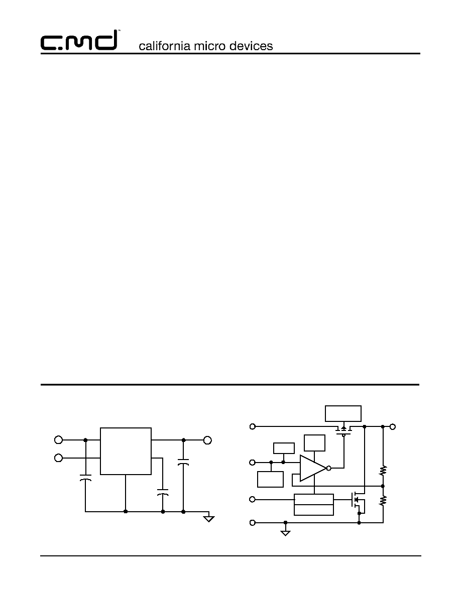
Simplified Electrical Schematic
Typical Application Circuit
EN
+
IN
GND
OUT
-
BYP
V
REF
Enable Control
Thermal Overload
Fast
Power-Up
Current
Limit
EN
AMP
Reverse Current
Protection
IN
EN
OUT
GND
1
µ
F
2.2
µ
F
OUT
+
+
C
OUT
C
IN
CM3016-48
100
n
F
+
C
BYP
BYP
IN
EN
V2.xx
430 N. McCarthy Blvd., Milpitas, CA 95035-5112
Tel: 408.263.3214
Fax: 408.263.7846
www.calmicro.com
CM3016-48
2
12/22/04
Ordering Information
Note 1: Parts are shipped in Tape & Reel form unless otherwise specified.
PACKAGE / PINOUT DIAGRAM
Note: This drawing is not to scale.
5-pin SOT23
IN
GND
EN
1
2
5
3
4
OUT
BYP
Top View
PIN DESCRIPTIONS
SOT23-5
NAME
DESCRIPTION
PIN(S)
1
IN
Regulator input. If this input is within a few inches of the main supply filter, a capacitor may not be
necessary. Otherwise an input filter capacitor of 1-10
µF will ensure adequate filtering.
2
GND
Ground is the negative reference for all voltages
3
EN
Enable input. When this input is taken low (< 0.4V), the regulator is disabled. In this state, the sup-
ply current will drop to near zero.
4
BYP
Reference bypass input. Connect to an external capacitor for noise reduction. A 10nF-100nF
ceramic capacitor is recommended.
5
OUT
Regulator output. No output capacitor is required for stability. Any type of output capacitor can be
added to improve transient response, noise performance and power supply ripple rejection for fre-
quencies over ~100kHz.
PART NUMBERING INFORMATION
Pins
Package
Standard Finish
Lead-free Finish
Ordering Part
Number
1
Part Marking
Ordering Part
Number
1
Part Marking
5
SOT23
CM3016-48ST
CA48
CM3016-48SO
CR48

V2.XX
430 N. McCarthy Blvd., Milpitas, CA 95035-5112
Tel: 408.263.3214
Fax: 408.263.7846
www.calmicro.com
CM3016-48
12/22/04
3
Specifications
Note 1: The CM3016-48 contains a thermal overload circuit that automatically disables the device thereby preventing excessive
junction temperature. When the SOT23-5 package housing the device is mounted on a typical multi-layer board with moder-
ate heat spreading copper area (2 square inches) will allow up to 0.315W to be safely dissipated. Please consult with factory
for thermal evaluation assistance.
Note 2: Consult CAMD Technical Support for power dissipation information regarding the CM3016-48 packaged in the SOT23 pack-
age.
ABSOLUTE MAXIMUM RATINGS
PARAMETER
RATING
UNITS
Pin Voltages
IN
EN
OUT
[GND - 0.6] to [+6.0]
[GND - 0.6] to [V
IN
+ 0.6]
[GND - 0.6] to [V
IN
+ 0.6]
V
V
V
Storage Temperature Range
-40 to +150
∞C
Operating Temperature Range
Ambient
Junction
-40 to +85
0 to +150
∞C
∞C
Power Dissipation (Notes 1,2)
Internally Limited
W
STANDARD OPERATING CONDITIONS
PARAMETER
RATING
UNITS
V
IN
[V
OUT
+ 0.15] to 6.0
VDC
Ambient Operating Temperature Range
-40 to +85
∞C
Load Current
0 to 500
mA
C
OUT
0 -100
µ
F

V2.xx
430 N. McCarthy Blvd., Milpitas, CA 95035-5112
Tel: 408.263.3214
Fax: 408.263.7846
www.calmicro.com
CM3016-48
4
12/22/04
Specifications (continued)
Note 1: V
OUT
+1V< V
IN
& 2.5V< V
IN
< 6V, I
OUT
=1mA, C
IN
=2.2uF, T
J
=25∞C, unless specified otherwise. Bold values
indicate -40∞C < T
J
< 125∞C
Note 2: Tantalum, electrolytic or low ESR ceramic capacitors may be used for C
OUT
.
Note 3: Regulation voltages and dropout resistance is measured at constant junction temperature using low duty
cycle pulse testing.
Note 4: Line regulation is displayed as the average regulation across the full operating range measured in %/V.
ELECTRICAL OPERATING CHARACTERISTICS
(SEE NOTE1)
SYMBOL PARAMETER
CONDITIONS
MIN
TYP
MAX
UNITS
V
OUT
Output Voltage
T
A
= 25∞C
0∞C < T
J
< 125∞C
-40∞C < T
J
< 125∞C
4.70
4.66
4.61
4.75
4.75
4.75
4.80
4.85
4.89
V
V
V
V
R LINE
Line Regulation (see Note 4)
V
OUT
+1V < V
IN
and 2.5V < V
IN
< 6V
0.1
0.2
0.4
%
%
V
R LOAD
Load Regulation
I
OUT
=1mA to 500mA;
V
IN
=V
OUT
+1V; Note 3
0.1
0.5
0.8
%
%
R
DROP
Dropout Resistance
I
OUT
=1mA to 500mA;
V
IN
=V
OUT
(nominal)-100mV
0.7
1
1.2
I
GND
Ground Current
with EN tied to V
IN
; I
LOAD
=1mA:
150
200
µ
A
with EN tied to V
IN
; I
LOAD
=150mA:
165
200
µ
A
with EN tied to GND (Disable Mode):
0.01
1
µ
A
V
EN
Enable Voltage
Regulator becomes enabled
1.5
V
V
DIS
Disable Voltage
Regulator enters shutdown
0.4
0.18
V
V
I
EN
Enable Input Current
0.01
µ
A
E
NOISE
Output Noise Voltage
BW=10Hz-100kHz; C
OUT
= 2.2
µF;
C
BYP
= 0.1
µF
30
µVrms
t
ON
V
OUT
Turn-on Time
C
BYP
= 0
µF; C
OUT
= 2.2
µF
80
µ
S
C
BYP
= 0.1
µF; C
OUT
= 2.2
µF
100
µ
S
I
LIM
Overload Current Limit
800
mA
I
SC
Short Circuit Current Limit
V
OUT
< 0.5V
550
mA
T
JSD
Thermal Shutdown Junction
Temperature
165
∞C
T
HYST
Thermal Hysteresis
20
∞C
THERMAL PERFORMANCE
PACKAGE
JA
MINIMUM FOOTPRINT
JA
1" SQUARE 2OZ. COPPER
SOT23-5
220∞C/W
170∞C/W
V2.XX
430 N. McCarthy Blvd., Milpitas, CA 95035-5112
Tel: 408.263.3214
Fax: 408.263.7846
www.calmicro.com
CM3016-48
12/22/04
5
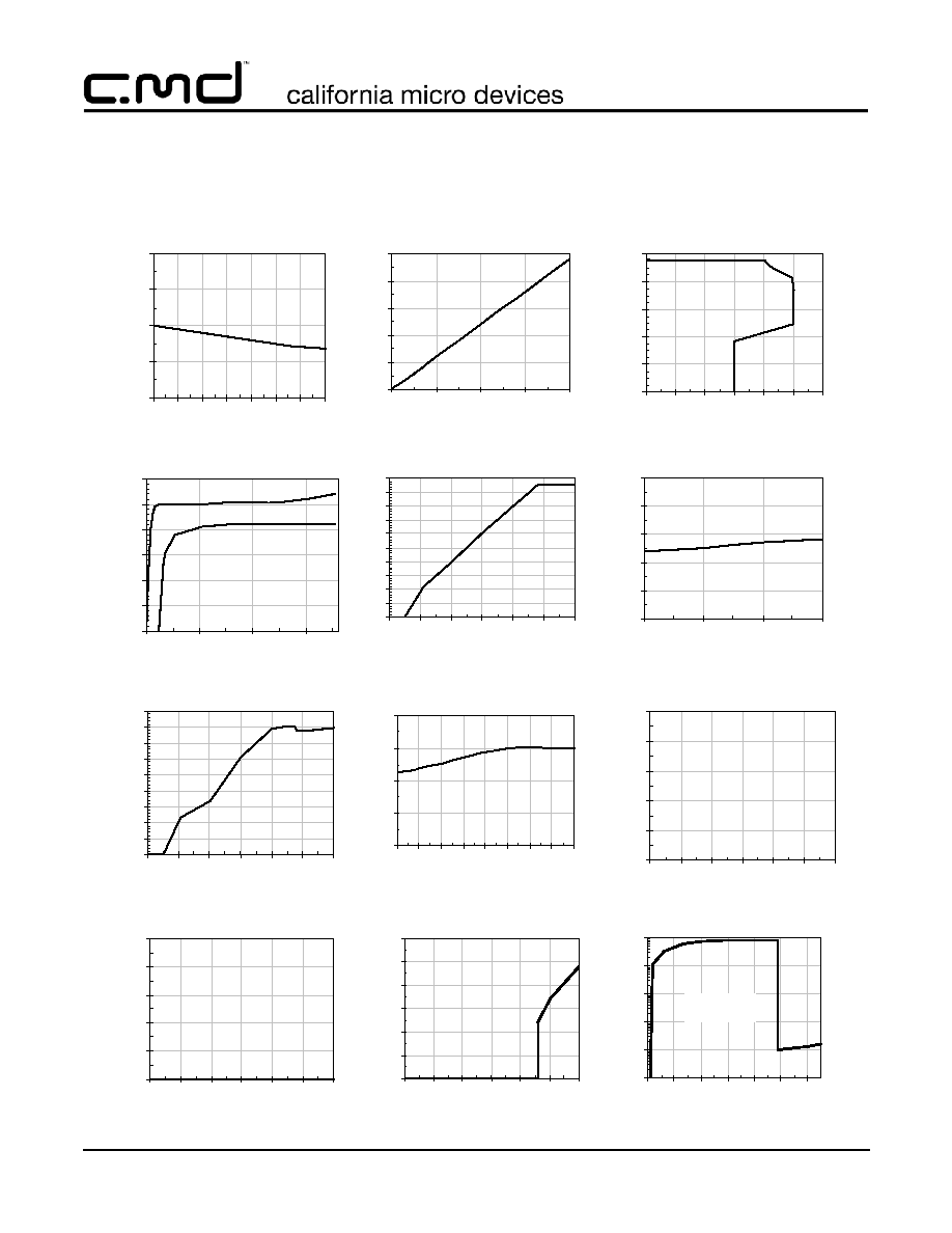
Performance Information
Typical DC Characteristics (nominal conditions unless otherwise specified, CM3016-48ST Only)
C
IN
= 2.2uF, C
OUT
= 2.2uF, No C
BYP
,, V
IN
= 5.75V, Load = 5mA
Load Regulation
4.700
4.725
4.750
4.775
4.800
0
100
200 300 400 500 600
700
LOAD CURRENT [mA]
OUTPUT VOLTAGE [V]
Dropout Voltage (Vout=4.7V)
0
100
200
300
400
500
0
200
400
600
800
LOAD [mA]
DROPOUT [mV]
Foldback Current Limiting
0.0
1.0
2.0
3.0
4.0
5.0
0
200
400
600
800
1000 1200
LOAD CURRENT [mA]
OUTPUT VOLTAGE [V]
Line Regulation
4.70
4.71
4.72
4.73
4.74
4.75
4.76
4.7
5.2
5.7
6.2
INPUT VOLTAGE [V]
OUTPUT VOLTAGE [V]
1mA Load
200mA Load
Line Regulation
0.0
0.5
1.0
1.5
2.0
2.5
3.0
3.5
4.0
4.5
5.0
0
1
2
3
4
5
6
INPUT VOLTAGE [V]
OOUTPUT VOLTAGE [V]
1mA Load
Enable Voltage Threshold
500
600
700
800
900
1000
4.5
5.0
5.5
6.0
SUPPLY VOLTAGE [V]
THRESHOLD [mV]
Supply Current vs. Voltage (EN = VIN)
0
20
40
60
80
100
120
140
160
180
0
1
2
3
4
5
6
INPUT VOLTAGE [V]
GROUND CURRENT [uA]
1mA Load
En = Vin
Ground Current vs. Output Load
100
125
150
175
200
0
100 200 300 400 500 600 700 800
LOAD CURRENT [mA]
GROUND CURRENT [uA]
Output Supply Current vs. Voltage
0
500
1000
1500
2000
2500
0
1
2
3
4
5
6
OUTPUT SUPPLY VOLTAGE [V]
OUTPUT SUPPLY CURRENT [nA]
Vin = 0V, EN = 0V
Input Supply Current vs. Voltage
0
500
1000
1500
2000
2500
0
1
2
3
4
5
6
INPUT SUPPLY VOLTAGE [V]
INPUT SUPPLY CURRENT [nA]
Vout = 0V, EN = 0V
Input Supply Current vs. Voltage
0
500
1000
1500
2000
2500
3000
0
1
2
3
4
5
6
INPUT SUPPLY VOLTAGE [V]
INPUT SUPPLY CURRENT [nA]
Vout = 4.75V, EN = 0V
Output Supply Current vs. Voltage
0
1
10
100
1000
10000
0.0
1.0
2.0
3.0
4.0
5.0
6.0
OUTPUT SUPPLY VOLTAGE [V]
OUTPUT SUPPLY CURRENT [uA
]
Vin = 4.75V,
EN = 0V
Clamp to GND
Protect
V2.xx
430 N. McCarthy Blvd., Milpitas, CA 95035-5112
Tel: 408.263.3214
Fax: 408.263.7846
www.calmicro.com
CM3016-48
6
12/22/04
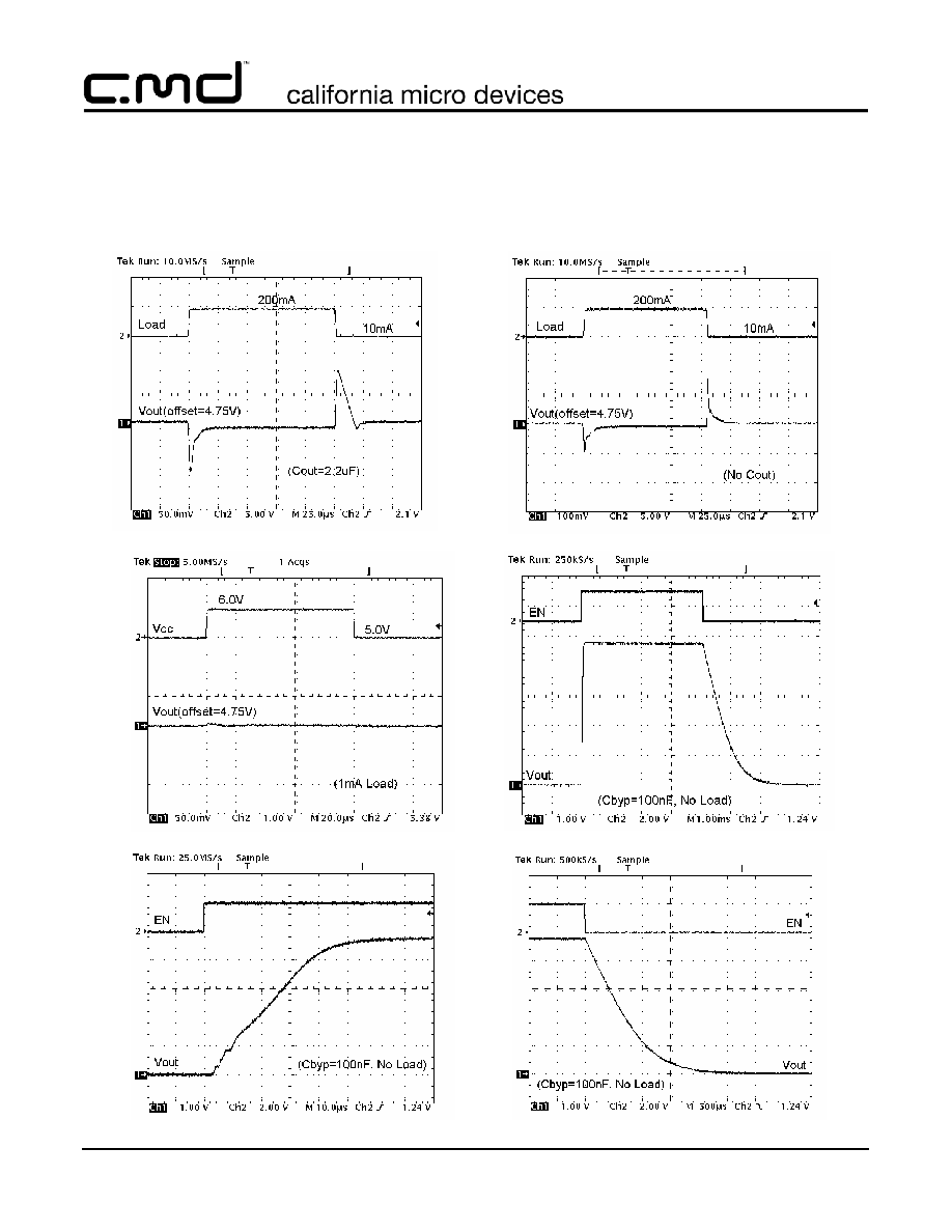
Performance Information (cont'd)
Transient Characteristics (nominal conditions unless otherwise specified, CM3016-48ST Only)
C
IN
= 2.2uF, C
OUT
= 2.2uF, C
BYP
= 0.1uF, V
IN
= 5.0V, Load = 5mA,
Load Step Response
Load Step Response
Line Step Response
Enable, Disable Response
Enable Response
Disable Response
V2.XX
430 N. McCarthy Blvd., Milpitas, CA 95035-5112
Tel: 408.263.3214
Fax: 408.263.7846
www.calmicro.com
CM3016-48
12/22/04
7
Performance Information (cont'd)
Power Supply Ripple Rejection (nominal conditions unless otherwise specified, CM3016-48ST Only)
C
IN
= 1uF, V
IN
= 5.0V, Load = 5mA, PSRR measured with 10mV pk-pk sin wave on V
IN
.
PSRR (VIN-VOUT = 500mV)
0
10
20
30
40
50
60
70
80
10
100
1000
10000
100000
Frequency [Hz]
PSRR [dB]
Cout=2.2uF, Cbyp=100nF, Vin-Vout=500mV
500mA
400mA
300mA
200mA
100mA
50mA
20mA
5mA
0.1mA
PSRR (VIN-VOUT = 250mV)
0
10
20
30
40
50
60
70
80
10
100
1000
10000
100000
Frequency [Hz]
PSRR [dB]
Cout=2.2uF, Cbyp=100nF, Vin-Vout=250mV
400mA
300mA
200mA
100mA
50mA
20mA
5mA
0.1mA
PSRR (VIN-VOUT = 200mV)
0
10
20
30
40
50
60
70
80
10
100
1000
10000
100000
Frequency [Hz]
PSRR [dB]
Cout=2.2uF, Cbyp=100nF, Vin-Vout=200mV
300mA
200mA
100mA
50mA
20mA
5mA
0.1mA
PSRR (VIN-VOUT = 175mV)
0
10
20
30
40
50
60
70
80
1 0
100
1000
10000
100000
Frequency [Hz]
PSRR [dB]
Cout=2.2uF, Cbyp=100nF, Vin-Vout=175mV
200mA
100mA
50mA
20mA
5mA
0.1mA
V2.xx
430 N. McCarthy Blvd., Milpitas, CA 95035-5112
Tel: 408.263.3214
Fax: 408.263.7846
www.calmicro.com
CM3016-48
8
12/22/04
Performance Information (cont'd)
Power Supply Ripple Rejection (nominal conditions unless otherwise specified, CM3016-48ST Only)
C
IN
= 1uF, V
IN
= 5.0V, Load = 5mA, PSRR measured with 10mV pk-pk sin wave on V
IN
.
PSRR (VIN-VOUT = 150mV)
0
10
20
30
40
50
60
70
80
10
100
1000
10000
100000
Frequency [Hz]
PSRR [dB]
Cout=2.2uF, Cbyp=100nF, Vin-Vout=150mV
200mA
100mA
50mA
20mA
5mA
0.1mA
PSRR (VIN-VOUT = 125mV)
0
10
20
30
40
50
60
70
80
10
100
1000
10000
100000
Frequency [Hz]
PSRR [dB]
Cout=2.2uF, Cbyp=100nF, Vin-Vout=125mV
100mA
50mA
20mA
5mA
0.1mA
PSRR (VIN-VOUT = 100mV)
0
10
20
30
40
50
60
70
80
10
100
1000
10000
100000
Frequency [Hz]
PSRR [dB]
Cout=2.2uF, Cbyp=100nF, Vin-Vout=100mV
100mA
50mA
20mA
5mA
0.1mA

V2.XX
430 N. McCarthy Blvd., Milpitas, CA 95035-5112
Tel: 408.263.3214
Fax: 408.263.7846
www.calmicro.com
CM3016-48
12/22/04
9
Performance Information (cont'd)
Typical Thermal Characteristics (nominal conditions unless otherwise specified, CM3016-48ST Only)
C
IN
= 2.2uF, C
OUT
= 2.2uF, No C
BYP ,
V
IN
= 5.0V, Load = 5mA.
VOUT vs. Temperature (200mA Load)
-50
-40
-30
-20
-10
0
10
20
30
40
50
-40 -20
0
20
40
60
80
100 120
TEMPERATURE [
o
C]
OUTPUT CHANGE [mV]
VOUT vs. Temperature
-20
-15
-10
-5
0
5
10
15
20
0
25
50
75
100
125
150
JUNCTION TEMPERATURE [
o
C]
OUTPUT CHANGE [mV]
Ignd vs. Temperature
0
50
100
150
200
250
300
-40 -20
0
20
40 60
80 100 120 140
TEMPERATURE [
o
C]
GROUND CURRENT [uA]
Dropout Resistance vs. Temperature
0.0
0.2
0.4
0.6
0.8
1.0
-40
0
40
80
120
160
TEMPERATURE [
o
C]
Dropout Resistance [Ohms]

V2.xx
430 N. McCarthy Blvd., Milpitas, CA 95035-5112
Tel: 408.263.3214
Fax: 408.263.7846
www.calmicro.com
CM3016-48
10
12/22/04
Mechanical Details
The CM3016-48 is available in a 5-pin SOT23 pack-
age. Dimensions for this package is presented below.
SOT23-5 Mechanical Specifications
Dimensions for CM3016-48ST/SO devices packaged
in a 5-pin SOT23 package are presented below.
For complete information on the SOT23 package, see
the California Micro Devices SOT23 Package Informa-
tion document.
Package Dimensions for SOT23-5.
PACKAGE DIMENSIONS
Package
SOT23 (JEDEC name is MO-178)
Pins
5
Dimensions
Millimeters
Inches
Min
Max
Min
Max
A
--
1.45
--
0.057
A1
0.00
0.15
0.000
0.006
b
0.30
0.50
0.012
0.020
c
0.08
0.22
0.003
0.009
D
2.75
3.05
0.108
0.120
E
2.60
3.00
0.102
0.118
E1
1.45
1.75
0.057
0.069
e
0.95 BSC
0.0374 BSC
e1
1.90 BSC
0.0748 BSC
L
0.60 REF
0.0236 REF
# per tape
and reel
3000 pieces
Controlling dimension: inches
TOP VIEW
5
4
e1
e
E1 E
b
A
SIDE VIEW
L1
END VIEW
D
A1
c
1
2
3
Mechanical Package Diagrams