 | –≠–ª–µ–∫—Ç—Ä–æ–Ω–Ω—ã–π –∫–æ–º–ø–æ–Ω–µ–Ω—Ç: CM3019-18 | –°–∫–∞—á–∞—Ç—å:  PDF PDF  ZIP ZIP |

CALIFORNIA MICRO DEVICES
Preliminary
CM3019
© 2004 California Micro Devices Corp. All rights reserved
02/20/04
430 N. McCarthy Blvd, Milpitas, California 95035 Tel: (408) 263-3214 Fax: (408) 263-7846 www.calmicro.com
1
Micropower, 500mA Low Noise CMOS LDO Regulator
Features
∑ 500mA output current capability
∑ 500mA peak in SOT-23 package
∑ 500mA continuous in MSOP package
∑ 500mV maximum dropout voltage at full load
∑ Excellent line and load regulation
∑ Stable with any output capacitor
∑ Ultra low noise with optional bypass capacitor
∑ Fast power-up with bypass capacitor
∑ "Zero" current in Shutdown mode
∑ Thermal Overload Protection
∑ Foldback Current Limiting Protection
∑ Reverse current protection
Applications
∑ Notebook, and palmtop computers
∑ Cell phones and battery powered devices
∑ Consumer and personal electronics
∑ PC Card Vcc and Vpp regulation and switching
Table 1: CM3019 Regulator Family
Product
Output Voltage
CM3019-00 Adjustable
CM3019-12 1.2V
CM3019-15 1.5V
CM3019-18 1.8V
CM3019-25 2.5V
CM3019-28 2.8V
CM3019-30 3.0V
CM3019-33 3.3V
For other output voltages, please contact the factory
Product Description
The CM3019 is a CMOS linear voltage regulator with low
quiescent current, very low drop out voltage and better
than 1% initial output voltage accuracy.
The quiescent current is typically 150µA at light loads and
only 165µA at 500mA. This is 5% more efficient than
equivalent Bi-CMOS devices that can waste up to 25mA at
500mA.
Load regulation is maintained for peak currents up to
500mA. This is useful for supplying inrush currents during
power-up and transient conditions. Continuous output
current is limited by package type and board layout.
A dedicated control input (EN, Active High) has been
included for power-up sequencing flexibility. When this
input is taken low, the regulator is disabled. In this state,
the supply current will drop to near zero.
The device also features reverse current protection. This
protects the device by blocking the pass transistors
parasitic diode when the output voltage is forced higher
than the input.
For low noise performance and increased power supply
ripple rejection a noise bypass capacitor can be connected
to the BYP pin. Connecting this capacitor will not
significantly delay the speed of power-up.
The CM3019 is fully protected, offering both overload
current limiting and high temperature thermal shutdown.
To reduce board cost and layout size the CM3019 was
designed to be stable with or without any output capacitor.
This includes tiny, low ESR ceramic capacitors.
Housed in a low profile MSOP8 package, or a SOT23-
5/SOT23-6, the device is ideal for space critical
applications.
Typical Application Circuit
Block Diagram

CALIFORNIA MICRO DEVICES
Preliminary
CM3019
© 2004 California Micro Devices Corp. All rights reserved
02/20/04
430 N. McCarthy Blvd, Milpitas, California 95035 Tel: (408) 263-3214 Fax: (408) 263-7846 www.calmicro.com
2
PACKAGE / PINOUT DIAGRAM
PIN DESCRIPTIONS
SOT-23-5
Pin
MSOP
8 Pin
Symbol
Description
1
1
IN
IN is the input power source for the regulator. If this input is within a few inches of the
main supply filter, a capacitor may not be necessary. Otherwise an input filter
capacitor of about 1-10uF will ensure adequate filtering.
2
5-8
GND
Ground is the negative reference for all voltages
3
1
EN
When this input is taken low (< 0.4V), the regulator is disabled. In this state, the supply
current will drop to near zero.
4
4
BYP
Reference Bypass Pin. Connect to an external capacitor for noise reduction. A 10nF-
100nF size ceramic capacitor is recommended.
5
3
OUT
Out is the regulator output voltage used to power the load. No output capacitor is
required for stability. Output capacitance can be added to improve transient
response, noise performance and power supply ripple rejection for frequencies over
~100kHz.
Note1: Tantalum, electrolytic or low cost ceramic capacitors may be used.
STANDARD PART ORDERING INFORMATION
Package
Ordering Information
Pins
Style
Tape & Reel
Part Marking
6 SOT-23
CM3019-00ST
CB00
5 SOT-23
CM3019-12ST
CB12
5 SOT-23
CM3019-15ST
CB15
5 SOT-23
CM3019-18ST
CB18
5 SOT-23
CM3019-25ST
CB25
5 SOT-23
CM3019-28ST
CB28
5 SOT-23
CM3019-30ST
CB30
5 SOT-23
CM3019-33ST
CB33
8 MSOP
CM3019-00MA
CM30/1900
8 MSOP
CM3019-12MA
CM30/1912
8 MSOP
CM3019-15MA
CM30/1915
8 MSOP
CM3019-18MA
CM30/1918
8 MSOP
CM3019-25MA
CM30/1925
8 MSOP
CM3019-28MA
CM30/1928
8 MSOP
CM3019-30MA
CM30/1930
8 MSOP
CM3019-33MA
CM30/1933

CALIFORNIA MICRO DEVICES
Preliminary
CM3019
© 2004 California Micro Devices Corp. All rights reserved
02/20/04
430 N. McCarthy Blvd, Milpitas, California 95035 Tel: (408) 263-3214 Fax: (408) 263-7846 www.calmicro.com
3
Specifications
Absolute Maximum Ratings
Operating Conditions
Parameter
Rating
Unit Parameter
Range
Uni
t
V
IN
Voltage
+ 6.0, Gnd - 0.6
V
V
IN
2.2 to 6.0
V
EN, V
OUT
Voltages
V
CC
+ 0.6, Gnd - 0.6
V
Temperature (Ambient)
-40 to +85
∞C
Temperature: Storage
- 40 to +150
∞C
Load Current
0 to 500
mA
Operating Ambient
-40 to +85
C
OUT
note2
0-50
µF
Operating Junction
0 to +150
Power Dissipation
Internally limited
W
Electrical Operating Characteristics
V
OUT
+1V< V
IN
& 2.5V< V
IN
< 6V, I
OUT
=1mA, C
IN
=2.2uF, T
J
=25
o
C, C
OUT
=2.2
µ
F, V
SD
=1.5V, unless specified otherwise.
bold values indicate -40
o
C<T
J
<125
o
C
Symbol
Parameter
Conditions
MIN
TYP
MAX
UNIT
V
OUT
Output
Voltage
Accuracy
T
A
= 25
o
C
0
o
C<T
J
<125
o
C
-40
o
C<T
J
<125
o
C
-1
-2
-3
1
2
3
%
%
%
VR LINE
Line Regulation
Note4
V
OUT
+1V< V
IN
& 2.5V< V
IN
< 6V
0.1 0.2
0.4
%/V
VR LOAD
Load Regulation
I
OUT
=1mA to 500mA
Note3
V
IN
=V
OUT
+1V
0.1
0.25
0.5
%
R
DROP
Dropout Resistance
I
OUT
=1mA to 500mA
V
IN
=V
OUT
(nominal)-100mV
0.7 1
1.2
EN tied to V
CC
, I
LOAD
= 1mA
150
200
µA
EN tied to V
CC
, I
LOAD
= 500mA
165
200
µA
I
GND
Ground
Current
EN tied to GND, (Disable Mode)
0.01
1
µA
V
EN
Enable Voltage
Regulator enabled
1.5
V
V
DIS
Disable Voltage
Regulator shutdown
0.4
0.18
V
I
EN
Enable Input Current
0.01
µA
PSRR
Power Supply Ripple Rejection
f=1kHz
75
dB
e
N
Output
Noise
Voltage
C
BYP
=0.1uF, BW=10Hz to 100kHz
30
µVrm
s
C
BYP
=0uF
80 µs
t
on
V
OUT
Turn-On-Time
C
BYP
=0.1uF
100
µs
I
LIM
Overload Current Limit
800
mA
I
SC
Short Circuit Current
V
OUT
< 0.5V
550 mA
T
JSD
Thermal Shutdown Junction
Temperature
165
∞C
T
HYST
Thermal
Hysteresis
20
∞C
Note 2: Tantalum, electrolytic or low cost ceramic capacitors may be used.
Note 3: Regulation voltages and dropout resistance is measured at constant junction temperature using low duty cycle pulse testing.
Note 4: Line regulation is displayed as the average regulation across the full operating range measured in %/V.
Thermal Performance
Package
JA
Minimum Footprint
JA
1" square 2oz copper
SOT23-5/SOT23-6 220
O
C/W 170
O
C/W
MSOP8 Fused
160
O
C/W 70
O
C/W

CALIFORNIA MICRO DEVICES
Preliminary
CM3019
© 2004 California Micro Devices Corp. All rights reserved
02/20/04
430 N. McCarthy Blvd, Milpitas, California 95035 Tel: (408) 263-3214 Fax: (408) 263-7846 www.calmicro.com
4
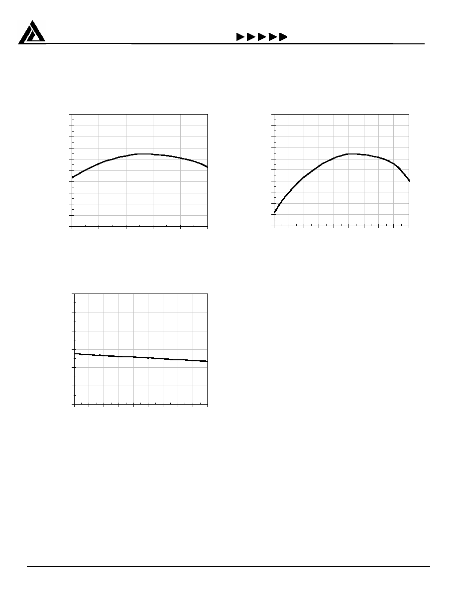
Typical DC Characteristics (nominal conditions unless specified otherwise)
Nominal Conditions: C
IN
= 1µF, C
OUT
= 2.2µF, No C
BYP
, V
IN
= 4.0V, Load = 5mA (all plots measured with 3.0V V
OUT
)
Load Regulation
2.90
2.95
3.00
3.05
3.10
0
100
200
300
400
500
600
700
LOAD CURRENT [m A]
OU
T
P
U
T
VOLT
AGE [
V
]
Dropout Voltage (V
OUT
=2.9V)
0
100
200
300
400
500
600
700
800
0
200
400
600
LOAD [mA]
DRO
P
O
UT
[
V
]
Foldback Current Limiting
0.0
1.0
2.0
3.0
4.0
0
100 200 300 400 500 600 700 800 900
LOAD CURRENT [mA]
O
U
T
P
U
T
VO
L
T
AG
E [V]
Line Regulation
2.80
2.85
2.90
2.95
3.00
3.05
3.10
2.8
3.2
3.6
4.0
4.4
4.8
5.2
5.6
6.0
INPUT VOLTAGE [V
]
O
U
T
P
U
T
VO
L
T
AG
E [
V
]
1mA Load
500m A Load
Line Regulation
0.0
0.5
1.0
1.5
2.0
2.5
3.0
3.5
4.0
0
1
2
3
4
5
6
INPUT VOLTAGE [V]
O
O
U
T
P
U
T
VO
L
T
AG
E [
V
]
1mA Load
Enable Voltage Threshold
500
600
700
800
900
1000
2
3
4
5
6
7
SUPPLY VOLTAGE [V]
T
H
R
ESH
O
L
D
[m
V]
Supply Current vs. Voltage (EN = V
IN
)
0
20
40
60
80
100
120
140
160
180
200
0
1
2
3
4
5
6
INPUT VOLTAGE [V]
G
R
O
UND CURRE
NT [
u
A
]
1mA Load
En = Vin
Ground Current vs. Output Load
100
125
150
175
200
0
100 200 300 400 500 600 700 800
LOAD CURRENT [mA]
G
R
O
UND CURRE
NT [
u
A
]
Output Supply Current vs. Voltage
0
500
1000
1500
2000
2500
0
1
2
3
4
5
6
OUTPUT SUPPLY VOLTAGE [V]
O
U
T
P
UT
S
U
P
P
L
Y
CURRE
NT
[
n
A
]
Vin = 0V, EN = 0V

CALIFORNIA MICRO DEVICES
Preliminary
CM3019
© 2004 California Micro Devices Corp. All rights reserved
02/20/04
430 N. McCarthy Blvd, Milpitas, California 95035 Tel: (408) 263-3214 Fax: (408) 263-7846 www.calmicro.com
5
Input Supply Current vs. Voltage
0
500
1000
1500
2000
2500
0
1
2
3
4
5
6
INPUT SUPPLY VOLTAGE [V]
INP
U
T S
U
P
P
L
Y
CURRE
NT [n
A
]
Vout = 0V, EN = 0V
Input Supply Current vs. Voltage
0
500
1000
1500
2000
2500
0
1
2
3
4
5
6
INPUT SUPPLY VOLTAGE [V]
I
N
P
U
T S
U
P
P
L
Y
CURRE
NT [
n
A
]
Vout = 3V, EN = 0V
Output Supply Current vs. Voltage
0
1
10
100
1000
10000
0
1
2
3
4
5
6
OUTPUT SUPPLY VOLTAGE [V]
O
U
T
P
UT
S
U
P
P
L
Y
CURRE
NT
[
u
A
]
Vin = 3V,
EN = 0V
Clamp to GND
Protect
Transient Characteristics (nominal conditions unless specified otherwise)
Nominal Conditions: C
IN
= 1µF, C
OUT
= 2.2µF, No C
BYP
, V
IN
= 4.0V, Load = 5mA (all plots measured with 3.0V V
OUT
)
10% to 90% Load Step (t
r
=1
µ
s)
10% to 90% Load Step (t
r
=1
µ
s)
10% to 90% Load Step (t
r
=1
µ
s)
3.5V ≠ 4.5V Line Step (t
r
=1
µ
s)
3.5V ≠ 4.5V Line Step (t
r
=1
µ
s)
3.5V ≠ 4.5V Line Step (t
r
=1
µ
s)
Enable Response
Enable Response
Disable Response

CALIFORNIA MICRO DEVICES
Preliminary
CM3019
© 2004 California Micro Devices Corp. All rights reserved
02/20/04
430 N. McCarthy Blvd, Milpitas, California 95035 Tel: (408) 263-3214 Fax: (408) 263-7846 www.calmicro.com
6
Power-up
Power-up
Power-down
Power Supply Ripple Rejection and Noise (nominal conditions unless specified otherwise)
Nominal Conditions: C
IN
= 1µF, V
IN
= 4.0V, PSRR measured with 50mV pk-pk sin wave on V
IN
.
(all plots measured with 3.0V V
OUT
)
Pow er Supply Ripple Reje ction [dB]
0
10
20
30
40
50
60
70
80
90
10
100
1000
10000
100000
Fre que ncy [Hz]
P
S
RR[
dB]
500mA Load
100mA Load
100uA Load
5mA Load
Cout=10uF, Cbyp=100nF
Power Supply Ripple Rejection [dB]
0
10
20
30
40
50
60
70
80
90
10
100
1000
10000
100000
Frequency [Hz]
P
S
RR [
d
B]
500mA Load
100mA Load
100uA Load
5mA Load
Cout=2.2uF, Cbyp=100nF

CALIFORNIA MICRO DEVICES
Preliminary
CM3019
© 2004 California Micro Devices Corp. All rights reserved
02/20/04
430 N. McCarthy Blvd, Milpitas, California 95035 Tel: (408) 263-3214 Fax: (408) 263-7846 www.calmicro.com
7
Power Supply Ripple Rejection [dB]
0
10
20
30
40
50
60
70
80
90
10
100
1000
10000
100000
Frequency [Hz]
P
S
RR [dB]
500mA Load
100mA Load
100uA Load
5mA Load
NO OUTPUT CAP, Cbyp=100nF
Ouput noise spectral density (100uA Load)
1.E-08
1.E-07
1.E-06
1.E+01
1.E+02
1.E+03
1.E+04
1.E+05
Frequency [Hz]
E
n
[uV
/
r
ootHz
]
Cout = 10uF, Cbyp = 100nF
CALIFORNIA MICRO DEVICES
Preliminary
CM3019
© 2004 California Micro Devices Corp. All rights reserved
02/20/04
430 N. McCarthy Blvd, Milpitas, California 95035 Tel: (408) 263-3214 Fax: (408) 263-7846 www.calmicro.com
8
Typical Thermal Characteristics (nominal conditions unless specified otherwise)
Nominal Conditions: CIN = 1uF, COUT = 2.2uF, No CBYP, VIN = 4.0V, Load = 5mA (all plots measured with 3.0V Vout)
V
OUT
vs. Temperature
-50
-40
-30
-20
-10
0
10
20
30
40
50
0
25
50
75
100
125
TEMPERATURE [
o
C]
OUTPUT CHANGE [
m
V]
V
OUT
vs. Temperature
-50
-40
-30
-20
-10
0
10
20
30
40
50
-40 -20
0
20
40
60
80 100 120 140
TEMPERATURE [
o
C]
O
U
T
P
U
T
C
H
A
N
G
E
[mV
]
I
GND
vs. Temperature
0
50
100
150
200
250
300
-40 -20
0
20
40 60
80 100 120 140
TEMPERATURE [
o
C]
GROUND CURRENT [
u
A]