©
2004 California Micro Devices Corp. All rights reserved.
08/16/04
430 N. McCarthy Blvd., Milpitas, CA 95035-5112
Tel: 408.263.3214
Fax: 408.263.7846
www.calmicro.com
1
CM3065
PRELIMINARY
2.0 Amp Tri-Mode Low Dropout CMOS Regulator
Features
∑
Operates as an adjustable output or a fixed output
regulator with 2 output voltage options
∑
1.8V or 2.5V fixed output voltage versions
∑
360mV dropout at 2.0A load current
∑
Operates from 2.2V to 5.5V input supply
∑
Low Ground current (350
µA at 2.0A Load)
∑
Stable with low ESR ceramic output capacitor
∑
Current limit protection
∑
Thermal overload protection
∑
Reverse voltage protection
∑
Thermally enhanced 8-lead SOIC or 3-lead TO-
263 package
∑
Lead-free versions available
Applications
∑
Low voltage "Core" processors
∑
Graphics cards
∑
Gigabit NIC cards
∑
PC motherboards
∑
Notebook computers
Product Description
The CM3065 family of very low dropout regulators
offers both fixed/adjustable-output and fixed-output
operation capable of delivering up to 2A of current. The
CM3065 devices are fully protected, offering overload
current limiting, short circuit protection, high tempera-
ture thermal shutdown, and reverse voltage protection
to minimize reverse current flow into the output pin.
The CM3065-xxSA/SF (8-lead, SOIC packaged)
devices operate in either adjustable or fixed output
modes. When the ADJ input is grounded, the regulator
operates as a fixed output voltage device at the speci-
fied output voltage. When the ADJ input is connected
to an external resistor network the device operates as
an adjustable regulator. The ADJ input can also be tied
directly to the OUT pin which configures the CM3065
as a 1.2V regulator. The CM3065-xxSA/SF devices
feature an Enable control input (EN), which when set
low, disables the device to a low quiescent current
mode.
The CM3065-xxTO/TN (TO-263 packaged) versions
operate as higher power, fixed output voltage devices
and are available with 1.8V or 2.5V outputs voltages
only.
The CM3065 is available in a space saving, 8-lead
power SOIC which has been thermally enhanced with
an integral leadframe to ensure maximum junction to
ambient power dissipation, or a 3-lead TO-263 pack-
age. Both packages are offered with optional lead-free
finishing.
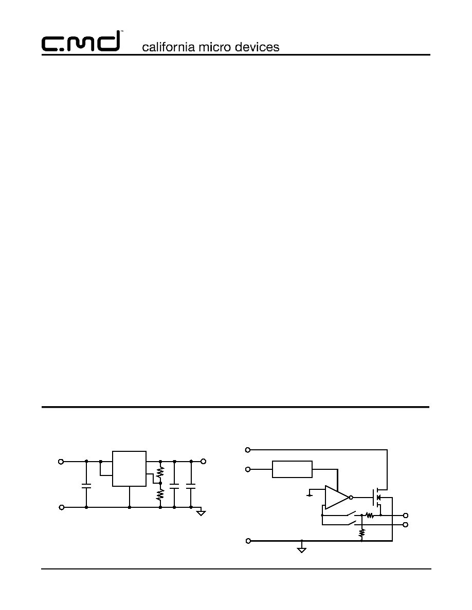
Simplified Electrical Schematic
Typical Application Circuit
1.2V Reference
Voltage
+
IN
GND
EN
ADJ
Over Current
Short Circuit
Over Temp
-
2.2V-5.5V
Controller
Fixed Output when ADJ = GND
OUT
Automatically selects Adjustable Output
(when external resistors are present)
Fixed
Adj
130K
120K
2..0 AMP
Note 1: EN pin is internally tied to V
IN
on CM3065-xxTO/TN devices
Note 2: ADJ pin is internally tied to GND on CM3065-xxTO/TN devices.
(See notes below for TO-263 devices.)
EN
(Note 1)
(Note 2)
IN
EN
OUT
GND
10
µ
F
100
n
F
V
OUT
GND
CM3065-xxSA/SF
ADJ
V
IN
3.3V
10
µ
F
2.0A
R2
R1

©
2004 California Micro Devices Corp. All rights reserved.
2
430 N. McCarthy Blvd., Milpitas, CA 95035-5112
Tel: 408.263.3214
Fax: 408.263.7846
www.calmicro.com
08/16/04
CM3065
PRELIMINARY
Ordering Information
Note 1: TO-263 packaged parts are fixed output.
Note 2: Parts are shipped in Tape & Reel form unless otherwise specified.
PIN DESCRIPTIONS
TO-263
SOIC-8
NAME
DESCRIPTION
LEAD(S)
LEAD(S)
1
2
IN
Positive input voltage for the regulator. If this input pin is greater than 2 inches from
the main input filter, a 10
µF ceramic capacitor is recommended for adequate filtering.
2, TAB
5-8
GND
The negative reference for all voltages. Also functions as a thermal path for heat dis-
sipation.
3
3
OUT
The regulated voltage output. An output capacitor of 10
µF is recommended to mini-
mize any transient load disturbances under normal operating conditions. Additional
output capacitance can be used to further improve transient load response.
---
1
EN
Enable/shutdown input. When EN is asserted high (V
EN
1.2V), the regulator is
enabled. When EN is asserted low (V
EN
0.4V), the regulator is shut down.
---
4
ADJ
Feedback input. When ADJ is grounded, the device enters fixed voltage mode. When
ADJ is connected to an external resistor network, the device operates as an adjust-
able regulator. The Adjust pin can also be tied directly to the OUT pin which config-
ures the CM3065 as a 1.2V regulator.
PACKAGE / PINOUT DIAGRAM
Note: These drawings are not to scale.
8-lead Power SOIC
1
2
3
4
8
7
6
5
EN
IN
OUT
ADJ
GND
GND
GND
GND
TOP VIEW
3
1
2
TOP VIEW
IN
GND
OUT
3-lead TO-263
Note:
is GND
Tab (on back)
CM306
5
XX
SX
CM3
065-XXTX
PART NUMBERING INFORMATION
LEADS/
PINS
Output
Voltage
Package
Standard Finish
Lead-free Finish
Ordering Part
Number
1
Part Marking
Ordering Part
Number
1
Part Marking
8
2.5
SOIC-8
CM3065-25SA
CM3065-25SA
CM3065-25SF
CM3065-25SF
8
1.8
SOIC-8
CM3065-18SA
CM3065-18SA
CM3065-18SF
CM3065-18SF
3
2.5
TO-263
CM3065-25TO
CM3065-25TO
CM3065-25TN
CM3065-25TN
3
1.8
TO-263
CM3065-18TO
CM3065-18TO
CM3065-18TN
CM3065-18TN
©
2004 California Micro Devices Corp. All rights reserved.
08/16/04
430 N. McCarthy Blvd., Milpitas, CA 95035-5112
Tel: 408.263.3214
Fax: 408.263.7846
www.calmicro.com
3
CM3065
PRELIMINARY
Specifications
Note 1: The SOIC package used is thermally enhanced through the use of a fused integral leadframe. The power rating is based on
a printed circuit board heat spreading capability equivalent to 2 square inches of copper connected to the GND pins. Typical
multi-layer boards using power plane construction will provide this heat spreading ability without the need for additional ded-
icated copper area. (Please consult with factory for thermal evaluation assistance)
ABSOLUTE MAXIMUM RATINGS
PARAMETER
RATING
UNITS
ESD Protection (HBM)
±2000
V
Pin Voltages
IN, OUT, ADJ, EN
[GND - 0.4] to +6.0
V
Storage Temperature Range
-40 to +150
∞C
Operating Temperature Range
Ambient
Junction
-40 to +85
-40 to +150
∞C
∞C
Power Dissipation (See note 1)
Internally Limited
W
STANDARD OPERATING CONDITIONS
PARAMETER
VALUE
UNITS
V
IN
2.2 to 5.5
V
Ambient Operating Temperature Range
-40 to +85
∞C
Load Current
0 to 2000
mA
C
OUT
10
±20%
µ
F

©
2004 California Micro Devices Corp. All rights reserved.
4
430 N. McCarthy Blvd., Milpitas, CA 95035-5112
Tel: 408.263.3214
Fax: 408.263.7846
www.calmicro.com
08/16/04
CM3065
PRELIMINARY
Enable Pin Input (CM3065-xxSA only)
Adjust Pin Input (output set by external resistors, CM3065-xxSA only)
Note 1: Operating Characteristics are over Standard Operating Conditions unless otherwise specified.
Note 2: Applies for CM3065-xxSA devices only.
ELECTRICAL OPERATING CHARACTERISTICS
(SEE NOTE 1)
SYMBOL
PARAMETER
CONDITIONS
MIN
TYP
MAX
UNITS
V
OUT
Regulator Output Voltage
0mA < I
LOAD
< 2.0A, V
IN
[V
OUT
+ 0.8V],
V
ADJ
=0V
CM3065-25
2.45
2.50
2.55
V
CM3065-18
1.764
1.80
1.836
V
I
LIM
Overload Current Limit
V
OUT
> 1.2V
2.2
3.0
3.8
A
I
SC
Short Circuit Current Limit
V
OUT
< 0.2V
0.5
1.2
1.8
A
V
R LOAD
Load Regulation
V
IN
=[V
OUT
+ 0.8V], 100mA
I
LOAD
1.5A
0.2
0.4
%
V
IN
=[V
OUT
+ 0.8V], 100mA
I
LOAD
2.0A
0.3
0.6
%
V
R LINE
Line Regulation
xx
I
LOAD
= 5mA; 3.0V
V
IN
to 5.0V
0.2
0.4
%
V
DROPOUT
Dropout Voltage
I
LOAD
= 100mA
18
45
mV
I
LOAD
= 1.0A
180
450
mV
I
LOAD
= 1.5A
270
600
mV
I
LOAD
= 2.0A
360
700
mV
I
GND
Ground Current
Regulator Disabled (EN=GND); V
IN
=3.3V;
Note 2
5
30
µ
A
Regulator Enabled (EN=V
IN
=[V
OUT
+ 0.8V]);
I
LOAD
= 0mA; Note 2
325
500
µ
A
Regulator Enabled (EN=V
IN
=[V
OUT
+ 0.8V]);
I
LOAD
= 1.5A; Note 2
330
550
µ
A
Regulator Enabled (EN=V
IN
=[V
OUT
+ 0.8V]);
I
LOAD
= 2.0A; Note 2
350
600
µ
A
I
ROUT
Output Reverse Leakage
V
OUT
=3.3V; V
IN
= 0V
30
100
µ
A
T
DISABLE
T
HYST
Shutdown Temperature
Thermal Hysteresis
160
25
∞C
∞C
V
TH_EN
EN Input Threshold
Voltage
Note 2
0.4
-
1.2
V
I
EN
EN Input Leakage
Current
0V < V
EN
< 5.5V; Note 2
0.1
5
µ
A
V
TH_ADJ
ADJ Input Threshold Volt-
age
Note 2
0.1
0.2
0.3
V
I
EN
ADJ Input Leakage
Current
V
ADJ
> 1.1V; Note 2
0.1
1
µ
A

©
2004 California Micro Devices Corp. All rights reserved.
08/16/04
430 N. McCarthy Blvd., Milpitas, CA 95035-5112
Tel: 408.263.3214
Fax: 408.263.7846
www.calmicro.com
5
CM3065
PRELIMINARY
Mechanical Details
The CM3065 is available in either an 8-lead SOIC or a
3-lead TO-263 package.
SOIC-8 Mechanical Specifications
Dimensions for CM3065 devices supplied in an 8-lead
SOIC package are presented below.
For complete information on the SOIC-8 package, see
the California Micro Devices SOIC Package Informa-
tion document.
* This is an approximate number which may vary.
Package Dimensions for SOIC-8
PACKAGE DIMENSIONS
Package
SOIC
Leads
8
Dimensions
Millimeters
Inches
Min
Max
Min
Max
A
1.35
1.75
0.053
0.069
A
1
0.10
0.25
0.004
0.010
B
0.33
0.51
0.013
0.020
C
0.19
0.25
0.007
0.010
D
4.80
5.00
0.189
0.197
E
3.80
4.19
0.150
0.165
e
1.27 BSC
0.050 BSC
H
5.80
6.20
0.228
0.244
L
0.40
1.27
0.016
0.050
# per tube
100 pieces*
# per tape
and reel
2500 pieces
Controlling dimension: inches
Mechanical Package Diagrams
E
D
H
TOP VIEW
L
END VIEW
C
e
B
A
A
1
SEATING
PLANE
SIDE VIEW
1
2
3
4
8
7
6
5
Pin 1
Marking