
© 2004 California Micro Devices Corp. All rights reserved.
01/20/04
430 N. McCarthy Blvd., Milpitas, CA 95035-5112
L Tel: 408.263.3214
L Fax: 408.263.7846 L www.calmicro.com
1
CM3102
Micropower 1.2V/150mA CMOS LDO Regulator
with Power Good
Features
∑
1-5ms Power Good (PG) control signal
∑
Regulated 1.2V output
∑
150mA output current
∑
Low quiescent operating current (90
µA typical)
∑
"Zero" disable mode current
∑
Foldback current limiting protection
∑
Thermal shutdown protection
∑
Stable with low-ESR capacitors
∑
SOT23-5 package
∑
"MIC5258" pinout
∑
Lead-free version available
Applications
∑
Pentium
4 Motherboards
∑
Processor Power-up Sequencing
∑
Desktop, Notebook and Palmtop Computers
∑
PC Cards
∑
Peripheral Adapter Cards
Product Description
The CM3102 is a low quiescent current (90uA) regula-
tor that delivers up to 150mA of load current at a fixed
1.2V output. In addition, the CM3102 features a Power
Good output signal (PG) that goes open drain 1 to 5
ms after the output voltage has exceeded typically 93%
of its nominal level.
A dedicated control input (EN, Active High) has been
included for power-up sequencing flexibility. When this
input is taken low, the regulator is disabled. In this
state, the supply current will drop to near zero. An inter-
nal discharge MOSFET resistance (500
) will force the
output to ground whenever the device has been shut-
down.
The CM3102 is fully protected, offering both overload
current limiting and high temperature thermal shut-
down.
Available in a tiny SOT23 package, the device is ideal
for space critical applications.
The CM3102 is available with optional lead-free finish-
ing.
Simplified Electrical Schematic
Pentium
4 Motherboard
EN
+
IN
GND
OUT
-
V
REF
1.2V
2.5ms
+
-
V
REF
X 0.93
1X
PG
1.2V/150mA
Typical Application Circuit
Application Circuit
IN
EN
OUT
GND
.1
µ
F*
.1
µ
F
VCCVID
VCC3
CM3102-12Sx
10
PG
PG
1.2V
* Input capacitor optional.
IN
EN
OUT
GND
1
µ
F*
1
µ
F
V
OUT
GND
CM3102-12Sx
PG
47k
V
IN
PG
EN
* Input capacitor optional.

© 2004 California Micro Devices Corp. All rights reserved.
2
430 N. McCarthy Blvd., Milpitas, CA 95035-5112
L Tel: 408.263.3214
L Fax: 408.263.7846 L www.calmicro.com
01/20/04
CM3102
Ordering Information
Note 1: Parts are shipped in Tape & Reel form unless otherwise specified.
PIN DESCRIPTIONS
PIN
NAME
DESCRIPTION
1
IN
Positive input voltage for the regulator. The internal loading on this input is typically 300
µA when-
ever the regulator is enabled, and less than 1
µA when the regulator is disabled. Although an input
filter capacitor is not required, it is recommended that a 1
µF ceramic capacitor be used for addi-
tional filtering and stability if this pin is greater than 2 inches from the main input filter.
2
GND
The negative reference for all voltages.
3
EN
Enable/shutdown input. When EN is asserted high (V
EN
1.6V), the regulator is enabled. When EN
is asserted low (V
EN
0.4V), the regulator's series pass transistor is forced into a high impedance
mode and an internal discharge resistance (500
) is applied to the output to quickly reduce the out-
put voltage to 0 volts.
4
PG
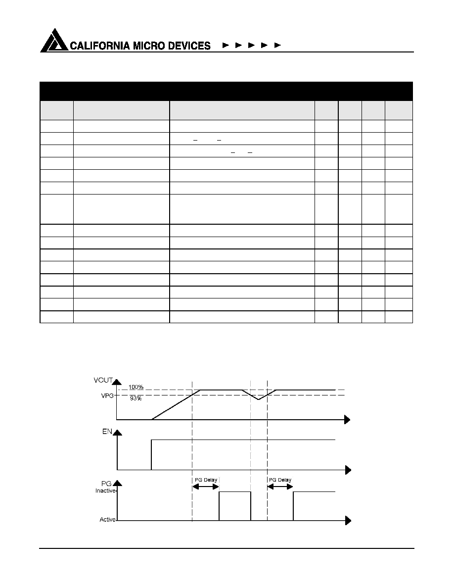
Power Good output. This is an open drain output and functions as a supply voltage supervisor for
the output voltage. It is asserted low when the output falls below 89% of its nominal value. This out-
put becomes inactive when V
OUT
remains above 97% of its nominal value for 1 to 5ms.
5
OUT
The regulated voltage output. An output capacitor of 1
µF is recommended to minimize any tran-
sient load disturbances under normal operating conditions. Additional output capacitance can be
used to further improve transient load response.
PACKAGE / PINOUT DIAGRAM
Note: This drawing is not to scale.
5-pin SOT23
IN
GND
EN
OUT
PG
1
2
5
3
4
B
A
12/BB
12
Top View
PART NUMBERING INFORMATION
Regulator
Pins
Package
Standard Finish
Lead-free Finish
Ordering Part
Number
1
Part Marking
Ordering Part
Number
1
Part Marking
CM3102-12
5
SOT23-5
CM3102-12ST
BA12
CM3102-12SO
BB12

© 2004 California Micro Devices Corp. All rights reserved.
01/20/04
430 N. McCarthy Blvd., Milpitas, CA 95035-5112
L Tel: 408.263.3214
L Fax: 408.263.7846
L www.calmicro.com
3
CM3102
Specifications
Note 1: The power rating is based on a printed circuit board heat spreading capability equivalent to 2 square inches of copper con-
nected to the GND pins. Typical multi-layer boards using power plane construction will provide this heat spreading ability
without the need for additional dedicated copper area. Please consult with factory for thermal evaluation assistance.
ABSOLUTE MAXIMUM RATINGS
PARAMETER
RATING
UNITS
ESD Protection (HBM)
+2000
V
Pin Voltages
V
IN
V
OUT
V
EN
[GND - 0.6] to +6.0
[GND - 0.6] to [V
IN
+0.6]
[GND - 0.6] to [V
IN
+0.6]
V
V
V
Storage Temperature Range
-40 to +150
∞C
Operating Temperature Range
Ambient
Junction
0 to +70
0 to +150
∞C
∞C
Power Dissipation (See note 1)
Internally Limited
W
STANDARD OPERATING CONDITIONS
PARAMETER
VALUE
UNITS
V
IN
2.7 to 5.5
V
Ambient Operating Temperature Range
0 to +70
∞C
Load Current
0 to 150
mA
C
OUT
1 +20%
µF
© 2004 California Micro Devices Corp. All rights reserved.
4
430 N. McCarthy Blvd., Milpitas, CA 95035-5112
L Tel: 408.263.3214
L Fax: 408.263.7846 L www.calmicro.com
01/20/04
CM3102
Note 1: Operating Characteristics are over Standard Operating Conditions unless otherwise specified.
Timing Diagram
ELECTRICAL OPERATING CHARACTERISTICS
(SEE NOTE 1)
SYM-
BOL
PARAMETER
CONDITIONS
MIN
TYP
MAX
UNITS
V
OUT
Regulator Output Voltage
0.1mA < I
LOAD
< 150mA
1.1
1.2
1.3
V
V
R LOAD
Load Regulation
10mA < I
LOAD
< 150mA
30
mV
V
R LINE
Line Regulation
xx
I
LOAD
= 5mA; 2.7V < V
IN
< to 3.6V
20
mV
I
LIM
Overload Current Limit
160
350
mA
I
SC
Short Circuit Current Limit
V
OUT
< 0.5V
140
mA
R
DISCH
Discharge Resistance
EN tied to GND
500
I
GND
Ground Current
Regulator Enabled (EN=V
IN
); I
LOAD
= 0mA
Regulator Enabled (EN=V
IN
); I
LOAD
= 150mA
Regulator Disabled (EN=GND); (Disable Mode)
90
100
0.01
200
250
10
µA
µA
µA
V
EN
EN Input Logic High Threshold Regulator Enabled
1.6
V
V
DIS
EN Input Logic Low Threshold
Regulator Disabled
0.4
V
I
EN
Enable Input Current
0.01
µA
V
PGL
Power Good Low Threshold
% of V
OUT
(PG ON)
89
%
V
PGH
Power Good High Threshold
% of V
OUT
(PG OFF)
97
%
V
OL
Power Good Logic "0" Voltage
I
L
=100
µA; Fault Condition
0.02
0.1
V
I
PG
Power Good Leakage Current
Power Good Off; V
PG
=5.5V
0.01
µA
PG
DELAY
Delay Time to Power Good
1
5
mS
© 2004 California Micro Devices Corp. All rights reserved.
01/20/04
430 N. McCarthy Blvd., Milpitas, CA 95035-5112
L Tel: 408.263.3214
L Fax: 408.263.7846
L www.calmicro.com
5
CM3102
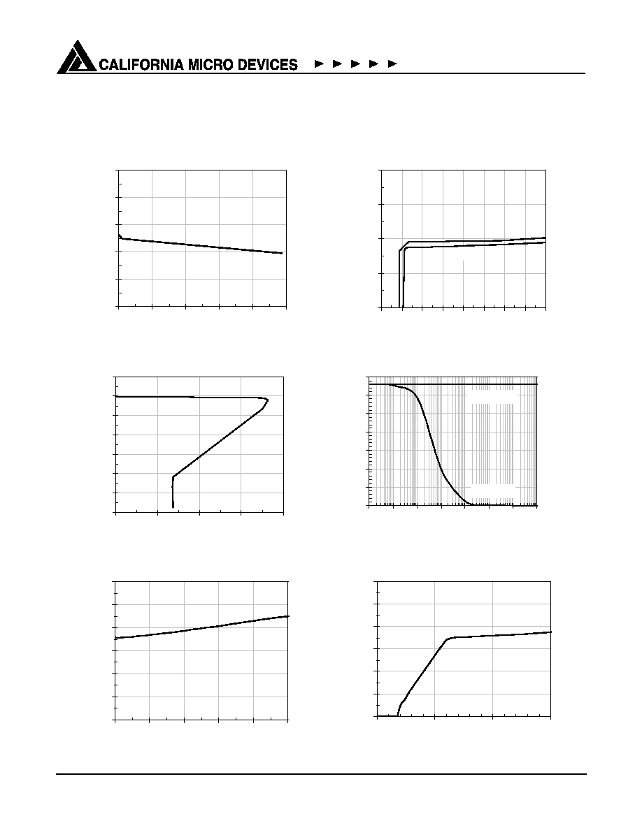
Performance Information
CM3102 Typical DC Characteristics (nominal conditions unless specified otherwise)
Load Regulation
1.15
1.17
1.19
1.21
1.23
1.25
0
50
100
150
200
250
LOAD CURRENT [mA]
OUTPUT VOLTAG
E [V]
Line Regulation (1% and 100% rated load)
1.10
1.15
1.20
1.25
1.30
2.0
2.5
3.0
3.5
4.0
4.5
5.0
5.5
6.0
INPUT VOLTAGE [V]
OUTPUT VOLTAG
E [V]
150m A
1m A
Foldback Current Protection
0.0
0.2
0.4
0.6
0.8
1.0
1.2
1.4
0
100
200
300
400
LOAD CURRENT [mA]
OUTPUT VOLTAG
E [V]
Power Good Pull-up Resistor vs.
V
PG
0.0
0.5
1.0
1.5
2.0
2.5
3.0
3.5
0.001
0.01
0.1
1
10
100
1000
10000
PULL-UP RESISTOR [k
]
POWER GOO
D VOLTAGE
[V]
Power Good
Power Fail
Ground Current vs. Load Current (V
IN
=3.3V)
0
25
50
75
100
125
150
0
50
100
150
200
250
LOAD CURRENT [mA]
GROUND CURRENT [uA]
Ground Current vs. Input Voltage (1mA Load)
0
25
50
75
100
125
150
0
2
4
6
INPUT VOLTAGE [V]
GROUND CURRENT [uA]

© 2004 California Micro Devices Corp. All rights reserved.
6
430 N. McCarthy Blvd., Milpitas, CA 95035-5112
L Tel: 408.263.3214
L Fax: 408.263.7846 L www.calmicro.com
01/20/04
CM3102
Performance Information (cont'd)
CM3102 Typical DC Characteristics (cont'd, nominal conditions unless specified otherwise)
Short Circuit Current vs. Input Voltage
0
20
40
60
80
100
120
140
160
180
2.5
3.0
3.5
4.0
4.5
5.0
5.5
6.0
INPUT VOLTAGE [V]
SHORT CIRCUIT CURRENT [mA]
Current Limit vs. Input Voltage (V
OUT
=1.15V)
0
100
200
300
400
500
600
2.5
3.0
3.5
4.0
4.5
5.0
INPUT VOLTAGE [V]
CURRENT LIMIT [mA]
Enable Voltage vs. Input Voltage
1.00
1.02
1.04
1.06
1.08
1.10
2.5
3.0
3.5
4.0
4.5
5.0
5.5
6.0
INPUT VOLTAGE [V]
ENABLE
THRESHOLD
VOLTAG
E [V]
PG
DELAY
vs. Input Voltage
0.0
0.5
1.0
1.5
2.0
2.5
3.0
3.5
4.0
4.5
5.0
INPUT VOLTAGE [V]
PG
DELAY
[ms]

© 2004 California Micro Devices Corp. All rights reserved.
01/20/04
430 N. McCarthy Blvd., Milpitas, CA 95035-5112
L Tel: 408.263.3214
L Fax: 408.263.7846
L www.calmicro.com
7
CM3102
Performance Information (cont'd)
CM3102 Transient Characteristics (nominal conditions unless specified otherwise)
(PG connected to V
IN
with a 47k
resistor)
Load transient (10% to 90%) Step Response
(V
IN
= 3.3V, C
IN
= C
OUT
= 1uF Ceramic)
Line Transient (0.6Vpp) Step Response
(1mA Load, C
OUT
= 1uF Cerami
c, no C
IN
)
Enable Response
(150mA Load, C
IN
= C
OUT
= 1uF Ceramic)
Cold Start & Power Down
(150mA Load, C
IN
= C
OUT
= 1uF Ceramic)

© 2004 California Micro Devices Corp. All rights reserved.
8
430 N. McCarthy Blvd., Milpitas, CA 95035-5112
L Tel: 408.263.3214
L Fax: 408.263.7846 L www.calmicro.com
01/20/04
CM3102
Performance Information (cont'd)
CM3102-12ST/SO Typical Thermal Characteristics
The overall junction to ambient thermal resistance
(
JA
) for device power dissipation (PD) consists prima-
rily of two paths in series. The first path is the junction
to the case (
JC
) which is defined by the package style,
and the second path is case to ambient (
CA
) thermal
resistance which is dependent on board layout. The
final operating junction temperature for any set of con-
ditions can be estimated by the following thermal equa-
tion:
T
JUNC
= T
AMB
+ P
D
(
JC
) + P
D
(
CA
)
= T
AMB
+ P
D
(
JA
)
The CM3102-12ST/SO uses a SOT23-5 package.
When this package is mounted on a double sided
printed circuit board with two square inches of copper
allocated for "heat spreading", the resulting
JA
is
175∞C/W.
Based on a maximum power dissipation of 315mW
(2.1Vx150mA), with an ambient of 70∞C the resulting
junction temperature will be:
T
JUNC
=
T
AMB
+ P
D
(
JA
)
= 70∞C + 315mW X (175∞C/W)
= 70∞C + 55∞C = 125∞C
Thermal characteristics were measured using a double
sided board with two square inches of copper area
connected to the GND pin for "heat spreading".
Measurements showing performance up to junction
temperature of 125∞C were performed under light load
conditions (1mA). This allows the ambient temperature
to be representative of the internal junction tempera-
ture.
Note: The use of multi-layer board construction with
separate ground and power planes will further enhance
the overall thermal performance. In the event of no
copper area being dedicated for heat spreading, a
multi-layer board construction, using only the minimum
size pad layout, will provide the CM3102-12ST/SO with
an overall
JA
of 175∞C/W which allows up to 450mW
to be safely dissipated for the maximum junction tem-
perature.
V
OUT
Variation with T
AMB
(150mA Load)
1.170
1.180
1.190
1.200
1.210
1.220
1.230
-25
0
25
50
75
AMBIENT TEMPERATURE [
o
C]
OUTPUT VOLTAG
E
[V]
V
OUT
Variation with T
JUNCT
(1mA Load)
1.170
1.180
1.190
1.200
1.210
1.220
1.230
-25
0
25
50
75
100
125
JUNCTION TEMPERATURE [
o
C]
OUTPUT VOLTAG
E [V]
Short Circuit Current vs. T
JUNCT
0
50
100
150
200
-50
-25
0
25
50
75
100
125
JUNCTION TEMPERATURE [
o
C]
SHORT CIRCUIT CURRENT [mA]
© 2004 California Micro Devices Corp. All rights reserved.
01/20/04
430 N. McCarthy Blvd., Milpitas, CA 95035-5112
L Tel: 408.263.3214
L Fax: 408.263.7846
L www.calmicro.com
9
CM3102
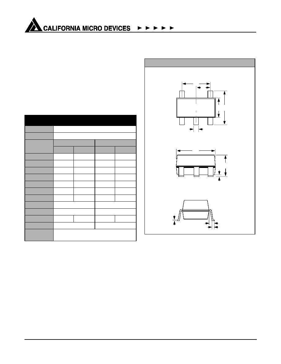
Mechanical Details
SOT23-5 Mechanical Specifications
Dimensions for CM3102-12ST/SO device packaged in
5-pin SOT23 package are presented below.
For complete information on the SOT23-5 package,
see the California Micro Devices SOT23 Package Infor-
mation document.
Package Dimensions for SOT23-5.
PACKAGE DIMENSIONS
Package
SOT23-5 (JEDEC name is MO-178)
Pins
5
Dimensions
Millimeters
Inches
Min
Max
Min
Max
A
--
1.45
--
0.0571
A1
0.00
0.15
0.0000
0.0059
b
0.30
0.50
0.0118
0.0197
c
0.08
0.22
0.0031
0.0087
D
2.75
3.05
0.1083
0.1201
E
2.60
3.00
0.1024
0.1181
E1
1.45
1.75
0.0571
0.0689
e
0.95 BSC
0.0374 BSC
e1
1.90 BSC
0.0748 BSC
L
0.30
0.60
0.0118 0.0236
L1
0.60 REF
0.0236 REF
# per tape
and reel
3000 pieces
Mechanical Package Diagrams
TOP VIEW
5
4
e1
e
E1 E
b
A
SIDE VIEW
D
A1
L1
END VIEW
c
L
1
2
3