
© 2004 California Micro Devices Corp. All rights reserved.
01/28/04
430 N. McCarthy Blvd., Milpitas, CA 95035-5112
L Tel: 408.263.3214
L Fax: 408.263.7846 L www.calmicro.com
1
CM3103
400mA SmartOR
TM
Regulator with V
AUX
Switch
Features
∑
Continuous 3.3V / 400mA output from two inputs
∑
Complete Power Management solution
∑
Built-in hysteresis when selecting input supplies
∑
Integrated switch featuring low RDS
ON
(0.25
typ.
)
∑
Foldback current limiting protection
∑
Thermal overload shutdown protection
∑
8-pin SOIC package
∑
Lead-free version available
Applications
∑
PCI adapter cards with Wake-On-LAN
∑
Network Interface Cards (NICs)
∑
Multiple power supply systems
∑
Systems with standby capabilities
Product Description
The CM3103 combines a fixed voltage regulator and a
V
AUX
switch in a single 8-pin SOIC package. The volt-
age regulator is capable of delivering up to 400mA con-
tinuously at 3.3V. The output power is provided from
two independent input voltage sources on a prioritized
basis. Power is always taken in priority of V
CC
, then
V
AUX
.
When V
CC
(5V) is present, the device automatically
enables the regulator, producing a stable 3.3V output
at V
OUT
, while disabling the V
AUX
switch.
When only V
AUX
(3.3V) is present, the device provides
a low impedance direct connection (0.25
typ.) from
V
AUX
to V
OUT
.
All the necessary control circuitry needed to provide a
smooth and automatic transition between both supplies
has been incorporated. This allows the V
CC
input sup-
ply to be dynamically switched without loss of output
voltage.
The CM3103 is available with optional lead-free finish-
ing.
Simplified Electrical Schematic
Typical Application Circuit
+
V
CC
GND
V
OUT
-
+
Enable
-
Controller
AuxSw
3.3V
4.2V
Vdeselect
AuxSw
0.25
Regulator Amp
V
AUX
V
AUX
V
OUT
GND
V
OUT
CM3103
V
CC
10
µ
F
5V
V
CC
V
AUX
3.3V
C
EXT
+
GND
1
µ
F
C
IN
+
3.3V/400mA
© 2004 California Micro Devices Corp. All rights reserved.
2
430 N. McCarthy Blvd., Milpitas, CA 95035-5112
L Tel: 408.263.3214
L Fax: 408.263.7846 L www.calmicro.com
01/28/04
CM3103
Ordering Information
Note 1: Parts are shipped in Tape & Reel form unless otherwise specified.
PIN DESCRIPTIONS
PIN(S)
NAME
DESCRIPTION
1
N.C.
2
V
CC
Positive input supply for the voltage regulator. Whenever this supply voltage exceeds the V
CCSEL
level (4.4V), it will immediately be given priority and be used to power the regulator output. If this
supply voltage falls below the V
CCDES
level (4.2V) it will immediately be deselected and no longer
provide power for the regulator output. An internal hysteresis voltage of 0.2V is used to prevent any
chatter during selection and deselection of V
CC
. The effective source impedance of V
CC
should be
kept below 0.3 ohm to ensure changeover disturbances do not exceed the hysteresis level.
If the connection to V
CC
is made within a few inches of the main input filter, a bypass capacitor may
not be necessary. Otherwise a bypass filter capacitor in the range of 1
µF to 10µF will ensure ade-
quate filtering.
3
V
OUT
Regulator output. Power is provided from the regulator or via the low impedance auxiliary switch.
This output requires a capacitance of 10
µF to ensure regulator stability and minimize the peak out-
put disturbance during power supply changeover.
4
V
AUX
Auxiliary voltage power source. This supply is selected only when V
CC
falls below 4.2V. Under
these conditions an internal switch that provides a very low impedance connection directly between
V
OUT
and V
AUX
is enabled .
5-8
GND
The negative reference for all voltages. Also functions as a thermal path for heat dissipation.
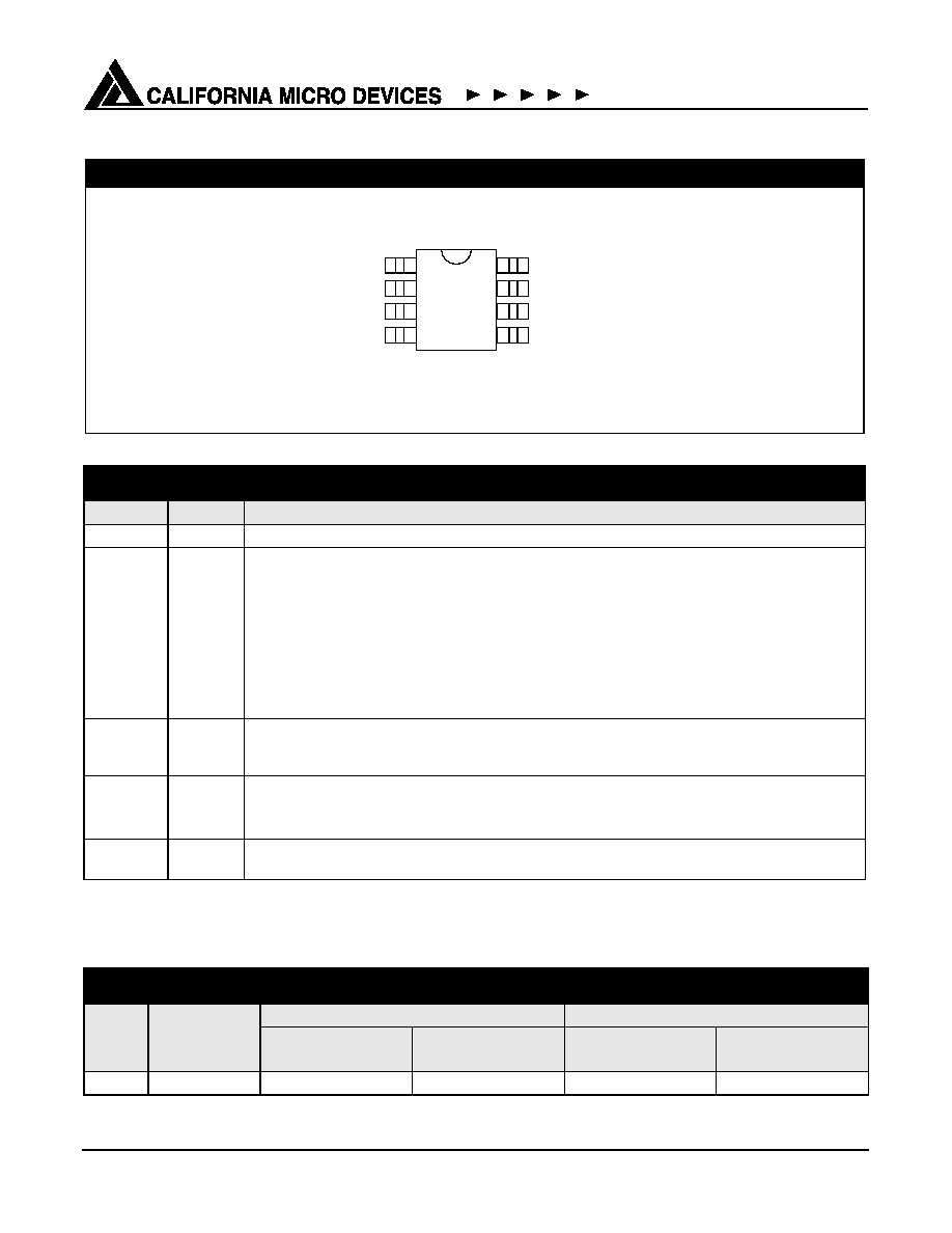
PACKAGE / PINOUT DIAGRAM
Note: This drawing is not to scale.
8-pin Power SOIC
1
2
3
4
8
7
6
5
N.C.
V
CC
V
OUT
V
AUX
GND
GND
GND
GND
TOP VIEW
PART NUMBERING INFORMATION
Pins
Package
Standard FInish
Lead-free Finish
Ordering Part
Number
1
Part Marking
Ordering Part
Number
1
Part Marking
8
Power SOIC
CM3103-01SA
CM3103SA
CM3103-01SF
CM3103SF

© 2004 California Micro Devices Corp. All rights reserved.
01/28/04
430 N. McCarthy Blvd., Milpitas, CA 95035-5112
L Tel: 408.263.3214
L Fax: 408.263.7846
L www.calmicro.com
3
CM3103
Specifications
Note 1: At rated load, the power dissipation will be 0.68Watt (1.7V x 0.4A). Under these conditions, (in a 70∞C ambient), the thermal
resistance from junction to ambient (
JA
) must not exceed 80∞C/W. This is typically achieved with 2 square inches of copper
printed circuit board area connected to the GND pins for heat spreading, or equivalent.
ABSOLUTE MAXIMUM RATINGS
PARAMETER
RATING
UNITS
ESD Protection (HBM)
+2000
V
Pin Input Voltages
V
CC
V
AUX
[GND - 0.5] to +6.0
[GND - 0.5] to +4.0
V
V
Storage Temperature Range
-40 to +150
∞C
Operating Temperature Range
Ambient
Junction
0 to +70
0 to +125
∞C
∞C
Power Dissipation (See Note 1)
Internally Limited
W
STANDARD OPERATING CONDITIONS
PARAMETER
VALUE
UNITS
V
CC
5.0 +0.25
V
V
AUX
3.3 +0.3
V
Ambient Operating Temperature Range
0 to +70
∞C
Load Current
0 to 400
mA
C
EXT
10 +20%
µF

© 2004 California Micro Devices Corp. All rights reserved.
4
430 N. McCarthy Blvd., Milpitas, CA 95035-5112
L Tel: 408.263.3214
L Fax: 408.263.7846 L www.calmicro.com
01/28/04
CM3103
Note 1: Operating characteristics are over Standard Operating Conditions unless otherwise specified.
Note 2: The disturbance on V
CC
during supply changeover should be kept below the hysteresis voltage to prevent any chatter. The
source resistance on the V
CC
supply should be kept to less than 0.3 ohms to ensure precise switching.
ELECTRICAL OPERATING CHARACTERISTICS
(SEE NOTE 1)
SYMBOL
PARAMETER
CONDITIONS
MIN
TYP
MAX
UNITS
V
OUT
Regulator Output Voltage
0mA < I
LOAD
< 400mA
3.135
3.300
3.465
V
I
LIM
Regulator Current Limit
V
OUT
> 0V
410
500
mA
I
S/C
Short Circuit Current
V
CC
=5V, V
OUT
< 0V
150
mA
V
R LOAD
Load Regulation
V
CC
=5V, 5mA < I
LOAD
< 400mA
20
mV
V
R LINE
Line Regulation
xx
I
LOAD
= 5mA; 4.5V < V
IN
< to 5.5V
2
mV
V
CCSEL
V
CC
Select Voltage
V
AUX
present
4.40
4.60
V
V
CCDES
V
CC
Deselect Voltage
V
AUX
present
4.00
4.20
V
V
HYST
Hysteresis Voltage
V
AUX
present; See Note 2
0.20
V
R
SW
V
AUX
Switch Resistance
0.25
0.40
I
RCC
I
RAUX
V
CC
Reverse Leakage
V
AUX
Reverse Leakage
One supply input taken to GND while the others
remain at nominal voltage.
5
100
µA
I
CC
V
CC
Supply Current
V
CC
> V
CCSEL
, I
LOAD
=0mA
0.8
1.5
mA
I
AUX
V
AUX
Supply Current
V
AUX
is selected, I
LOAD
=0mA
0.20
0.30
mA
I
GND
Ground Current
V
AUX
is selected, (V
CC/SBY
= 0V)
V
CC/SBY
= 5V, I
LOAD
= 0mA
V
CC/SBY
= 5V, I
LOAD
= 400mA
0.20
0.80
1.00
0.30
1.50
2.00
mA
mA
mA
T
DISABLE
T
HYST
Shutdown Temperature
Thermal Hysteresis
160
20
∞C
∞C

© 2004 California Micro Devices Corp. All rights reserved.
01/28/04
430 N. McCarthy Blvd., Milpitas, CA 95035-5112
L Tel: 408.263.3214
L Fax: 408.263.7846
L www.calmicro.com
5
CM3103
Performance Information
CM3103 Typical DC Characteristics (nominal conditions unless specified otherwise)
VCC Supply Current vs. Voltage
0.0
0.1
0.2
0.3
0.4
0.5
0.6
0.7
0.8
0.9
1.0
0
1
2
3
4
5
6
VCC Input Voltage [V]
Supply Current [mA]
VAUX Supply Current vs. Voltage
0.0
0.1
0.2
0.3
0.4
0.5
0
1
2
3
4
VAUX Input Voltage [V]
Supply Current [
mA]
Ground Current vs. Output Load
0.6
0.7
0.8
0.9
1.0
1.1
1.2
0
100
200
300
400
Load Current [mA]
Ground Current [mA]
Line Regulation
3.0
3.1
3.2
3.3
3.4
3.5
4
4.5
5
5.5
6
Line Voltage [V]
Regulator Output Voltage [V]
5mA
400mA

© 2004 California Micro Devices Corp. All rights reserved.
6
430 N. McCarthy Blvd., Milpitas, CA 95035-5112
L Tel: 408.263.3214
L Fax: 408.263.7846 L www.calmicro.com
01/28/04
CM3103
Performance Information (cont'd)
CM3103 Typical DC Characteristics (cont'd, nominal conditions unless specified otherwise)
Load Regulation (5V supply)
3.15
3.20
3.25
3.30
3.35
3.40
3.45
0
100
200
300
400
500
Load Current [mA]
Regulator Output Voltage [V]
Foldback Current Limit Protection
0.0
0.5
1.0
1.5
2.0
2.5
3.0
3.5
4.0
0
100
200
300
400
500
600
Output Current [mA]
Regulator Output Voltage [V]
Regulator Dropout Characteristics
0.0
0.2
0.4
0.6
0.8
1.0
1.2
0
100
200
300
400
Load Current [mA]
Dropout Voltage [V]
Switch Resistance vs. VAUX supply
0.20
0.25
0.30
0.35
0.40
3.0
3.1
3.2
3.3
3.4
3.5
3.6
VAUX Input Voltage [V]
ON Resistance [
[]
© 2004 California Micro Devices Corp. All rights reserved.
01/28/04
430 N. McCarthy Blvd., Milpitas, CA 95035-5112
L Tel: 408.263.3214
L Fax: 408.263.7846
L www.calmicro.com
7
CM3103
Performance Information (cont'd)
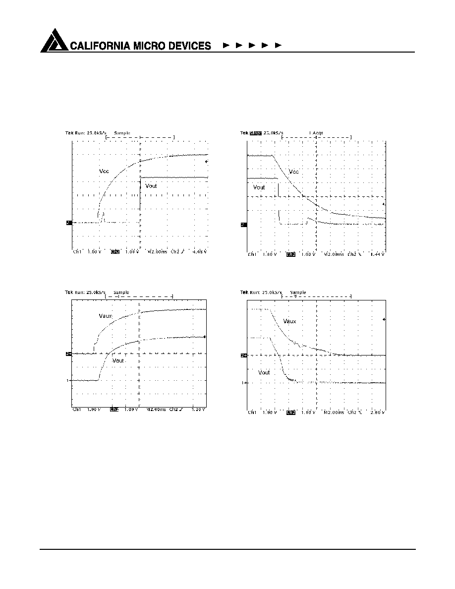
CM3103 Transient Characteristics (nominal conditions unless specified otherwise)
(V
CC
source resistance set to 0.2
)
V
CC
Cold Start (Load = 400mA)
V
CC
Full Power Down (Load = 400mA)
V
AUX
Cold Start (Load = 400mA)
V
AUX
Full Power Down (Load = 400mA)

© 2004 California Micro Devices Corp. All rights reserved.
8
430 N. McCarthy Blvd., Milpitas, CA 95035-5112
L Tel: 408.263.3214
L Fax: 408.263.7846 L www.calmicro.com
01/28/04
CM3103
Performance Information (cont'd)
CM3103 Transient Characteristics (cont'd; nominal conditions unless specified otherwise)
(V
CC
source resistance set to 0.2
)
V
CC
power up (V
AUX
= 3.3V, Load = 300mA)
V
CC
power down (V
AUX
= 3.3V, Load = 300mA)
Load Transient Response (10% - 90% rated)
Line Transient (1Vpp) Response

© 2004 California Micro Devices Corp. All rights reserved.
01/28/04
430 N. McCarthy Blvd., Milpitas, CA 95035-5112
L Tel: 408.263.3214
L Fax: 408.263.7846
L www.calmicro.com
9
CM3103
Performance Information (cont'd)
CM3103 Typical Thermal Characteristics
The overall junction to ambient thermal resistance
(
JA
) for device power dissipation (P
D
) consists prima-
rily of two paths in series. The first path is the junction
to the case (
JC
) which is defined by the package style,
and the second path is case to ambient (
CA
) thermal
resistance which is dependent on board layout. The
final operating junction temperature for any set of con-
ditions can be estimated by the following thermal equa-
tion:
T
JUNC
= T
AMB
+ P
D
(
JC
) + P
D
(
CA
)
= T
AMB
+ P
D
(
JA
)
The CM3103 uses a thermally enhanced package
where all the GND pins (5 through 8) are integral to the
leadframe. When this package is mounted on a double-
sided printed circuit board with two square inches of
copper allocated for "heat spreading", the resulting
JA
is about 50∞C/W.
Based on a typical operating power dissipation of 0.7W
(1.75V x 0.4A) with an ambient of 70∞C, the resulting
junction temperature will be:
T
JUNC
= T
AMB
+ P
D
(
JA
)
= 70∞C + 0.7W X (50∞C/W)
= 70∞C + 35∞C = 105∞C
Thermal characteristics were measured using a double-
sided board with two square inches of copper area con-
nected to the GND pin for "heat spreading".
Measurements showing performance up to junction
temperature of 125∞C were performed under light load
conditions (5mA). This allows the ambient temperature
to be representative of the internal junction tempera-
ture.
Note: The use of multi-layer board construction with
separate ground and power planes will further enhance
the overall thermal performance. In the event of no
copper area being dedicated for heat spreading, a
multi-layer board construction, using only the minimum
size pad layout, will provide the CM3103 with an overall
JA
of 70∞C/W which allows up to 780mW to be safely
dissipated for the maximum junction temperature.
V
OUT
Variation with T
AMB
(400mA Load)
3.28
3.29
3.30
3.31
3.32
20
30
40
50
60
70
Temperature [
o
C]
Regulator Output Voltage [
V
Select/Deselect Threshold Variation with T
JUNCT
4.20
4.25
4.30
4.35
4.40
4.45
4.50
4.55
25
50
75
100
125
150
Temperature [
o
C]
Threshold Voltage [V
]
Vselect
Vdeselect
V
AUX
Switch Resistance vs T
AMB
0.25
0.27
0.29
0.31
0.33
0.35
0.37
20
30
40
50
60
70
Temperature [
o
C]
On Resistance [
]

© 2004 California Micro Devices Corp. All rights reserved.
10
430 N. McCarthy Blvd., Milpitas, CA 95035-5112
L Tel: 408.263.3214
L Fax: 408.263.7846 L www.calmicro.com
01/28/04
CM3103
Mechanical Details
SOIC-8 Mechanical Specifications
Dimensions for CM3103 devices packaged in 8-pin
SOIC packages are presented below.
For complete information on the SOIC-8 package, see
the California Micro Devices SOIC Package Informa-
tion document.
* This is an approximate number which may vary.
Package Dimensions for SOIC-8
PACKAGE DIMENSIONS
Package
SOIC
Pins
8
Dimensions
Millimeters
Inches
Min
Max
Min
Max
A
1.35
1.75
0.053
0.069
A
1
0.10
0.25
0.004
0.010
B
0.33
0.51
0.013
0.020
C
0.19
0.25
0.007
0.010
D
4.80
5.00
0.189
0.197
E
3.80
4.19
0.150
0.165
e
1.27 BSC
0.050 BSC
H
5.80
6.20
0.228
0.244
L
0.40
1.27
0.016
0.050
# per tube
100 pieces*
# per tape
and reel
2500 pieces
Controlling dimension: inches
Mechanical Package Diagrams
E
D
H
TOP VIEW
L
END VIEW
C
e
B
A
A
1
SEATING
PLANE
SIDE VIEW
1
2
3
4
8
7
6
5
Pin 1
Marking