© 2004 California Micro Devices Corp. All rights reserved.
02/02/04
430 N. McCarthy Blvd., Milpitas, CA 95035-5112
L Tel: 408.263.3214 L Fax: 408.263.7846 L www.calmicro.com
1
CM3106
2 Amp Source/ Sink Bus Termination Regulator
Features
∑
Ideal for DDR-I and DDR-II V
TT
applications
∑
Sinks and sources 2.0A for DDR-I
∑
Over current protection
∑
Over temperature protection
∑
Integrated power MOSFETs
∑
Excellent accuracy (0.5% load regulation)
∑
Pin and functionally compatible with LP2995
∑
8-lead SOIC and PSOP packages
∑
Lead-free versions available
Applications
∑
Single and Dual Channel DDR Memory
Bus Termination
∑
Active Termination Buses
∑
Graphics Card Memory Termination
Product Description
The CM3106 is a sinking and sourcing regulator specif-
ically designed for providing power to DDR memory
terminating resistors and companion chip set V
TT
power. The output voltage accurately tracks V
DDQ
/2.
The CM3106 can source and sink current up to 2A,
ideal for DDR-I memory systems, and 1.2A for DDR-II
systems, while maintaining a load regulation of 0.5% in
either application.
The CM3106 provides over current and over tempera-
ture protection which protects the device from exces-
sive heating due to high current and high temperature.
A shutdown capability using an external transistor
reduces power consumption and provides a high
impedance output.
The CM3106 is housed in both 8-lead SOIC and PSOP
packages and is available with optional lead-free finish-
ing.
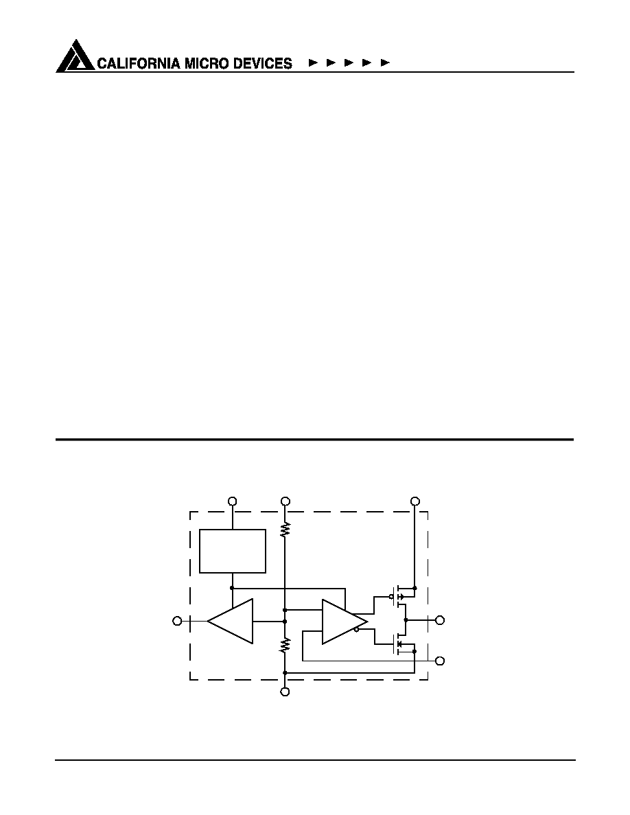
Simplified Electrical Schematic
V
REF
AV
IN
GND
Over Current
V
SENSE
50
K
Over Temp
Reference
IN
OUT
Buffer
V
TT
Driver
50K
V
DDQ
PV
IN
© 2004 California Micro Devices Corp. All rights reserved.
2
430 N. McCarthy Blvd., Milpitas, CA 95035-5112
L Tel: 408.263.3214 L Fax: 408.263.7846 L www.calmicro.com
02/02/04
CM3106
Ordering Information
Note 1: Parts are shipped in Tape & Reel form unless otherwise specified.
PIN DESCRIPTIONS
LEAD(S)
NAME
DESCRIPTION
1
NC
No Connect
2
GND
Ground
3
V
SENSE
Feedback
4
V
REF
Reference Output, VDDQ/2
5
V
DDQ
V
DDQ
Input
6
AV
IN
Analog Input
7
PV
IN
Power Input
8
V
TT
Output
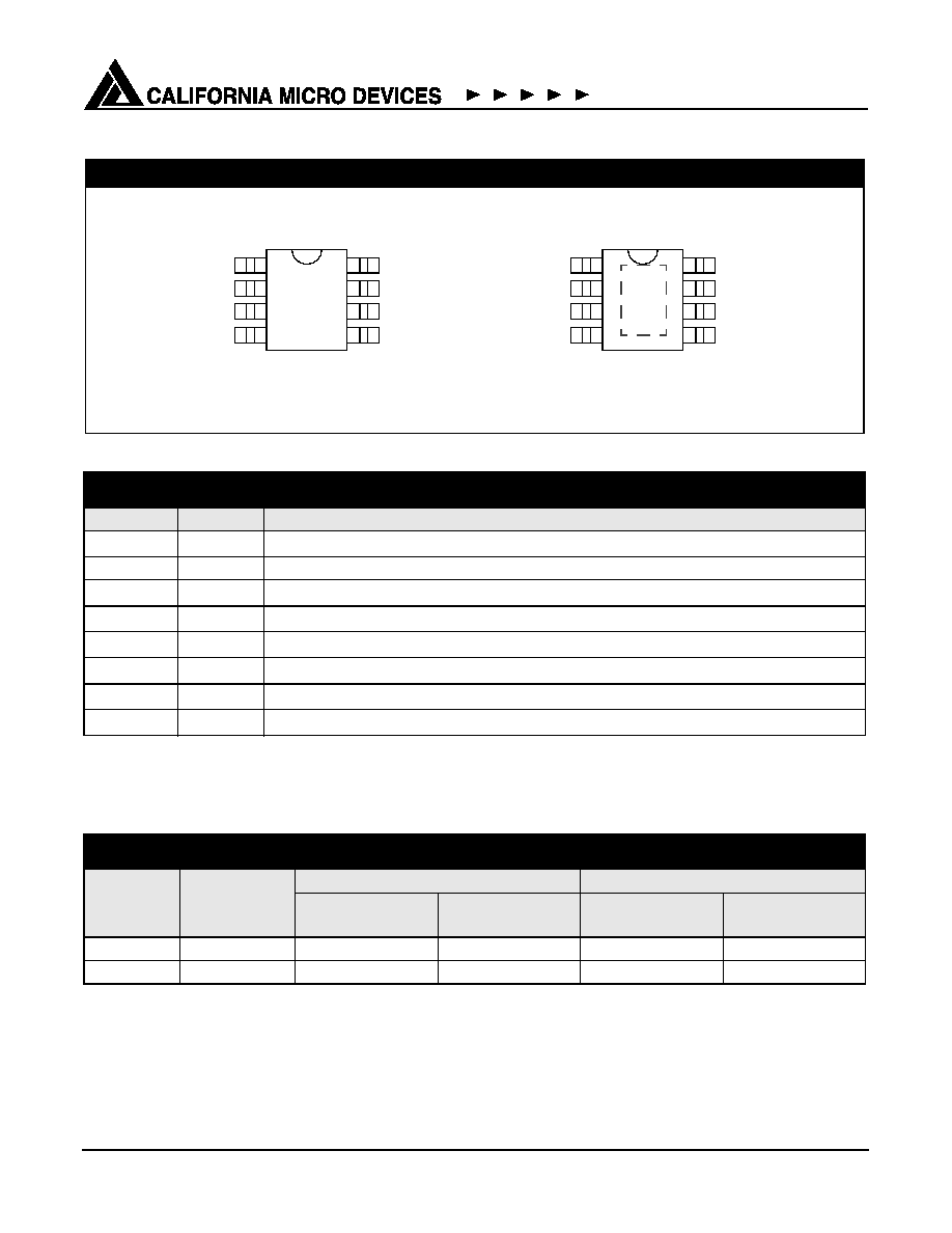
PACKAGE / PINOUT DIAGRAM
Note: This drawing is not to scale.
8-lead SOIC
1
2
3
4
8
7
6
5
NC
GND
V
SENSE
V
REF
V
TT
PV
IN
AV
IN
V
DDQ
T
OP VIEW
8-lead PSOP
TOP VIEW
1
2
3
4
8
7
6
5
NC
GND
V
SENSE
V
REF
V
TT
PV
IN
AV
IN
V
DDQ
GND
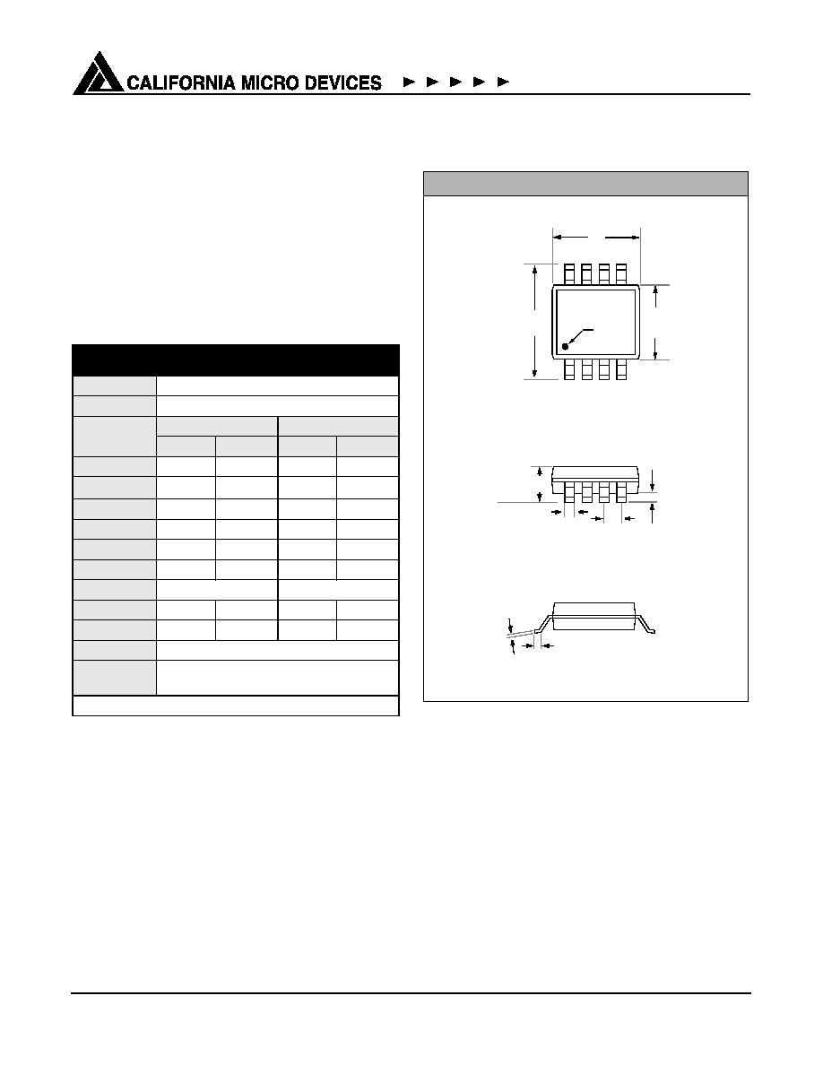
PART NUMBERING INFORMATION
Pins
Package
Standard Finish
Lead-free Finish
Ordering Part
Number
1
Part Marking
Ordering Part
Number
1
Part Marking
8
SOIC-8
CM3106-12SN
CM310601S
CM3106-12SM
CM3106-12SM
8
PSOP-8
CM3106-12SB
CM3106-12SB
CM3106-12SH
CM3106-12SH
© 2004 California Micro Devices Corp. All rights reserved.
02/02/04
430 N. McCarthy Blvd., Milpitas, CA 95035-5112
L Tel: 408.263.3214 L Fax: 408.263.7846 L www.calmicro.com
3
CM3106
Specifications
Note 1: These devices must be derated based on thermal resistance at elevated temperatures. The device packaged in a 8-lead
SOIC leadframe must be derated at
JA
= 151
∞C/W
.
JA
of the 8-lead PSOP is 40
∞C/W.
Note 1: Operating Characteristics are over Standard Operating Conditions unless otherwise specified.
ABSOLUTE MAXIMUM RATINGS
PARAMETER
RATING
UNITS
AV
IN
Operating Supply Voltage
7
V
V
DDQ
Input Voltage
7
V
Pin Voltages
V
TT
Output
Any other pins
7
7
V
V
ESD (HBM)
±2000
V
Storage Temperature Range
-40 to +150
∞C
Operating Temperature Range
Ambient
Junction
-40 to +85 (see note1)
-40 to +150
∞C
∞C
Power Dissipation (see note 1)
Internally Limited
W
STANDARD OPERATING CONDITIONS
PARAMETER
VALUE
UNITS
V
DDQ
2.5
V
AV
IN
2.5
V
PV
IN
2.5
V
Ambient Operating Temperature
0 to +70
∞C
C
TT
220 +20%
µF
ELECTRICAL OPERATING CHARACTERISTICS
(SEE NOTE 1)
SYMBOL
PARAMETER
CONDITIONS
MIN
TYP
MAX
UNITS
V
IN
Input Voltage Range
V
DDQ
AV
IN
2.2
2.2
2.5
2.5
AV
IN
5.5
V
V
I
CC
AV
IN
Quiescent Current
I
VTT
= 0A
450
µA
V
RLOAD
Load Regulation
0A < I
VTT
< 2.0A or -2.0A < I
VTT
< 0A
6.25
mV
V
REF
Output Reference Voltage
V
DDQ
=2.5V, I
REF
=0A
1.225
1.25
1.275
V
VOS
VTT
Output Offset from V
REF
-20
20
mV
Z
REF
V
REF
Output Impedance
-5
µA < I
REF
< 5
µA
5
k
Z
VDDQ
V
DDQ
Input Impedance
100
k
I
LIM
V
TT
Current Limit
2.5
A
T
DISABLE
T
HYST
Shutdown Temperature
Thermal Hysteresis
150
50
∞C
∞C
© 2004 California Micro Devices Corp. All rights reserved.
4
430 N. McCarthy Blvd., Milpitas, CA 95035-5112
L Tel: 408.263.3214 L Fax: 408.263.7846 L www.calmicro.com
02/02/04
CM3106
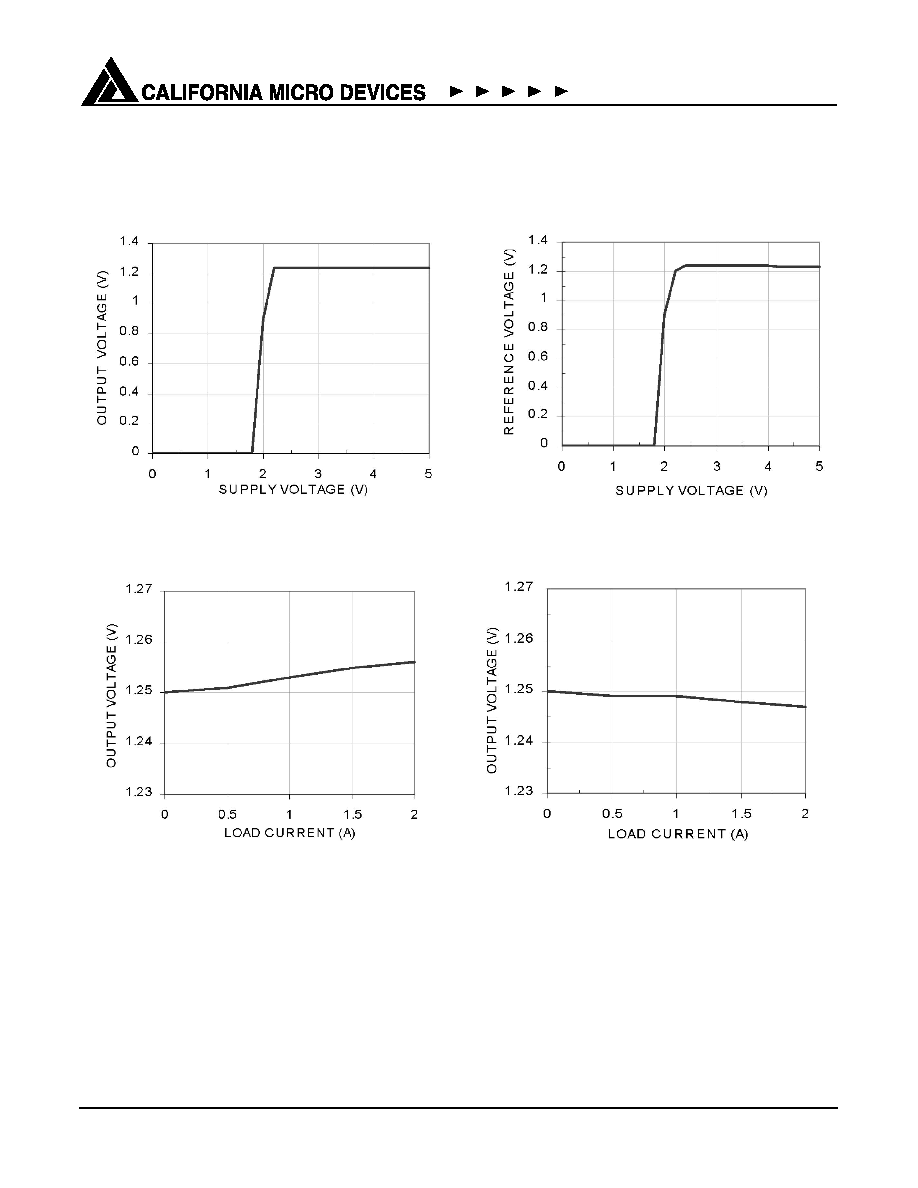
Performance Information
Typical DC Characteristics (nominal conditions unless otherwise specified)
Figure 1. Output Voltage with
AV
IN
Supply (V
DDQ
=2.5V)
Figure 2. Load Regulation (Sink)
Figure 3. Reference Voltage with
AV
IN
Supply (V
DDQ
=2.5V)
Figure 4. Load Regulation (Source)

© 2004 California Micro Devices Corp. All rights reserved.
02/02/04
430 N. McCarthy Blvd., Milpitas, CA 95035-5112
L Tel: 408.263.3214 L Fax: 408.263.7846 L www.calmicro.com
5
CM3106
Performance Information (cont'd)
Typical DC Characteristics (nominal conditions unless otherwise specified)
Figure 5. Over Current Limit (Sink)
Figure 6. AV
IN
Supply Current with Supply Voltage
Figure 7. Over Current Limit (Source)
© 2004 California Micro Devices Corp. All rights reserved.
6
430 N. McCarthy Blvd., Milpitas, CA 95035-5112
L Tel: 408.263.3214 L Fax: 408.263.7846 L www.calmicro.com
02/02/04
CM3106
Performance Information (cont'd)
Typical Transient Characteristics (nominal conditions unless otherwise specified)
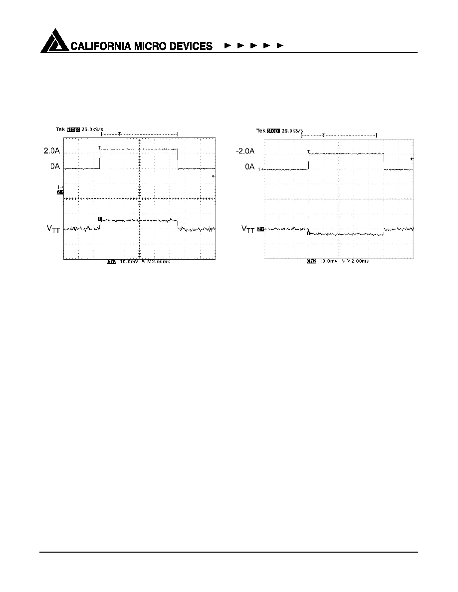
Figure 8. Load Transient
(0A to 2.0A Sink)
Figure 9. Line Transient
(0A to 2.0A Source)
© 2004 California Micro Devices Corp. All rights reserved.
02/02/04
430 N. McCarthy Blvd., Milpitas, CA 95035-5112
L Tel: 408.263.3214 L Fax: 408.263.7846 L www.calmicro.com
7
CM3106
Performance Information (cont'd)
Typical Thermal Characteristics (nominal conditions unless otherwise specified)
The overall junction to ambient thermal resistance
(
JA
) for device power dissipation (P
D
) consists prima-
rily of two paths in series. The first path is the junction
to the case (
JC
) which is defined by the package style,
and the second path is case to ambient (
CA
) thermal
resistance which is dependent on board layout. The
final operating junction temperature for any set of con-
ditions can be estimated by the following thermal equa-
tion:
T
JUNC
= T
AMB
+ P
D
(
JC
) + P
D
(
CA
)
= T
AMB
+ P
D
(
JA
)
When a CM3106-12SN is mounted on a double sided
printed circuit board with two square inches of copper
allocated for "heat spreading", the resulting
JA
is
151∞C/W. Based on the over temperature limit of 150∞C
with an ambient of 70∞C, the available power of this
package will be:
P
D
= (150∞C - 85∞C) / 151∞C/W = 0.43W
Since the
JA
of the CM3106-12SB (PSOP) is 40∞C/W,
the available power for this package will be:
P
D
= (150∞C - 85∞C) / 40∞C/W = 1.625W
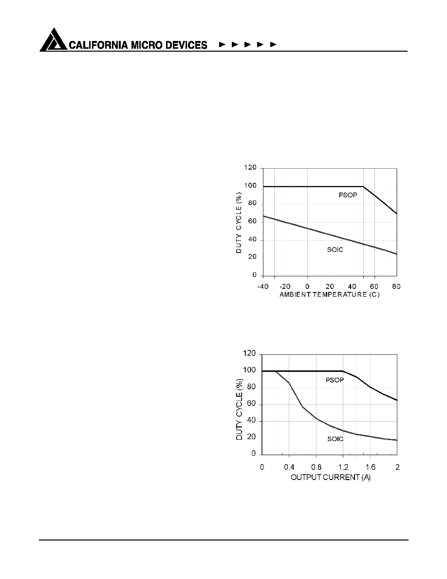
DDR Memory Application
Since the output voltage is 1.25V, and the device can
either source current from V
DD
or sink current to
Ground, the power dissipated in the device at any time
is 1.25V times the current load. This means the the
maximum average RMS current (in either direction) is
0.344A for the CM3106-12SN and 1.3A for the
CM3106-12SB. The maximum instantaneous current is
specified at 2A, so this condition should not be
exceeded for more than 17% of the time for the
CM3106-12SN and 65% of the time for the CM3106-
12SB. It is highly unlikely in most usage of DDR mem-
ory that this might occur, because it means the DDR
memory outputs are either all high or all low for 17%
(SOIC) and 65% (PSOP) of the time.
If the ambient temperature is 40∞C instead of 85∞C,
which is typically the maximum in most DDR memory
applications, the power dissipated (P
D
) can be 0.73W,
for the CM3106-12SN and 2.75W for the CM3106-
12SB. So the maximum average RMS current
increases from 0.42A to 0.58A for the CM3106-12SN
and a maximum instantaneous current of 2A should
not be exceeded for more than 29% of the time. For
CM3106-12SB, the maximum RMS current increases
from 1.3A to 2.2A. Thus, the maximum continuous cur-
rent can be 2A all the time.
Figure 10. Duty Cycle vs. Ambient
Temperature (I
LOAD
=2.0A)
Figure 11. Duty Cycle vs. Output
Current (Temp=70∞C)
© 2004 California Micro Devices Corp. All rights reserved.
8
430 N. McCarthy Blvd., Milpitas, CA 95035-5112
L Tel: 408.263.3214 L Fax: 408.263.7846 L www.calmicro.com
02/02/04
CM3106
Performance Information (cont'd)
Typical Thermal Characteristics (cont'd) (nominal conditions unless otherwise specified)
The theoretical calculations of these relationships
show the safe operating area of the CM3106 in the
SOIC package.
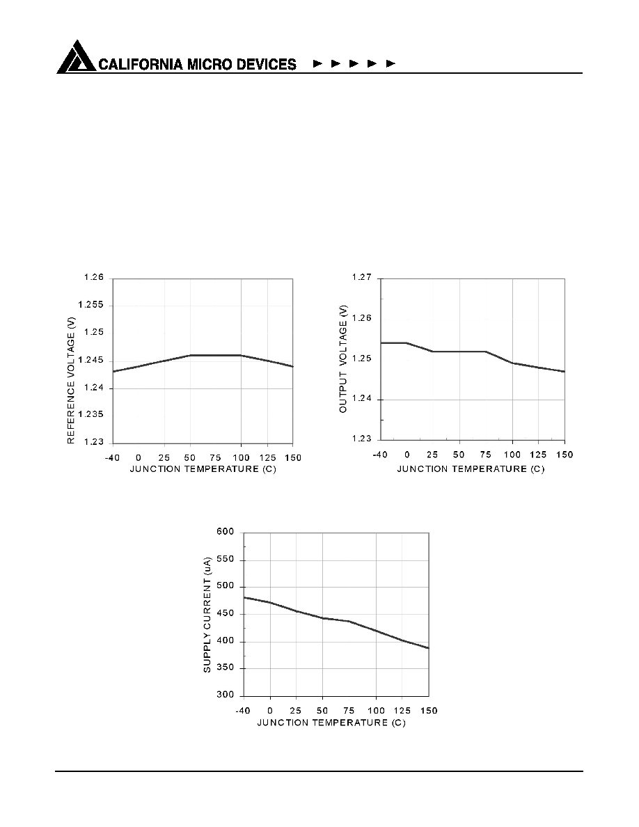
Thermal characteristics were measured using a double
sided board with two square inches of copper area
connected to the GND pins for "heat spreading".
Measurements showing performance up to a junction
temperature of 150∞C were performed under light load
conditions (5mA). This allows the ambient temperature
to be representative of the internal junction tempera-
ture.
Note: The use of multi-layer board construction with
separate ground and power planes will further enhance
the overall thermal performance.
Figure 12. Reference Voltage vs. Temperature
Figure 13. V
TT
Output Voltage vs.Temperature
(5mA load)
Figure 14. AV
IN
Quiescent Current vs.Temperature

© 2004 California Micro Devices Corp. All rights reserved.
02/02/04
430 N. McCarthy Blvd., Milpitas, CA 95035-5112
L Tel: 408.263.3214 L Fax: 408.263.7846 L www.calmicro.com
9
CM3106
Application Information
Figure 15. Typical Application Circuit
PCB Layout Considerations
The CM3106-12SB has a heat spreader attached to
the underneath of the PSOP-8 package in order for
heat to be transferred much easier from the package to
the PCB. The heat spreader is a copper pad of dimen-
sions just smaller than the package itself. By position-
ing the matching pad on the PCB top layer to connect
to the spreader during manufacturing, the heat will be
transferred between the two pads. The drawing below
shows the recommended PCB layout. Note that there
are six vias on either side to allow the heat to dissipate
into the ground and power planes on the inner layers of
the PCB. Vias can be placed underneath the chip, but
this can cause blockage of the solder. The ground and
power planes should be at least 2 sq in. of copper by
the vias. It also helps dissipation to spread if the chip is
positioned away from the edge of the PCB, and not
near other heat dissipating devices. A good thermal
link from the PCB pad to the rest of the PCB will ensure
a thermal link from the CM3106 package to ambient,
JA
, of around 40∞C/W.
Figure 16. Recommended Heat Sink PCB Layout
C
PVIN
47
µF
PV
IN
AV
IN
C
AVIN
47
µF
V
DDQ
AV
IN
PV
IN
GND
V
TT
C
TT
220
µF
V
TT
V
SENSE
V
REF
V
DDQ
V
REF
C
REF
0.1
µF
CM3106
© 2004 California Micro Devices Corp. All rights reserved.
10
430 N. McCarthy Blvd., Milpitas, CA 95035-5112
L Tel: 408.263.3214 L Fax: 408.263.7846 L www.calmicro.com
02/02/04
CM3106
Mechanical Details
The CM3106 is available in an 8-lead SOIC and PSOP
package.
SOIC-8 Mechanical Specifications
Dimensions for CM3106 devices packaged in 8-pin
SOIC packages are presented below.
For complete information on the SOIC-8 package, see
the California Micro Devices SOIC Package Informa-
tion document.
* This is an approximate number which may vary.
Package Dimensions for SOIC-8
PACKAGE DIMENSIONS
Package
SOIC
Leads
8
Dimensions
Millimeters
Inches
Min
Max
Min
Max
A
1.35
1.75
0.053
0.069
A
1
0.10
0.25
0.004
0.010
B
0.33
0.51
0.013
0.020
C
0.19
0.25
0.007
0.010
D
4.80
5.00
0.189
0.197
E
3.80
4.19
0.150
0.165
e
1.27 BSC
0.050 BSC
H
5.80
6.20
0.228
0.244
L
0.40
1.27
0.016
0.050
# per tube
100 pieces*
# per tape
and reel
2500 pieces
Controlling dimension: inches
Mechanical Package Diagrams
E
D
H
TOP VIEW
L
END VIEW
C
e
B
A
A
1
SEATING
PLANE
SIDE VIEW
1
2
3
4
8
7
6
5
Pin 1
Marking
© 2004 California Micro Devices Corp. All rights reserved.
02/02/04
430 N. McCarthy Blvd., Milpitas, CA 95035-5112
L Tel: 408.263.3214 L Fax: 408.263.7846 L www.calmicro.com
11
CM3106
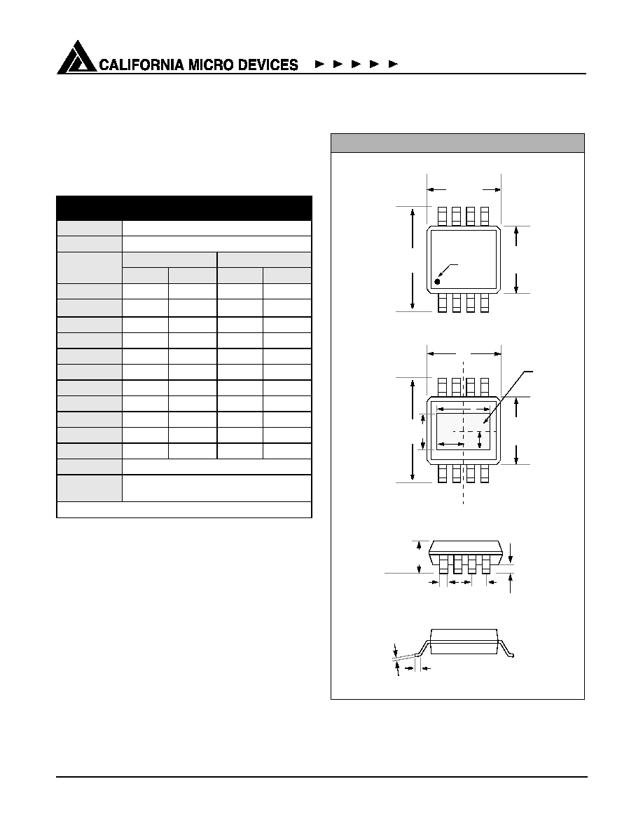
Mechanical Details
PSOP-8 Mechanical Specifications
Dimensions for CM3106 devices packaged in 8-pin
PSOP packages with an intagrated heatslug are pre-
sented below.
* This is an approximate number which may vary.
**
Centered on package centerline.
Package Dimensions for PSOP-8
PACKAGE DIMENSIONS
Package
PSOP-8
Leads
8
Dimensions
Millimeters
Inches
Min
Max
Min
Max
A
1.30
1.62
0.051
0.064
A
1
0.03
0.10
0.001
0.004
B
0.33
0.51
0.013
0.020
C
0.18
0.25
0.007
0.010
D
4.83
5.00
0.190
0.197
E
3.81
3.99
0.150
0.157
e
1.02
1.52
0.040 0.060
H
5.79
6.20
0.228
0.244
L
0.41
1.27
0.016
0.050
x**
3.30
3.81
0.130
0.150
y**
2.29
2.79
0.090
0.110
# per tube
100 pieces*
# per tape
and reel
2500 pieces
Controlling dimension: inches
Mechanical Package Diagrams
H
TOP VIEW
L
END VIEW
C
e
B
A
A1
SEATING
PLANE
SIDE VIEW
1
2
3
4
8
7
6
5
Pin 1
E
D
H
BOTTOM VIEW
1
2
3
4
8
7
6
5
x
y
y/2
x/2
Marking
D
E
Heat Slug