© 2004 California Micro Devices Corp. All rights reserved.
02/02/04
430 N. McCarthy Blvd., Milpitas, CA 95035-5112
L Tel: 408.263.3214
L Fax: 408.263.7846 L www.calmicro.com
1
CM3107
2 Amp Source/ Sink Bus Termination Regulator
for DDR Memory and Front Side Bus Applications
Features
∑
Ideal for Intel 865 Front Side Bus V
TT
and DDR
V
TT
applications
∑
Sinks and sources 2 Amps
∑
Over current protection
∑
Over temperature protection
∑
Integrated power MOSFETs
∑
Excellent accuracy (0.5% load regulation)
∑
Selectable output (1.225V/1.45V or V
DDQ
/2)
∑
8-lead SOIC and PSOP packages
∑
Lead-free versions available
Applications
∑
Intel 865/845 Front Side Bus termination
∑
Single and dual DDR memory termination
∑
Active termination buses
∑
Graphics card DDR memory termination
Product Description
The CM3107 is a sinking and sourcing regulator specif-
ically designed for series-parallel bus termination for
high-speed chip set busses as well as DDR memory
systems. It can source and sink current up to 2.0A with
a load regulation of 0.5%. The V
TT
output voltage is
selectable by V
DDQ
SEL and FSBSEL pins. The
V
DDQ
SEL pin controls whether the CM3107 is in DDR
memory mode with V
TT
=V
DDQ
/2, or in FSB mode. In
FSB mode, FSBSEL controls whether V
TT
is 1.225V or
1.45V. This allows the same chip to be used in two dif-
ferent circuits on an Intel 865-based motherboard.
The CM3107 provides over current and over tempera-
ture protection, which protect the chip from excessive
heating due to high current and high temperature. A
shutdown capability using an external transistor
reduces power consumption and provides a high
impedance output.
The CM3107 is housed in 8-lead SOIC and PSOP
packages and is available with optional lead-free finish-
ing.
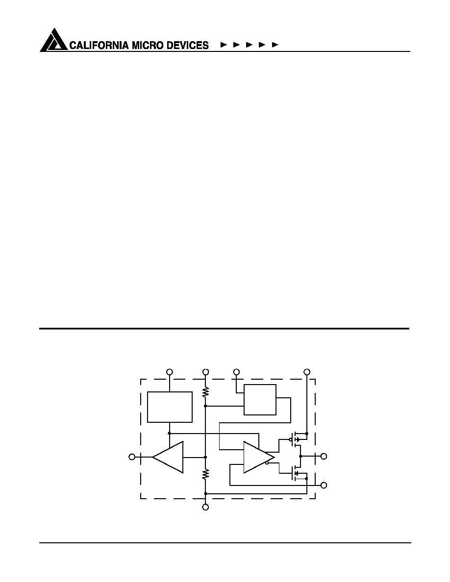
Simplified Electrical Schematic
V
REF
V
CC
GND
Over Current
V
SENSE
50
K
Over Temp
Reference
IN
OUT
Buffer
Output
Select
V
TT
Driver
50
K
V
DDQ
SEL FSBSEL
V
DDQ

© 2004 California Micro Devices Corp. All rights reserved.
2
430 N. McCarthy Blvd., Milpitas, CA 95035-5112
L Tel: 408.263.3214
L Fax: 408.263.7846 L www.calmicro.com
02/02/04
CM3107
Note 1: Assumes V
DDQ
and V
DDQ
SEL are tied together in DDR application.
Ordering Information
Note 1: Parts are shipped in Tape & Reel form unless otherwise specified.
PIN DESCRIPTIONS
SOIC-8
NAME
DESCRIPTION
LEAD(S)
1
V
DDQ
V
DDQ
2
V
TT
Outputs either 1.225V/1.45V FSB or V
DDQ
/2 DDR (See note 1)
3
GND
Ground
4
V
SENSE
Feedback voltage input
5
FSBSEL
Selects FSB output for
either V
TT
=1.225V or 1.45V
6
V
REF
1.25V reference voltage input for DDR bus
7
V
DDQ
SEL
Select output to support FSB or DDR applications
8
V
CC
Power for internal control circuits
PACKAGE / PINOUT DIAGRAM
Note: This drawing is not to scale.
8-lead SOIC
1
2
3
4
8
7
6
5
V
DDQ
V
TT
GND
V
SENSE
V
CC
V
DDQ
SEL
V
REF
FSBSEL
TOP VIEW
8-lead PSOP
1
2
3
4
8
7
6
5
V
DDQ
V
TT
GND
V
SENSE
V
CC
V
DDQ
SEL
V
REF
FSBSEL
TOP VIEW
GND
PART NUMBERING INFORMATION
Pins
Package
Standard Finish
Lead-free Finish
Ordering Part
Number
1
Part Marking
Ordering Part
Number
1
Part Marking
8
PSOP-8
CM3107-00SB
CM3107-00SB
CM3107-12SH
CM3107-00SH
8
SOIC-8
CM3107-00SN
CM310701S
CM3107-00SM
CM3107-00SM

© 2004 California Micro Devices Corp. All rights reserved.
02/02/04
430 N. McCarthy Blvd., Milpitas, CA 95035-5112
L Tel: 408.263.3214
L Fax: 408.263.7846
L www.calmicro.com
3
CM3107
Specifications
Note 1: These devices must be derated based on thermal resistance at elevated temperatures. The device packaged in a 8-lead
SOIC leadframe must be derated at
JA
= 151
∞C/W
.
JA
of the 8-lead PSOP is 40
∞C/W.
ABSOLUTE MAXIMUM RATINGS
PARAMETER
RATING
UNITS
V
CC
Operating Supply Voltage
7
V
V
DDQ
Input Voltage
7
V
Pin Voltages
V
TT
Output
Any other pins
7
7
V
V
ESD (HBM)
±2000
V
Storage Temperature Range
-40 to +150
∞C
Operating Temperature Range
Ambient
Junction
-40 to +85
-40 to +150
∞C
∞C
Power Dissipation (see note 1)
Internally Limited
W
STANDARD OPERATING CONDITIONS
PARAMETER
VALUE
UNITS
V
DDQ
2.5 to 3.3
V
V
CC
2.5 to 3.3
V
Ambient Operating Temperature
0 to +70
∞C
CV
OUT
220
±20%
µF

© 2004 California Micro Devices Corp. All rights reserved.
4
430 N. McCarthy Blvd., Milpitas, CA 95035-5112
L Tel: 408.263.3214
L Fax: 408.263.7846 L www.calmicro.com
02/02/04
CM3107
Specifications (cont'd)
Note 1: Operating Characteristics are over Standard Operating Conditions unless otherwise specified.
ELECTRICAL OPERATING CHARACTERISTICS
(SEE NOTE 1)
SYMBOL
PARAMETER
CONDITIONS
MIN
TYP
MAX
UNITS
V
IN
Input Voltage Range
V
DDQ
V
CC
2.2
2.2
2.5
2.5
V
CC
5.5
V
V
I
CC
V
CC
Quiescent Current
I
VTT
= 0A
450
µA
V
TT
Output Voltage
I
VTT
= 0A, V
DDQ
= 2.5V,
V
DDQ
SEL= logic "1" = 2.5V
V
DDQ
SEL= logic "0", FSBSEL= logic "0"
V
DDQ
SEL = logic "0", FSBSEL = logic "1"
I
VTT
= 0A, V
DDQ
= 3.3V,
V
DDQ
SEL= logic "0", FSBSEL= logic "0"
V
DDQ
SEL = logic "0", FSBSEL = logic "1"
1.225
1.200
1.425
1.200
1.425
1.250
1.225
1.450
1.225
1.450
1.275
1.250
1.475
1.250
1.475
V
V
V
V
V
V
V
RLOAD
Load Regulation
0A < I
VTT
< 2.0A or 0A < I
VTT
< -2.0A
6.25
mV
V
REF
Output Reference Voltage
V
DDQ
SEL = 2.5V, I
VREF
=0A
1.225
1.250
1.275
V
VOS
VTT
Output Offset from V
REF
-20
20
mV
Z
REF
V
REF
Output Impedance
-5
µA < I
VREF
< 5
µA
5
k
Z
VDDQSEL
V
VDDQSEL
Input Impedance
100
k
CL
VTT
V
TT
Current Limit
2.5
A
V
FSBSEL
Output Selection Logic
(FSBSEL)
Logic "1" Level
Logic "0" Level
1.5
0.4
V
V
T
DISABLE
T
HYST
Shutdown Temperature
Thermal Hysteresis
150
50
∞C
∞C

© 2004 California Micro Devices Corp. All rights reserved.
02/02/04
430 N. McCarthy Blvd., Milpitas, CA 95035-5112
L Tel: 408.263.3214
L Fax: 408.263.7846
L www.calmicro.com
5
CM3107
Performance Information
Typical DC Characteristics (nominal conditions unless otherwise specified)
Figure 1. Output Voltage with
V
CC
Supply (V
DDQ
SEL= 2.5V)
Figure 2. Load Regulation (Sink)
Figure 3. Reference Voltage with
V
CC
Supply (V
DDQ
SEL= 2.5V)
Figure 4. Load Regulation (Source)