 | –≠–ª–µ–∫—Ç—Ä–æ–Ω–Ω—ã–π –∫–æ–º–ø–æ–Ω–µ–Ω—Ç: CM3109 | –°–∫–∞—á–∞—Ç—å:  PDF PDF  ZIP ZIP |

©
2004 California Micro Devices Corp. All rights reserved.
01/15/04
430 N. McCarthy Blvd., Milpitas, CA 95035-5112
Tel: 408.263.3214
Fax: 408.263.7846
www.calmicro.com
1
CM3109
2A Sink/Source Regulator for Front Side Bus and
DDR Memory Bus Termination
Features
∑
Ideal for both PC Front Side Bus and DDR memory
V
TT
applications
∑
Sinks and sources 2A
∑
Over current protection
∑
Over temperature protection
∑
Shutdown function
∑
Integrated power MOSFETs
∑
Excellent accuracy (0.5% of load regulation)
∑
Minimum external components
∑
8 pin PSOP package
∑
Lead-free version available
Applications
∑
PC Front Side Bus termination regulator
∑
DDR Memory termination regulator
∑
Active termination buses
∑
Graphics card DDR memory termination
Product Description
The CM3109 is a sinking and sourcing regulator specif-
ically designed for series-parallel bus termination for
high speed chip set buses as well as DDR memory
systems. It can source and sink current up to 2A with
high accuracy of 0.5 %. The V
TT
output voltage is
selectable by V
DDQ
SEL and FSBSEL pins. The
V
DDQ
SEL pin controls whether the CM3109 is in DDR
memory mode with V
TT
= V
DDQ
/2, or in FSB mode. In
FSB mode, FSBSEL controls whether V
TT
is 1.225V or
1.45V. This allows the same chip to be used in two dif-
ferent circuits on PC motherboards that support both
Northwood and Prescott processors.
The CM3109 requires no external components to use
the GMCH Enable signal in Intel chipset or correspond-
ing signals for other chip sets when powering up the
PC. For the boards which support Suspend to RAM
(STR) functionality, CM3109 provides a shutdown (SD)
pin. When SD is set low, V
TT
will be in tri-state mode,
causing the output to go high impedance. In this mode,
CM3109 power is saved by significantly reducing the
quiescent current.
The CM3109 provides over current and over tempera-
ture protection. These features protect the chip from
excessive heating due to high current and high temper-
ature. The CM3109 is housed in an 8-pin PSOP pack-
age and is available with optional lead-free finishing.
Simplified Electrical
SD
V
CC
GND
Over Current
V
SENSE
50K
Over Temp
Reference
Output
Select
V
TT
Driver
50K
V
DDQ
SEL FSBSEL
V
DDQ
Schematic

©
2004 California Micro Devices Corp. All rights reserved.
2
430 N. McCarthy Blvd., Milpitas, CA 95035-5112
Tel: 408.263.3214
Fax: 408.263.7846
www.calmicro.com
01/15/04
CM3109
Note 1: Assumes V
DDQ
and V
DDQ
SEL are tied together in DDR application.
Ordering Information
Note 1: Parts are shipped in Tape & Reel form unless otherwise specified.
PIN DESCRIPTIONS
LEAD(S)
NAME
DESCRIPTION
1
V
DDQ
Input Voltage V
DDQ
2
V
TT
Outputs either 1.225V/1.45V FSB or V
DDQ
/2 DDR (See note 1)
3
SD
Shutdown input
4
V
SENSE
Feedback voltage input
5
FSBSEL
Select input for FSB output. Selects either V
TT
=1.225V or 1.45V.
6
GND
GROUND
7
V
DDQ
SEL
Select input for DDR/FSB Output
8
V
CC
Power for control blocks
PACKAGE / PINOUT DIAGRAM
Note: This drawing is not to scale.
8-lead PSOP
1
2
3
4
8
7
6
5
V
DDQ
V
TT
SD
V
SENSE
V
CC
V
DDQ
SEL
GND
FSBSEL
TOP VIEW
GND
PART NUMBERING INFORMATION
Leads
Package
Standard Finish
Lead-free Finish
Ordering Part
Number
1
Part Marking
Ordering Part
Number
1
Part Marking
8
PSOP-8
CM3109-00SB
CM3109-00SB
CM3109-00SH
CM3109-00SH

©
2004 California Micro Devices Corp. All rights reserved.
01/15/04
430 N. McCarthy Blvd., Milpitas, CA 95035-5112
Tel: 408.263.3214
Fax: 408.263.7846
www.calmicro.com
3
CM3109
Specifications
Note 1: These devices must be derated based on thermal resistance at elevated temperatures. The CM3109-xxSB/ must be der-
ated at
JA
= 40
∞C/W
. Please consult with factory for thermal evaluation assistance.
ABSOLUTE MAXIMUM RATINGS
PARAMETER
RATING
UNITS
V
CC
Operating Supply Voltage
7
V
V
DDQ
Input Voltage
7
V
Pin Voltages
V
TT
Output
Any other pins
7
7
V
V
Storage Temperature Range
-40 to +150
∞C
Operating Temperature Range
Ambient
Junction
-45 to +85
-45 to +150
∞C
∞C
Power Dissipation (See note 1)
Internally Limited
W
STANDARD OPERATING CONDITIONS
PARAMETER
VALUE
UNITS
V
DDQ
, V
DDQ
2.5
V
Ambient Operating Temperature
25
∞C
C
OUT
220
±20%
F

©
2004 California Micro Devices Corp. All rights reserved.
4
430 N. McCarthy Blvd., Milpitas, CA 95035-5112
Tel: 408.263.3214
Fax: 408.263.7846
www.calmicro.com
01/15/04
CM3109
Specifications (cont'd)
Note 1: Operating Characteristics are over Standard Operating Conditions unless otherwise specified.
ELECTRICAL OPERATING CHARACTERISTICS
(SEE NOTE 1)
SYMBOL
PARAMETER
CONDITIONS
MIN
TYP
MAX
UNITS
V
IN
Input Voltage Range
V
DDQ
V
CC
2.2
2.2
2.5
2.5
V
CC
5.5
V
V
I
CC
V
CC
Quiescent Current
I
VTT
= 0A
450
A
V
TT
Output Voltage
I
VTT
= 0A, V
DDQ
= 2.5V,
V
DDQ
SEL= "1" = 2.5V
V
DDQ
SEL="0", FSBSEL="0"
V
DDQ
SEL = "0", FSBSEL = "1"
I
VTT
= 0A, V
DDQ
= 3.3V,
V
DDQ
SEL="0", FSBSEL="0"
V
DDQ
SEL = "0", FSBSEL = "1"
1.225
1.200
1.425
1.200
1.425
1.250
1.225
1.450
1.225
1.450
1.275
1.250
1.475
1.250
1.475
V
V
V
V
V
V
V
RLOAD
Load Regulation
0A < I
VTT
< 2.0A or 0A < I
VTT
< -2.0A
6.25
mV
CL
VTT
V
TT
Current Limit
2.5
A
V
FSBSEL
Output Selection Logic (FSBSEL)
Logic "1" Level
Logic "0" Level
1.5
0.4
V
V
V
SD
Shutdown Logic
Logic "1" Level
Logic "0" Level
1.5
0.4
V
V
T
DISABLE
T
HYST
Shutdown Temperature
Thermal Hysteresis
150
30
∞C
∞C

©
2004 California Micro Devices Corp. All rights reserved.
01/15/04
430 N. McCarthy Blvd., Milpitas, CA 95035-5112
Tel: 408.263.3214
Fax: 408.263.7846
www.calmicro.com
5
CM3109
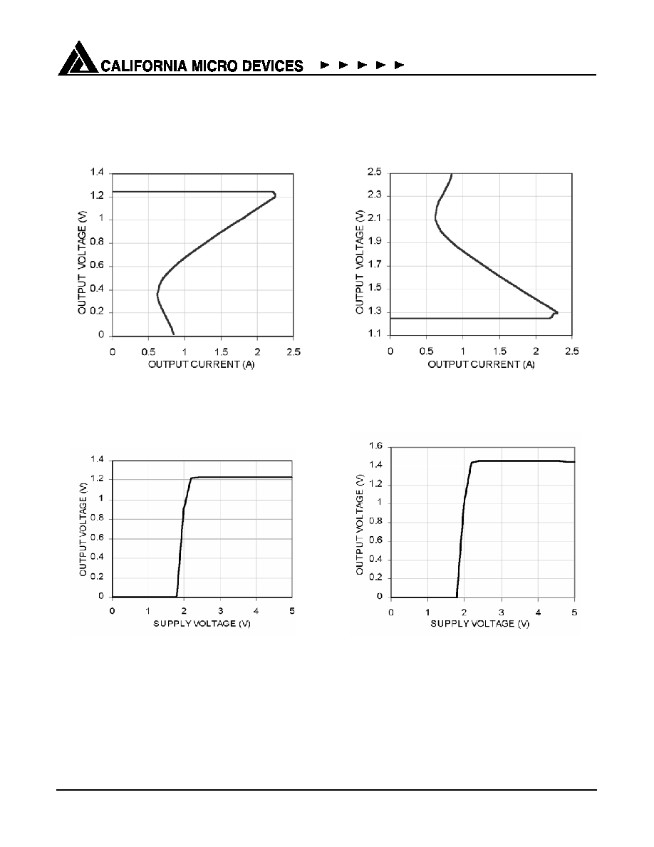
Performance Information
Typical DC Characteristics (nominal conditions unless otherwise specified)
Figure 1. Output Voltage with
V
CC
Supply (V
DDQ
=2.5V)
Figure 2. Load Regulation (Sink)
Figure 3. Reference Voltage with
V
CC
Supply (V
DDQ
=2.5V)
Figure 4. Load Regulation (Source)
©
2004 California Micro Devices Corp. All rights reserved.
6
430 N. McCarthy Blvd., Milpitas, CA 95035-5112
Tel: 408.263.3214
Fax: 408.263.7846
www.calmicro.com
01/15/04
CM3109
Performance Information (cont'd)
Typical DC Characteristics (nominal conditions unless otherwise specified)
Figure 5. Over Current Limit (Sink)
Figure 6. Output Voltage with V
CC
Supply Voltage
(V
DDQ
SEL = 0V, FSBSEL = 0V)
Figure 7. Over Current Limit (Source)
Figure 8. Output Voltage with V
CC
Supply Voltage
(V
DDQ
SEL = 0V, FSBSEL = 2.5V)

©
2004 California Micro Devices Corp. All rights reserved.
01/15/04
430 N. McCarthy Blvd., Milpitas, CA 95035-5112
Tel: 408.263.3214
Fax: 408.263.7846
www.calmicro.com
7
CM3109
Performance Information (cont'd)
Typical DC Characteristics (nominal conditions unless otherwise specified)
Figure 9. V
CC
Supply Current with
Supply Voltage
Typical Transient Characteristics (nominal conditions unless otherwise specified)
Figure 10. Load Transient
(0A to 1.5A Sink)
Figure 11. Line Transient
(0A to 1.5A Source)

©
2004 California Micro Devices Corp. All rights reserved.
8
430 N. McCarthy Blvd., Milpitas, CA 95035-5112
Tel: 408.263.3214
Fax: 408.263.7846
www.calmicro.com
01/15/04
CM3109
Performance Information (cont'd)
Typical Thermal Characteristics
The overall junction to ambient thermal resistance
(
JA
) for device power dissipation (P
D
) consists prima-
rily of two paths in series. The first path is the junction
to the case (
JC
) which is defined by the package style,
and the second path is case to ambient (
CA
) thermal
resistance which is dependent on board layout. The
final operating junction temperature for any set of con-
ditions can be estimated by the following thermal equa-
tion:
T
JUNC
= T
AMB
+ P
D
(
JC
) + P
D
(
CA
)
= T
AMB
+ P
D
(
JA
)
When a CM3109-00SB/SH (PSOP) is mounted on a
double sided printed circuit board with two square
inches of copper allocated for "heat spreading", the
resulting
JA
is 40∞C/W. Based on the over tempera-
ture limit of 150∞C with an ambient of 85∞C, the avail-
able power of this package will be:
P
D
= (150∞C -85∞C) / 40∞C/W = 1.625W
DDR Memory Application
Since the output voltage is 1.25V, and the device can
either source current from V
DDQ
or sink current to
Ground, the power dissipated in the device at any time
is 1.25V times the current load. This means the maxi-
mum average RMS current (in either direction) is 1.3A
for CM3109-00SB/SH. The maximum instantaneous
current is specified at 2A, so this condition should not
be exceeded 65% of the time. It is highly unlikely in
most usage of DDR memory that this might occur,
because it means the DDR memory outputs are either
all high or all low for 65% of the time.
If the ambient temperature is 40∞C instead of 85∞C,
which is typically the maximum in most DDR memory
applications, the power dissipated (P
D)
can be 2.75W.
So the maximum RMS current increases from 1.3A to
2.2A. Thus, the maximum continuous current can be
2A all the time.
Figure 12. Duty Cycle vs. Ambient
Temperature (I
LOAD
= 2A)
Figure 13. Duty Cycle vs. Output
Current (Temp=70∞C)
©
2004 California Micro Devices Corp. All rights reserved.
01/15/04
430 N. McCarthy Blvd., Milpitas, CA 95035-5112
Tel: 408.263.3214
Fax: 408.263.7846
www.calmicro.com
9
CM3109
Performance Information (cont'd)
Typical Thermal Characteristics (cont'd)
Front Side Bus Application
If the CM3109-00SB/SH is instead used for the Front
Side Bus application, where V
DDQ
could be connected
to the 3.3V V
CC
rail for ease of connectivity, the power
dissipated will increase to [3.3V-1.4V] = 1.9V times the
sourcing current, or [1.4V - 0V] = 1.4V times the sink-
ing current.
So the worst case is with all FSB outputs low for a
period of time, such that the maximum average source
current at an ambient of 40∞C is [2.75W / 1.9V] =
1.45A. If this average current is exceeded, the device
will go over-temperature and the output will drop to 0V.
The theoretical calculations of these relationships
show the safe operating area of the CM3109 in the
PSOP package.
Thermal characteristics were measured using a double
sided board with two square inches of copper area
connected to the GND pins for "heat spreading".
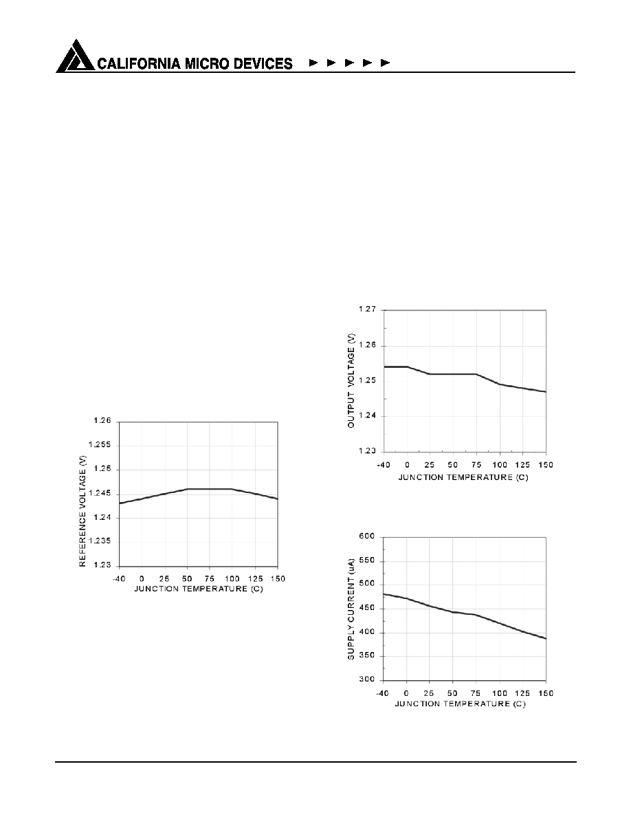
Figure 14. Reference Voltage vs. Temperature
Measurements showing performance up to a junction
temperature of 150∞C were performed under light load
conditions (5mA). This allows the ambient temperature
to be representative of the internal junction tempera-
ture.
Note: The use of multi-layer board construction with
separate ground and power planes will further enhance
the overall thermal performance.
Figure 15. Output Voltage vs. Ambient
Temperature (I
LOAD
=5mA)
Figure 16. Quiescent Current vs. Temperature

©
2004 California Micro Devices Corp. All rights reserved.
10
430 N. McCarthy Blvd., Milpitas, CA 95035-5112
Tel: 408.263.3214
Fax: 408.263.7846
www.calmicro.com
01/15/04
CM3109
Application Information
PCB Layout Considerations
The CM3109-00SB/SH has a heat spreader attached
to the underneath of the PSOP-8 package in order for
heat to be transferred much easier from the package to
the PCB. The heat spreader is a copper pad of dimen-
sions just smaller than the package itself. By position-
ing the matching pad on the PCB top layer to connect
to the spreader during manufacturing, the heat will be
transferred between the two pads. The drawing below
shows the recommended PCB layout. Note that there
are six vias on either side to allow the heat to dissipate
into the ground and power planes on the inner layers of
the PCB. Vias can be placed underneath the chip, but
this can cause blockage of the solder. The ground and
power planes should be at least 2 sq in. of copper by
the vias. It also helps dissipation to spread if the chip is
positioned away from the edge of the PCB, and not
near other heat dissipating devices. A good thermal
link from the PCB pad to the rest of the PCB will ensure
a thermal link from the CM3109 package to ambient,
JA
, of around 40∞C/W.
Figure 17. Recommended Heat Sink PCB Layout
©
2004 California Micro Devices Corp. All rights reserved.
01/15/04
430 N. McCarthy Blvd., Milpitas, CA 95035-5112
Tel: 408.263.3214
Fax: 408.263.7846
www.calmicro.com
11
CM3109
Application Information (cont'd)
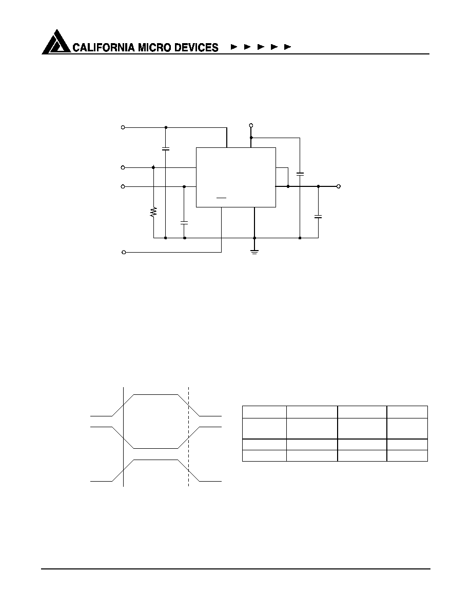
Figure 18. Typical Front Side Bus with Suspend to RAM Application Circuit
The above diagram shows the CM3109 connected to
the Intel 865 GMCH Front Side Bus V
TT
pin GMCH-
VCCP. The Enable signal GMCH_EN is used to shut
down the output of the CM3109 to save power during
shutdown periods. The V
DDQ
SEL input ensures that
the CM3109 is in Front Side Bus mode, and the BOOT-
SEL from the GMCH ensures the right Microprocessor
V
TT
voltage is applied.
Figure 19. Front Side Bus Timing diagram
Note 1:Assumes V
DDQ
and V
DDQ
SEL are tied
together in DDR application.
Table 1: V
TT
Output Selection Truth Table.
V
DDQ
BOOTSEL
V
DDQ
SEL
R
VDDQ
SEL
4.7K
FSBSEL
0.1uF
220uF
GMCHVCCP
V
CC
FSBSEL
V
DDQ
SEL
VDDQ
V
CC
V
TT
VSENSE
GND
CV
CC
47uF
CV
DDQ
47uF
CV
TT
GMCH_EN
SD
VCC (CPU Core)
GMCH_EN
GMCHVCCP
V
DDQ
SEL
FSBSEL
V
TT
NOTE
"1"
Don't Care
V
DDQ
SEL/2
(see note 1)
For DDR
Open or "0"
"0"
1.225V
For FSB
Open or "0"
"1"
1.45V
For FSB

©
2004 California Micro Devices Corp. All rights reserved.
12
430 N. McCarthy Blvd., Milpitas, CA 95035-5112
Tel: 408.263.3214
Fax: 408.263.7846
www.calmicro.com
01/15/04
CM3109
Mechanical Details
PSOP-8 Mechanical Specifications
Dimensions for CM3109 devices packaged in 8-pin
PSOP packages with an integrated heatslug are pre-
sented below.
For complete information on the PSOP-8 package, see
the California Micro Devices PSOP-8 Package Infor-
mation document.
* This is an approximate number which may vary.
**
Centered on package centerline.
Package Dimensions for PSOP-8
PACKAGE DIMENSIONS
Package
PSOP-8
Leads
8
Dimensions
Millimeters
Inches
Min
Max
Min
Max
A
1.30
1.62
0.051
0.064
A
1
0.03
0.10
0.001
0.004
B
0.33
0.51
0.013
0.020
C
0.18
0.25
0.007
0.010
D
4.83
5.00
0.190
0.197
E
3.81
3.99
0.150
0.157
e
1.02
1.52
0.040 0.050
H
5.79
6.20
0.228
0.244
L
0.41
1.27
0.016
0.050
x**
3.56
4.06
0.130
0.150
y**
2.29
2.79
0.090
0.110
# per tube
100 pieces*
# per tape
and reel
2500 pieces
Controlling dimension: inches
Mechanical Package Diagrams
H
TOP VIEW
L
END VIEW
C
e
B
A
A1
SEATING
PLANE
SIDE VIEW
1
2
3
4
8
7
6
5
Pin 1
E
D
H
BOTTOM VIEW
1
2
3
4
8
7
6
5
x
y
y/2
x/2
Marking
D
E
Heat Slug