 | –≠–ª–µ–∫—Ç—Ä–æ–Ω–Ω—ã–π –∫–æ–º–ø–æ–Ω–µ–Ω—Ç: CM3112 | –°–∫–∞—á–∞—Ç—å:  PDF PDF  ZIP ZIP |
© 2004 California Micro Devices Corp. All rights reserved.
01/20/04
430 N. McCarthy Blvd., Milpitas, CA 95035-5112
L Tel: 408.263.3214 L Fax: 408.263.7846 L www.calmicro.com
1
CM3112
PRELIMINARY
150mA/1.2V CMOS LDO Regulator
with Power Good
Features
∑
LDO regulator with Power Good
∑
No capacitor required on the LDO output
∑
Power Good (PG) control signal
∑
Regulated 1.2V output
∑
150mA output current
∑
Low quiescent operating current (90
µA typical)
∑
"Zero" disable mode current
∑
Foldback current limiting protection
∑
Thermal shutdown protection
∑
SOT23-5 package
∑
Micrel MIC5258, MIC5268 compatible pinout
∑
Lead-free version available
Applications
∑
Pentium
4 Motherboards
∑
PC Cards
∑
Peripheral Adapter Cards
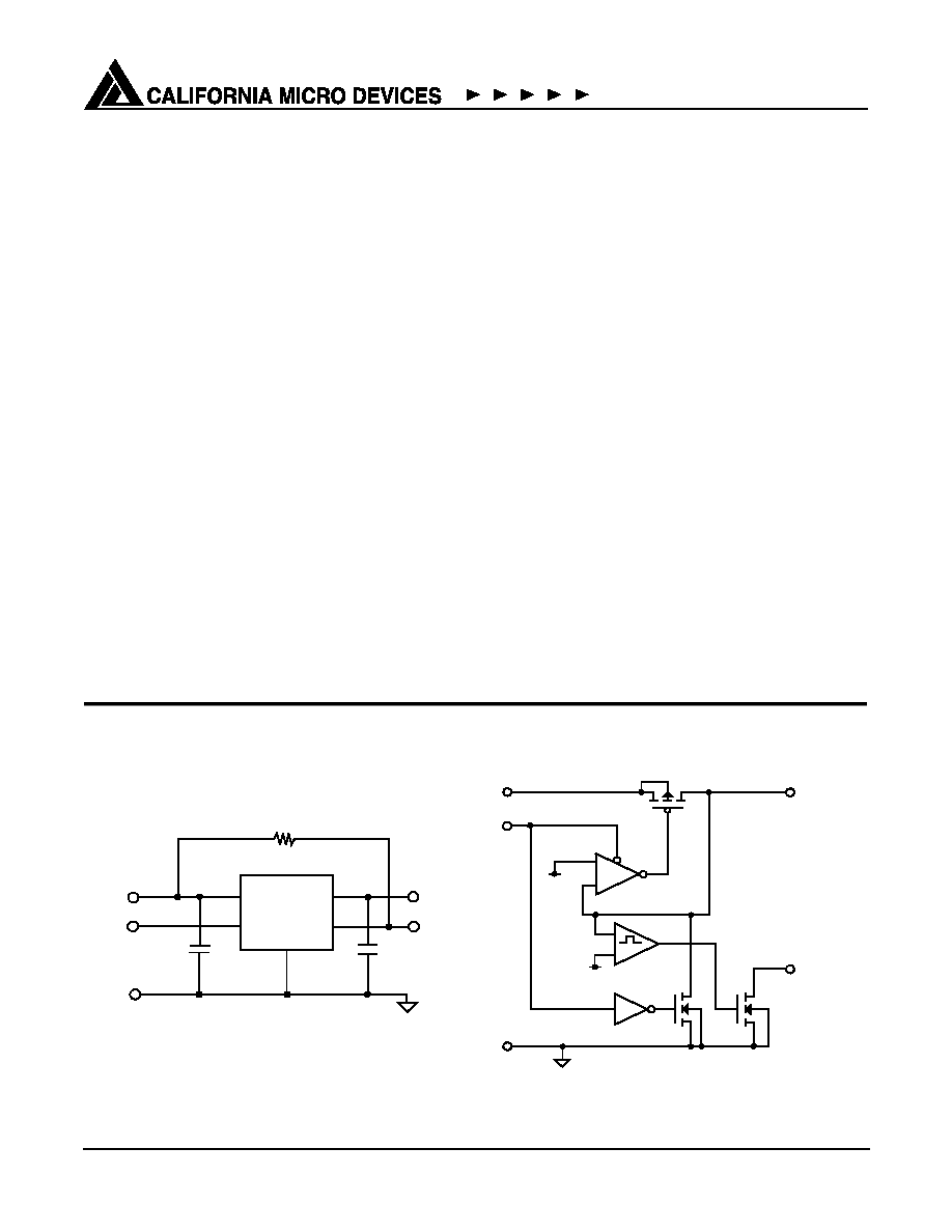
Product Description
The CM3112-12 is a low quiescent current (90uA) reg-
ulator that delivers up to 150mA of load current at a
fixed 1.2V output. All the necessary circuitry has been
included to deliver a 50
power good signal (open
drain) which remains for 5ms after the output has
exceeded 90% (typ) of its nominal level.
A dedicated control input (EN, Active High) has been
included for power-up sequencing flexibility. When this
input is taken low, the regulator is disabled. In this
state, the supply current will drop to near zero. An inter-
nal discharge MOSFET (500
) resistance will force the
output to ground whenever the device has been shut-
down.
The CM3112-12 is fully protected, offering both over-
load current limiting and high temperature thermal
shutdown.
Housed in a tiny SOT23 package, the device is ideal for
space critical applications and is also available with
optional lead-free finishing.
Simplified Electrical Schematic
Typical Application Circuit
IN
EN
OUT
GND
0.1
µ
F*
V
OUT
GND
CM3112-12
PG
1k
V
IN
PG
EN
* Optional
0.1
µ
F*
EN
+
IN
GND
OUT
-
V
REF
1.2V
2.5ms
+
-
V
REF
X 0.93
1X
PG
1.2V/150mA

© 2004 California Micro Devices Corp. All rights reserved.
2
430 N. McCarthy Blvd., Milpitas, CA 95035-5112
L Tel: 408.263.3214 L Fax: 408.263.7846 L www.calmicro.com
01/20/04
CM3112
PRELIMINARY
Ordering Information
Note 1: Parts are shipped in Tape & Reel form unless otherwise specified.
PIN DESCRIPTIONS
PIN
NAME
DESCRIPTION
1
IN
Positive input voltage for the regulator. The internal loading on this input is typically 300
µA when-
ever the regulator is enabled, and less than 10
µA when the regulator is disabled. If the IN pin is
within a few inches of the main input filter, a capacitor may not be necessary. Otherwise an input fil-
ter capacitor (C
IN
) of 0.1uF to 1uF will ensure adequate filtering.
2
GND
The negative reference for all voltages.
3
EN
Enable/shutdown input. When EN is asserted high (V
EN
1.6V), the regulator is enabled. When EN
is asserted low (V
EN
0.4V), the regulator's series pass transistor is forced into a high impedance
mode and an internal discharge resistance (500
) is applied to the output to quickly reduce the out-
put voltage to 0 volts.
4
PG
Power Good output. This is an open drain output and functions as a supply voltage supervisor for
the output voltage. It is asserted low when the output falls below 84% of its nominal value. This out-
put becomes inactive when (EN > 1.5V), (2.5V < V
IN
< 5.5V) and (V
OUT
> 97% of V
OUTNOM)
, all of
which are valid for more than 1-10ms.
5
OUT
The regulated voltage output. Although an output capacitor is not necessary for stable regulator
operation, a optional 0.1uF capacitor can be used to provide an added measure of output stability.
PACKAGE / PINOUT DIAGRAM
Note: This drawing is not to scale.
5-pin SOT23
IN
GND
EN
OUT
PG
1
2
5
3
4
F
A
12/
F
B
12
Top View
PART NUMBERING INFORMATION
Regulator
Pins
Package
Standard Finish
Lead-free Finish
Ordering Part
Number
1
Part Marking
Ordering Part
Number
1
Part Marking
CM3112-12
5
SOT23-5
CM3112-12ST
FA12
CM3112-12SO
FB12
© 2004 California Micro Devices Corp. All rights reserved.
01/20/04
430 N. McCarthy Blvd., Milpitas, CA 95035-5112
L Tel: 408.263.3214 L Fax: 408.263.7846 L www.calmicro.com
3
CM3112
PRELIMINARY
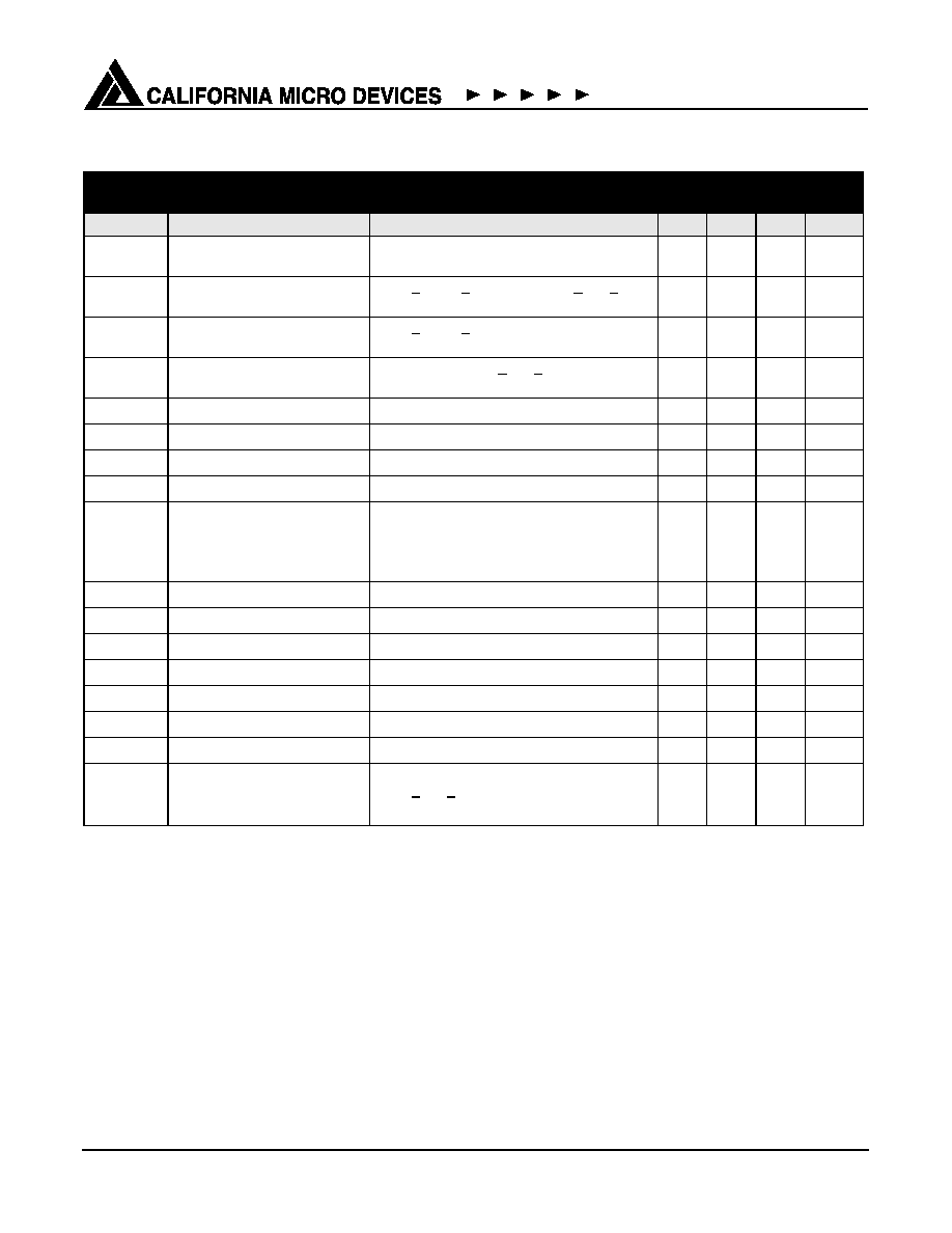
Specifications
Note 1: The power rating is based on a printed circuit board heat spreading capability equivalent to 2 square inches of copper con-
nected to the GND pins. Typical multi-layer boards using power plane construction will provide this heat spreading ability
without the need for additional dedicated copper area. Please consult with factory for thermal evaluation assistance.
ABSOLUTE MAXIMUM RATINGS
PARAMETER
RATING
UNITS
ESD Protection (HBM)
+2000
V
Pin Voltages
V
IN
V
OUT
V
EN
[GND - 0.6] to +6.0
[GND - 0.6] to [V
IN
+0.6]
[GND - 0.6] to [V
IN
+0.6]
V
V
V
Storage Temperature Range
-40 to +150
∞C
Operating Temperature Range
Ambient
Junction
0 to +70
0 to +150
∞C
∞C
Power Dissipation (See note 1)
Internally Limited
W
STANDARD OPERATING CONDITIONS
PARAMETER
VALUE
UNITS
V
IN
2.5 to 5.5
V
Ambient Operating Temperature Range
0 to +70
∞C
Load Current
0 to 150
mA
C
OUT
0 to 10
µF
© 2004 California Micro Devices Corp. All rights reserved.
4
430 N. McCarthy Blvd., Milpitas, CA 95035-5112
L Tel: 408.263.3214 L Fax: 408.263.7846 L www.calmicro.com
01/20/04
CM3112
PRELIMINARY
Note 1: Bold values indicate 0 ∞C < T
J
<125 ∞C.
ELECTRICAL OPERATING CHARACTERISTICS
(SEE NOTE 1)
SYMBOL
PARAMETER
CONDITIONS
MIN
TYP
MAX
UNITS
V
OUT
Output Voltage Accuracy
I
LOAD
= 5mA, V
IN
= 3.3V
-2
-3
2
3
%
%
V
OUT
Output Voltage
5mA < I
LOAD
< 150mA, 3.135V < V
IN
< 5.5V
-4
-5
4
5
%
%
V
R LOAD
Load Regulation
5mA < I
LOAD
< 100mA
0.5
0.7
%
%
V
R LINE
Line Regulation
xx
I
LOAD
= 5mA; 2.5V < V
IN
< 5.5V
0.1
0.15
%/V
%/V
R
DROP
Dropout Resistance
V
IN
= 2.7V
10
I
LIM
Overload Current Limit
160
400
mA
I
SC
Short Circuit Current Limit
V
OUT
< 0.5V
150
mA
R
DISCH
Discharge Resistance
EN tied to GND
500
I
GND
Ground Current
Regulator Enabled (EN=V
IN
); I
LOAD
= 0mA
Regulator Enabled (EN=V
IN
); I
LOAD
= 150mA
Regulator Disabled (EN=GND); (Disable
Mode)
90
100
0.01
150
200
10
µA
µA
µA
V
EN
EN Input Logic High Threshold
Regulator Enabled, V
IN
= 5.5V
1.6
V
V
DIS
EN Input Logic Low Threshold
Regulator Disabled, V
IN
= 5.5V
0.4
V
I
EN
Enable Input Current
0.01
10
µA
V
PGL
Power Good Low Threshold
% of V
OUT
(PG ON)
84
%
V
PGH
Power Good High Threshold
% of V
OUT
(PG OFF)
97
%
V
OL
Power Good Logic "0" Voltage
I
L
= 2mA; Fault Condition
0.05
0.1
V
I
PG
Power Good Leakage Current
Power Good Off; V
PG
= 5.5V
0.01
50
µA
D
PGD
D
PGA
Power Good Delay Time
To de-assert PG
To assert PG
2.5V < V
IN
< 5.5V (applies to D
PGD
only)
1
10
1
mS
mS
© 2004 California Micro Devices Corp. All rights reserved.
01/20/04
430 N. McCarthy Blvd., Milpitas, CA 95035-5112
L Tel: 408.263.3214 L Fax: 408.263.7846 L www.calmicro.com
5
CM3112
PRELIMINARY
Timing Diagram
Figure 1. Power Good Delay Timing
Active
Inactive
PG
EN
V
OUT
V
PG
D
PGA
D
PGD
100%
90%
D
PGD