
©
2004 California Micro Devices Corp. All rights reserved.
11/12/04
430 N. McCarthy Blvd., Milpitas, CA 95035-5112
Tel: 408.263.3214
Fax: 408.263.7846
www.calmicro.com
1
CM3121
PRELIMINARY
Dual Linear Voltage Regulator for DDR-I and DDR-II Memory
Features
∑
Fully integrated power solution for DDR memory
ICs
∑
Ideal for DDR-I (2.5V
DDQ
) and DDR-II (1.8V
DDQ
)
∑
Lowest system cost and smallest footprint with just
two external output capacitors
∑
Two linear regulators:
- V
DDQ
regulator with a maximum output current
of 1.5A shared by DRAM and V
TT
regulator
- source-sink V
TT
regulator with maximum out-
put current of 0.5A (DDR-I) or 0.3A (DDR-II)
∑
Fault output indicates overcurrent condition in
either regulator, under voltage lock-out and over-
temperature condition
∑
Reverse current protection if host is powered off
∑
PSOP-8 package with integrated heat spreader
∑
Lead-free versions available
Applications
∑
DDR-I and DDR-II memory power for:
-
Set Top Boxes, DVD Players, Games
-
Digital TVs, Flat Panel Displays
-
Printers, Digital Projectors
-
Embedded systems
-
Communications systems
Product Description
The CM3121 provides an integrated power solution for
DDR-I and DDR-II memory systems in consumer electron-
ics applications. The CM3121 is ideal for a 2.8V to 3.6V
supply for DDR-I memory and 2.2V to 2.8V for DDR-II mem-
ory. The CM3121 features two independent linear regula-
tors for V
DDQ
and V
TT
supply regulation. The default
voltage for V
DDQ
is 2.5V. The V
DDQ
regulator SENSE pin
allows for setting V
DDQ
in the 2.2V to 2.8V range, or DDR-II
memories from 1.7V to 1.9V. The V
TT
regulator output is
always half the V
DDQ
voltage, derived internally. A capacitor
should be connected to each of the two outputs.
When EN_DDR is set high, the two DDR regulators are dis-
abled to minimize overall system power dissipation such as
when memory is in standby.
The FAULT pin goes low whenever either of the two regula-
tors goes into current limit mode, the input voltage drops too
far or if overtemp occurs.
The CM3121 is available in a PSOP-8 package that has
excellent thermal dissipation. It is available with optional
lead-free finishing.
.
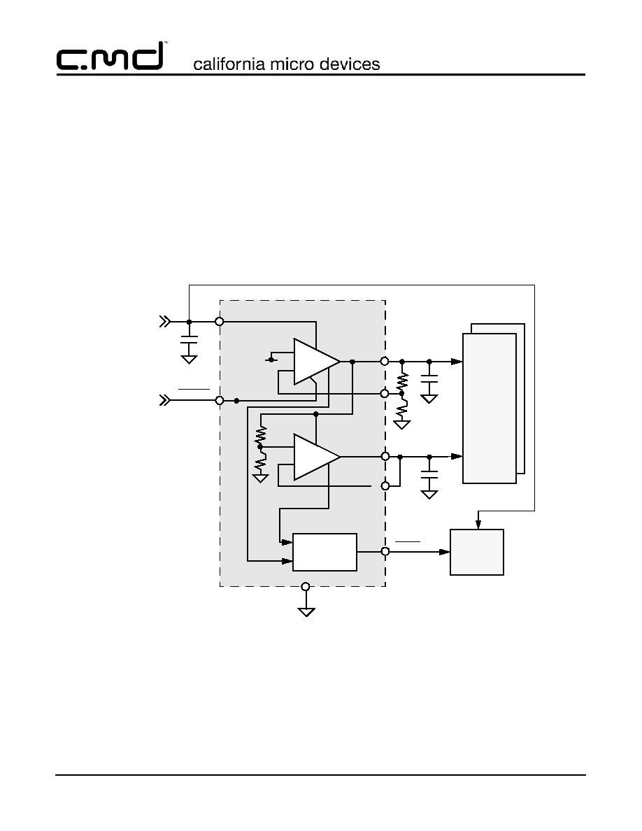
Typical Application Circuit
Circuit Schematic
V
REF
R
R
FAULT
V
TT
=1.25V
V
DDQ
= 2.5V
V
DDQ
REGULATOR
V
TT
REGULATOR
EN_DDR
V
CC
GND
C
DDQ
DDR
MEMORY
CPU
CORE
+ I/O
C
CC
C
TT
Enable DDR
Memory #
2.8V to 3.3V
SENSE V
TT
V
TT
SENSE V
TT
V
DDQ
SENSE
V
DDQ
CURRENT LIMIT
OVERTEMP
LOW INPUT
V
REF
R
R
FAULT
V
DDQ
REGULATOR
V
TT
REGULATOR
GND
SENSE V
TT
V
TT
SENSE V
TT
V
DDQ
SENSE
V
DDQ
CURRENT LIMIT
OVERTEMP
LOW INPUT
SENSE_V
TT
VTT
SENSE_ V
DDQ
V
DDQ
V
CC
EN_DDR
©
2004 California Micro Devices Corp. All rights reserved.
2
430 N. McCarthy Blvd., Milpitas, CA 95035-5112
Tel: 408.263.3214
Fax: 408.263.7846
www.calmicro.com
11/12/04
CM3121
PRELIMINARY
Functional Description
The CM3121 provides power for DDR-I/DDR-II memo-
ries from two voltage regulators on-chip. There is an
over-temperature thermal shutdown if any of the regu-
lators overheat. Each regulator also has reverse cur-
rent protection in the event of any being shut down.
The V
DDQ
linear regulator can provide 2.5V/1.8V for
DDR-I/-II memory at up to 1.5A. An external feedback
resistor divider R1 and R2, when connected to the
SENSE_V
DDQ
pin, enables selection of V
DDQ
output
voltages from 2.2V to 2.8V for use with DDR-I memo-
ries requiring other than 2.5V for V
DDQ
(see
Figure 5
).
In this mode, the voltage on VDDQ is detemined as fol-
lows:
V
DDQ
= 1.25V x
When SENSE_V
DDQ
is connected to GND or left open,
V
DDQ
is fixed at 2.50V (and V
TT
at 1.25V). For DDR-II
operation, V
DDQ
can be set from 1.7V to 1.9V. The V
TT
regulator is a linear source-sink regulator powered
from the V
DDQ
output that supplies the V
TT
supply
required by DDR-I memory termination resistors. This
regulator sinks or sources up to 0.5A. The V
TT
output
voltage accurately tracks V
DDQ
/2 to 1%. When there is
no V
CC
provided, V
TT
is powered down and its output
is 0V. This regulator has overload current limiting of
0.6A minimum.
The EN_DDR pin when set active low enables the
CM3121 to operate in normal mode with V
DDQ
and V
TT
active. When EN_DDR is high, the CM3121 is disabled
and both V
DDQ
and V
TT
are set to 0V.
The FAULT output is normally at logic high but when
an overcurrent occurs on either V
DDQ
or V
TT
outputs,
FAULT goes active low, and remains low as long as
the overcurrent fault persists. Also if the chip goes into
thermal overload, or the input voltage V
CC
drops suffi-
ciently that the chip goes into Under Voltage Lock-Out
mode (UVLO), FAULT goes active low, and remains
low as long as the condition persists.
(R1+R2)
R2
----------------------
PIN DESCRIPTIONS
LEAD
NAME
DESCRIPTION
1
V
CC
Input supply.
2
V
DDQ
V
DDQ
output.
3
V
TT
V
TT
output for termination resistors or V
REF
4
GND
Ground reference.
5
EN_DDR
Enable DDR power. Active low input.
6
SENSE_V
TT
Sense input for V
TT
rail adjustment.
7
FAULT
Overcurrent Fault / UVLO indication, active low output.
8
SENSE_V
DDQ
Sense input for V
DDQ
rail adjustment.
PAD
GND
Tied to ground reference.
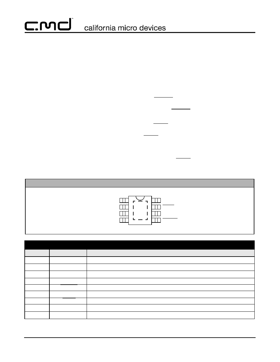
PACKAGE / PINOUT DIAGRAM
Note: This drawing is not to scale.
8-Lead PSOP
1
2
3
4
8
7
6
5
V
CC
V
DDQ
V
TT
GND
SENSE_V
DDQ
FAULT
SENSE_V
TT
EN_DDR
TOP VIEW

©
2004 California Micro Devices Corp. All rights reserved.
11/12/04
430 N. McCarthy Blvd., Milpitas, CA 95035-5112
Tel: 408.263.3214
Fax: 408.263.7846
www.calmicro.com
3
CM3121
PRELIMINARY
Ordering Information
Note 1: Parts are shipped in Tape & Reel form unless otherwise specified.
Specifications
Note 1: The V
DDQ
regulator provides power for both the memory load and the V
TT
regulator, supplying a total of 1.5A to the V
DDQ
and V
TT
outputs. For example, if the V
DDQ
load current is 1.2A, then the maximum V
TT
load current will be 0.3A, regardless
of the actual V
TT
output current rating.
PART NUMBERING INFORMATION
Leads
Package
Standard Finish
Lead-free Finish
Ordering Part
Number
1
Part Marking
Ordering Part
Number
1
Part Marking
8
PSOP-8
CM3121-02SB
CM3121 02SB
CM3121-02SH
CM3121 02SH
ABSOLUTE MAXIMUM RATINGS
PARAMETER
RATING
UNITS
ESD (Human Body Model)
±
2000
V
Pin Voltages
V
CC
EN_DDR,
SENSE_V
DDQ
, SENSE_V
TT
[GND - 0.6] to [+6.5]
[GND - 0.6] to [V
CC
+ 0.6]
V
V
Storage Temperature Range
-40 to +150
∞C
Operating Temperature Range
Ambient
Junction
-40 to +85
0 to +125
∞C
∞C
STANDARD OPERATING CONDITIONS
PARAMETER
RATING
UNITS
Ambient Operating Temperature Range
-40 to +85
∞C
1. V
DDQ
Regulator
DDR-I Supply Voltage V
CC
[V
DDQ
+ 0.3] to 3.6
V
DDR-II Supply Voltage V
CC
2.2 to 2.8
V
Load Current (note 1)
0 to 1500
mA
C
CC
, C
DDQ
10, 10
µ
F
2. V
TT
Regulator
DDR-I Supply Voltage V
DDQ
2.3 to 2.8
V
DDR-II Supply Voltage V
DDQ
1.7 to 1.9
V
DDR-I Load Current
0 to
±
500
mA
DDR-II Load Current
0 to
±
300
mA
C
TT
47
µ
F

©
2004 California Micro Devices Corp. All rights reserved.
4
430 N. McCarthy Blvd., Milpitas, CA 95035-5112
Tel: 408.263.3214
Fax: 408.263.7846
www.calmicro.com
11/12/04
CM3121
PRELIMINARY
Specifications (cont'd)
DDR-I Specifications
ELECTRICAL OPERATING CHARACTERISTICS
(SEE NOTE1)
SYMBOL
PARAMETER
CONDITIONS
MIN
TYP
MAX
UNITS
General Parameters
T
OVER
Shutdown Junction Temperature
-
150
-
∞C
T
HYST
Junction Temp Hysterisis
IC in shutdown
-
25
-
∞C
I
CCN
Normal Mode V
CC
Supply
Current
EN_DDR = logic "0",
EN_CORE =logic "0"
700
1100
µ
A
I
CCQ
Shutdown Mode V
CC
Supply
Current
EN_DDR = logic "1",
V
DDQ
= 0V, V
TT
= 0V
2
10
µ
A
V
IH
EN_DDR Input High Threshold
V
CC
=3.3V
2.0
V
V
IL
EN_DDR Input Low Threshold
V
CC
=3.3V
0.4
V
UVLO
Under Voltage Lock-Out
I
DDQ
= 10mA
1.8
V
t
RISE
V
DDQ
Rise TIme
V
CC
= 3.3V, C
DDQ
= 10
µF
0.5
ms
V
DDQ
Regulator Parameters
V
CC MIN
Input Voltage
V
DDQ
= 2.5V, I
DDQ
= 1.5A,
SENSE_V
DDQ
= 0V, Note 2
2.80
V
V
DDQ DEF
Default Output Voltage Range
I
DDQ
= 0.01A, 2.8V
V
CC
3.6V,
SENSE_V
DDQ
= 0V, Note 2
2.45
2.50
2.55
V
V
DDQ ADJ
Adjustable Output Voltage
Range
V
CC
= 3.6V, SENSE_V
DDQ
tied to
external resistors R1 and R2, Note 2
1.6
2.8
V
V
DDQ LD
Load Regulation
T
A
= 25∞C, V
CC
= 3.3V,
0.01A
I
DDQ
1.0A, Note 2
-
-
2.5
%
V
DDQ LINE
Line Regulation
T
A
= 25∞C, I
DDQ
= 0.01A,
2.8V
V
CC
3.6V, Note 2
-1.0
-
1.0
%
e
N DDQ
Output Noise Voltage
BW = 10Hz - 100kHz, C
DDQ
= 10µF
49
µ
Vrms
I
DDQ LIM
Current Limit
Note 2
1.7
2.0
A
I
DDQ SC
Short Circuit Current
V
DDQ
< 0.3V
0.5
A
©
2004 California Micro Devices Corp. All rights reserved.
11/12/04
430 N. McCarthy Blvd., Milpitas, CA 95035-5112
Tel: 408.263.3214
Fax: 408.263.7846
www.calmicro.com
5
CM3121
PRELIMINARY
Note 1: All parameters specified at T
A
= -40∞C to +85∞C unless otherwise noted.
Note 2: Note that the I
DDQ
current specified is the load current output from the V
DDQ
pin. V
DDQ
also supplies current internally to the
V
TT
regulator when it is sourcing current. The maximum source current can be up to 0.5A. So the maximum total current
from the V
DDQ
regulator is the external V
DDQ
current I
DDQ
added to the maximum V
TT
sourcing current I
TT
. All load currents
are specified as such, but the V
DDQ
current limit is specified at a current just above the total maximum current.
DDR-II Specifications
V
TT
Regulator Parameters
V
TT
Output Voltage Range
V
DDQ
= 2.5V, I
TT
= 0.01A,
1.20
1.25
1.30
V
V
TT REF
Output Voltage Range
V
DDQ
= 2.500V, I
TT
= 0.01A
1.225
1.250
1.275
V
V
TT LD
Load Regulation
T
A
= 25∞C, V
DDQ
= 2.5V,
0.01A
I
TT
±0.5A
-1.0
-
1.0
%
V
TT LINE
Line Regulation
T
A
= 25∞C, I
TT
= 0.01A,
2.8V
V
CC
3.6V, Note 2
-1.0
-
1.0
%
e
N TT
Output Noise Voltage
BW = 10Hz - 100kHz, C
TT
= 10µF
51
µ
Vrms
I
TT LIM
Current Limit
0.6
0.8
A
I
TT SC
Short Circuit Current
V
TT
< 0.3V
0.3
A
ELECTRICAL OPERATING CHARACTERISTICS (CONT'D)
(SEE NOTE1)
ELECTRICAL OPERATING CHARACTERISTICS
(SEE NOTE 3)
SYMBOL
PARAMETER
CONDITIONS
MIN
TYP
MAX
UNITS
General Parameters
T
OVER
Shutdown Junction Temperature
-
150
-
∞C
T
HYST
Junction Temp Hysterisis
IC in shutdown
-
25
-
∞C
I
CCN
Normal Mode V
CC
Supply
Current
EN_DDR = logic "0",
700
1100
µ
A
I
CCQ
Shutdown Mode V
CC
Supply
Current
EN_DDR = logic "1",
V
DDQ
= 0V, V
TT
= 0V
2
10
µ
A
V
IH
EN_DDR Input High Threshold
V
CC
=3.3V
2.0
V
V
IL
EN_DDR Input Low Threshold
V
CC
=3.3V
0.4
V
UVLO
Under Voltage Lock-Out
I
DDQ
= 10mA
1.8
V
t
RISE
V
DDQ
Rise TIme
V
CC
= 3.3V, C
DDQ
= 10
µF
0.5
ms

©
2004 California Micro Devices Corp. All rights reserved.
6
430 N. McCarthy Blvd., Milpitas, CA 95035-5112
Tel: 408.263.3214
Fax: 408.263.7846
www.calmicro.com
11/12/04
CM3121
PRELIMINARY
Note 3: All parameters specified at T
A
= -40∞C to +85∞C unless otherwise noted.
Note 4: Note that the I
DDQ
current specified is the load current output from the V
DDQ
pin. V
DDQ
also supplies current internally to the
V
TT
regulator when it is sourcing current. The maximum source current can be up to 0.5A. So the maximum total current
from the V
DDQ
regulator is the external V
DDQ
current I
DDQ
added to the maximum V
TT
sourcing current I
TT
. All load currents
are specified as such, but the V
DDQ
current limit is specified at a current just above the total maximum current.
Table 1: Truth Table for CM3121
V
DDQ
Regulator Parameters
V
CC MIN
Input Voltage
V
DDQ
= 2.5V, I
DDQ
= 1.5A,
SENSE_V
DDQ
= 0V, Note 4
2.2
V
V
DDQ
Default Output Voltage Range
I
DDQ
= 0.01A,V
CC
= 3.3V,
SENSE_V
DDQ
= 0V, Note 4
1.75
1.80
1.85
V
V
DDQ ADJ
Adjustable Output Voltage
Range
V
CC
= 3.3V, SENSE_V
DDQ
tied to
external resistors R1 and R2, Note 4
1.6
2.8
V
V
DDQ LD
Load Regulation
T
A
= 25∞C, V
CC
= 2.5V,
0.01A
I
DDQ
1.0A, Note 4
-
-
2.5
%
V
DDQ LINE
Line Regulation
T
A
= 25∞C, I
DDQ
= 0.01A,
2.2V
V
CC
2.8V, Note 4
-1.0
-
1.0
%
e
N DDQ
Output Noise Voltage
BW = 10Hz - 100kHz, C
DDQ
= 10µF
49
µ
Vrms
I
DDQ LIM
Current Limit
Note 4
1.7
2.0
A
I
DDQ SC
Short Circuit Current
V
DDQ
< 0.3V
0.5
A
V
TT
Regulator Parameters
V
TT
Output Voltage Range
V
DDQ
= 1.8V, I
TT
= 0.01A,
0.86
0.90
0.94
V
V
TT LD
Load Regulation
T
A
= 25∞C, V
DDQ
= 1.8V,
0.01A
I
TT
±0.3A
-1.0
-
1.0
%
V
TT LINE
Line Regulation
T
A
= 25∞C, I
TT
= 0A,
2.2V
V
CC
2.8V
-1.0
-
1.0
%
e
N TT
Output Noise Voltage
BW = 10Hz - 100kHz, C
TT
= 10µF
51
µ
Vrms
I
TT LIM
Current Limit
0.4
0.6
A
I
TT SC
Short Circuit Current
V
TT
< 0.3V
0.3
A
V
CC
(1)
EN_DDR
V
DDQ OUT
V
TT OUT
2.8V to 3.6V
Low
V
DDQ
V
DDQ
/ 2
X
High
0V
0V
ELECTRICAL OPERATING CHARACTERISTICS (CONT'D)
(SEE NOTE 3)

©
2004 California Micro Devices Corp. All rights reserved.
11/12/04
430 N. McCarthy Blvd., Milpitas, CA 95035-5112
Tel: 408.263.3214
Fax: 408.263.7846
www.calmicro.com
7
CM3121
PRELIMINARY
Performance Information
Power Supply Ripple Rejection
C
CC
= 10
µF, V
CC
= 3.3V, I
LOAD
= 50mA, PSRR measured with 50mV pk-pk sin wave on V
CC
.
Figure 1. V
DDQ
PSRR (V
DDQ
= 2.5V)
Figure 2. V
TT
PSRR (V
TT
= 1.25V)
0
5
10
15
20
25
30
35
40
45
50
10
100
1000
10000
100000
Frequency (Hz)
PSR
R
(
d
B
)
0
10
20
30
40
50
60
10
100
1000
10000
100000
Frequency (Hz)
PSR
R
(
d
B
)

©
2004 California Micro Devices Corp. All rights reserved.
8
430 N. McCarthy Blvd., Milpitas, CA 95035-5112
Tel: 408.263.3214
Fax: 408.263.7846
www.calmicro.com
11/12/04
CM3121
PRELIMINARY
Performance Information (cont'd)
Typical Thermal Characteristics
The overall junction to ambient thermal resistance
(
JA
) for device power dissipation (P
D
) consists prima-
rily of two paths in series. The first path is the junction
to the case (
JC
) which is defined by the package style,
and the second path is case to ambient (
CA
) thermal
resistance which is dependent on board layout. The
final operating junction temperature for any set of con-
ditions can be estimated by the following thermal equa-
tion:
T
JUNC
= T
AMB
+ P
D
(
JC
) + P
D
(
CA
)
= T
AMB
+ P
D
(
JA
)
When a CM3121-02SB/SH (PSOP-8) is mounted on a
double-sided printed circuit board with two square
inches of copper allocated for "heat spreading," the
resulting
JA
is 40
∞
C/W. Based on the over tempera-
ture limit of 150
∞
C with an ambient of 70
∞
C, the avail-
able power of this package will be:
P
D
=
= 2W
PCB Layout Considerations
The CM3121-02SB/SH has a heat spreader attached
to the bottom of the PSOP-8 package in order for heat
to be transferred more easily from the package to the
PCB. The heat spreader is a copper pad of dimensions
just smaller than the package itself. By positioning the
matching pad on the PCB top layer to connect to the
spreader during manufacturing, the heat will be trans-
ferred between the two pads. The drawing below
shows the recommended PCB layout. Note that there
are six vias on either side to allow the heat to dissipate
into the ground and power planes on the inner layers of
the PCB. Vias can be placed underneath the chip, but
this can cause blockage of the solder. The ground and
power planes should be at least 2 sq in. of copper by
the vias. It also helps dissipation if the chip is posi-
tioned away from the edge of the PCB, and not near
other heat-dissipating devices. A good thermal link
from the PCB pad to the rest of the PCB will assure the
best heat transfer from the CM3121 package to ambi-
ent,
JA
, of around 40
∞
C/W.
Figure 3. Recommended Heat Sink PCB Layout
150
∞ C 70∞ C
≠
40
∞ C/ W
---------------------------------------

©
2004 California Micro Devices Corp. All rights reserved.
11/12/04
430 N. McCarthy Blvd., Milpitas, CA 95035-5112
Tel: 408.263.3214
Fax: 408.263.7846
www.calmicro.com
9
CM3121
PRELIMINARY
Application Information
Other Applications
The CM3121 can be used without any external resis-
tors if a V
DDQ
voltage of 2.5V is required by connecting
the SENSE_V
DDQ
pin to GND.
Also in applications where a reference voltage (V
REF
)
is required, a PCB trace directly from the V
TT
pin can
be used. The V
TT
output pin has an error relative to
V
DDQ
/2 of up to +/-25mV, which is well within most
DDR system specs of +/-50mV. This is because the
V
TT
output internally tracks the V
DDQ
output very
closely due to the matched on-chip resistors R that tap
down from the V
DDQ
rail, and the low offset voltage of
the V
TT
regulator. It is recommended that the V
REF
trace be connected directly to the V
TT
pin, to eliminate
noise and ripple on the V
TT
line caused by current
switching
.
Figure 4. Typical Application for the CM3121
V
REF
=1.25V
V
REF
R
R
FAULT
V
TT
=1.25V
V
DDQ
REGULATOR
V
TT
REGULATOR
EN_DDR
V
CC
GND
C
DDQ
DDR
MEMORY
CPU
CORE
+ I/O
C
CC
C
TT
Enable DDR
Memory #
2.8V to 3.6V
SENSE V
TT
V
TT
SENSE V
TT
V
DDQ
SENSE
V
DDQ
CURRENT LIMIT
OVERTEMP
LOW INPUT
©
2004 California Micro Devices Corp. All rights reserved.
10
430 N. McCarthy Blvd., Milpitas, CA 95035-5112
Tel: 408.263.3214
Fax: 408.263.7846
www.calmicro.com
11/12/04
CM3121
PRELIMINARY
Application Information (cont'd)
DDR-II Application
For DDR-II applications, it is recommended that a
lower input voltage than 3.3V be applied to reduce
overall power dissipation. The input voltage can be as
low as 2.1V worst case, so an input voltage of 2.4V
±
10% would be the best input voltage for the least
power dissipation. Also to obtain a V
DDQ
voltage of
1.8V, a resistor divider comprising R1 = 56K and R2 =
130K would result in an output voltage of 1.79V for
V
DDQ
, and a V
TT
of 0.895V.
The maximum current I
DDQ
for the CM3121 in a DDR-
II application is 1.5V, and the maximum for I
TT
is 0.3V.
This should be satisfactory for most DDR- II applica-
tions because the DDR- II memories do not require a
V
TT
, so the only current needed is for either a refer-
ence voltage or a controller input.
.
Figure 5. Minimal CM3132 DDR-II power solution.
V
REF
R
R
FAULT
V
TT
=0.90V
V
DDQ
REGULATOR
V
TT
REGULATOR
EN_DDR
V
CC
GND
C
DDQ
DDR
MEMORY
CPU
CORE
+ I/O
C
CC
C
TT
Enable DDR
Memory #
2.15V to 3.6V
SENSE V
TT
V
TT
SENSE V
TT
V
DDQ
SENSE
V
DDQ
CURRENT LIMIT
OVERTEMP
LOW INPUT
R1
R2
V
DDQ
=1.8V*
* V
DDQ
= 1.25V x
R1 R2
+
R2
----------------------

©
2004 California Micro Devices Corp. All rights reserved.
11/12/04
430 N. McCarthy Blvd., Milpitas, CA 95035-5112
Tel: 408.263.3214
Fax: 408.263.7846
www.calmicro.com
11
CM3121
PRELIMINARY
Mechanical Details
PSOP-8 Mechanical Specifications
Dimensions for CM3121 devices packaged in an 8-
lead PSOP package with a heatspreader are shown
below.
* This is an approximate number which may vary.
**
Centered on package centerline.
Package Dimensions for PSOP-8
PACKAGE DIMENSIONS
Package
PSOP-8
Leads
8
Dimensions
Millimeters
Inches
Min
Max
Min
Max
A
1.30
1.62
0.051
0.064
A
1
0.03
0.10
0.001
0.004
B
0.33
0.51
0.013
0.020
C
0.18
0.25
0.007
0.010
D
4.83
5.00
0.190
0.197
E
3.81
3.99
0.150
0.157
e
1.02
1.52
0.040 0.060
H
5.79
6.20
0.228
0.244
L
0.41
1.27
0.016
0.050
x**
3.30
3.81
0.130
0.150
y**
2.29
2.79
0.090
0.110
# per tube
100 pieces*
# per tape
and reel
2500 pieces
Controlling dimension: inches
Mechanical Package Diagrams
H
TOP VIEW
L
END VIEW
C
e
B
A
A1
SEATING
PLANE
SIDE VIEW
1
2
3
4
8
7
6
5
Pin 1
E
D
H
BOTTOM VIEW
1
2
3
4
8
7
6
5
x
y
y/2
x/2
Marking
D
E
Heat Slug