
© 2004 California Micro Devices Corp. All rights reserved.
02/02/04
430 N. McCarthy Blvd., Milpitas, CA 95035-5112 Tel: 408.263.3214 Fax: 408.263.7846
www.calmicro.com
CM3131
1
Triple Linear Voltage Regulator for DDR-I/-II Memory
Features
∑ Integrated power solution for DDR-I and DDR-II
memory systems with few external components
∑ Three all-linear regulators for V
DDQ
, V
TT
and
V
STBY
power supply applications
∑ Lowest system cost and smallest footprint for
DDR power solutions
∑ V
DDQ
regulator/driver utilizes external N-FET to
provide up to 15A current at 2.5V/1.8V
∑ V
TT
source/sink regulator provides up to 2A at
1.25V for DDR-I systems or 0.65A at 0.9V for
the DDR-II memory controller (not DDR-II
memory)
∑ LDO standby regulator provides up to 500mA at
2.5V for DDR-I and at 1.8V for DDR-II systems
∑ Can be ganged for higher current applications
∑ Over temperature and reverse current protection
∑ Over current protection for V
STBY
and V
TT
regulator
∑ Available in 8 lead and 14 lead PSOP packages
∑ Lead-free
versions
available
Applications
∑ Desktop PCs, notebooks, and workstations
∑ Set top boxes, digital TVs, printers
∑ Embedded
systems
Product Description
The CM3131 family of all-linear regulators provides
an integrated power solution for DDR-I/-II memory
systems in both run-time and standby modes of
operation. The CM3131 is ideal for designs
incorporating both a main 3.3V and a standby (3.3V
or 5V) supply. The CM3131 features three
independent linear regulators for V
DDQ
, V
TT
and V
STBY
supply regulation and will maintain an accuracy of
±1% across the operating temperature range.
The CM3131 is offered in two configurations. The
CM3131-01/11 drives a single external N-FET on a
single V
DDQ
rail. The CM3131-02 drives two external
unmatched N-FETs on two V
DDQ
rails. Each V
DDQ
rail
incorporates an adjustment pin (SENSE) to enable
setting V
DDQ
in the 2.2V to 2.8V range, supporting
DIMMs with different supply requirements or DDR-II
type devices.
The CM3131-01/11 is available in 8-lead PSOP
package and the CM3131-02 is available in 14-lead
PSOP package.
The CM3131 devices are also available with optional
lead-free finishing.
Electrical Schematic
© 2004 California Micro Devices Corp. All rights reserved.
02/02/04
430 N. McCarthy Blvd., Milpitas, CA 95035-5112 Tel: 408.263.3214 Fax: 408.263.7846
www.calmicro.com
CM3131
2
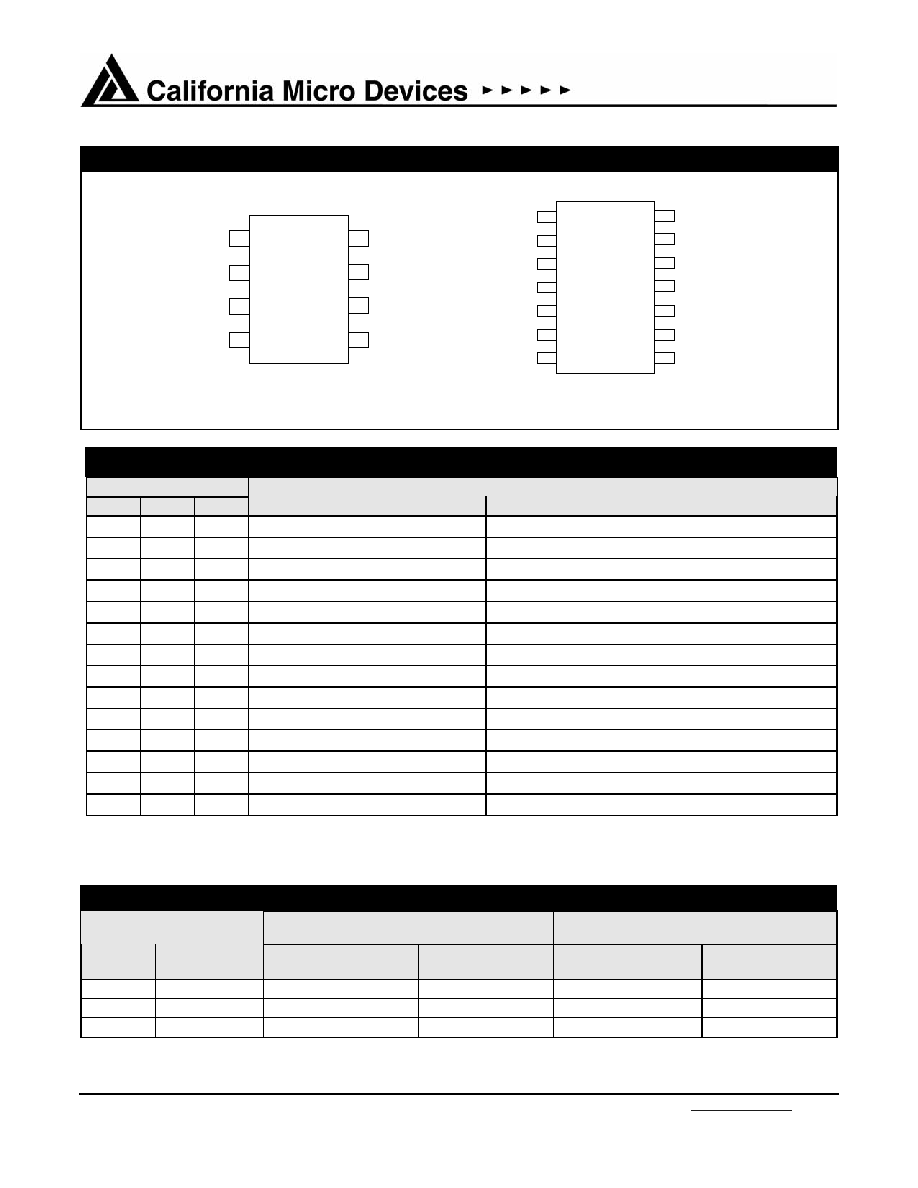
PACKAGE / PINOUT DIAGRAM
Note: These drawings are not to scale.
PIN DESCRIPTIONS
PART NUMBER
-01
-11
-02
NAME
DESCRIPTION
1 1 13
V
DDQ
/ V
DDQ1
V
DDQ
input for V
REF
and V
DDQ
Output in Standby
2 2 14
V
TT
V
TT
Output for termination resistors
1
NC
No
connection
3 3 2
GND
Ground
4
3
SEL
Select Input, active low
4
NC
No
connection
4
7
EN
Enable Input, active high
5
5
5
SENSE / SENSE1
Sense Input, Adjusts V
DDQ
Rail
6 6 6
V
CC
3.3V Main Input Supply
7 7 8
V
STBY
3.3V or 5V Standby Input Supply
8
8
9
DRIVE / DRIVE1
Drive Output for V
DDQ
External n-FET
10
DRIVE2
Drive Output for V
DDQ
External n-FET
11
SENSE2
Sense Input, Adjusts V
DDQ
Rail
12
V
DDQ 2
V
DDQ
Input for V
REF
and V
DDQ
Output in Standby
Ordering Information
PART NUMBERING INFORMATION
STANDARD FINISH
LEAD-FREE FINISH
PINS
PACKAGE
ORDERING PART
NUMBER
1
PART
MARKETING
ORDERING
PART NUMBER
1
PART
MARKING
8 PSOP-8 CM3131-01SB CM3131-01SB
CM3131-01SH
CM3131-01SH
8 PSOP-8 CM3131-11SB CM3131-11SB
CM3131-11SH
CM3131-11SH
14 PSOP-14 CM3131-02SB CM3131-02SB CM3131-02SH CM3131-02SH
Note 1: Parts are shipped in Tape & Reel form unless otherwise specified.
V
DDQ
V
TT
GND
SEL/EN
DRIVE
V
STBY
V
CC
SENSE
CM3131-01/11
PSOP-8
TOP VIEW
PSOP-14
V
TT
V
DDQ1
V
DDQ2
SENSE2
DRIVE2
DRIVE1
V
STBY
CM3131-02
TOP VIEW
NC
GND
SEL
NC
SENSE1
V
CC
EN
© 2004 California Micro Devices Corp. All rights reserved.
02/02/04
430 N. McCarthy Blvd., Milpitas, CA 95035-5112 Tel: 408.263.3214 Fax: 408.263.7846
www.calmicro.com
CM3131
3
Functional Description
The CM3131-01 / -11 and CM3131-02 provide
power for DDR-I/DDR-II memories from three
voltage regulators on-chip with either one or two
external N-FETs respectively. There is an over-
temperature thermal shutdown if any of the
regulators overheat. Each regulator has reverse
current protection in the event of any being shut
down.
The linear regulator-driver/s with external N-FET/s
can provide up to 15A at 2.5V/1.8V for the V
DDQ
of
DDR-I/-II memory, from an input supply voltage of
2.8V-3.6V. An external feedback resistor divider,
connected to the SENSE1 pin, enables selection of
V
DDQ
output voltages from 2.2V to 2.8V for use with
DDR-I memories requiring other than 2.5V for V
DDQ
.
V
DDQ
= 1.25V x (R1+R2)/R2. When SENSE1 is
connected to GND or left open, V
DDQ
is fixed at
2.50V (and VTT at 1.25V). For DDR-II operation,
V
DDQ
can be set from 1.7V to 1.9V.
The V
TT
regulator is a linear source-sink regulator
powered from the V
DDQ
output that supplies the V
TT
supply required by DDR-I memory termination
resistors. This regulator sinks or sources up to 2A at
1.25V to or from the DDR-I bus termination resistors.
For DDR-II applications, the regulator sinks or
sources 0.65A at 0.9V. The V
TT
output voltage
accurately tracks V
DDQ
/2 to 1%. When there is no
V
CC
provided, V
TT
is powered down and its output is
0V. This regulator has overload current limiting of
2.5A.
The standby regulator is a LDO regulator that is
powered from a standby voltage, V
STBY
, of 3.3V or
5V, and supplies a regulated output of up to 500mA
to the V
DDQ
of the DDR memory to enable it to retain
its contents during the standby mode. It provides
2.5V for DDR-I and 1.8V for DDR-II.
The CM3131-01 and CM3131-11 differ with regards
the selection of truth table for determining which S0-
S5 sequencing matrix the chip is set for. The
CM3131-02 has both EN and SEL pins to more
accurately define each Sx stage without monitoring
the V
CC
or V
STBY
voltages.
Two CM3131s can be ganged together to provide
V
DDQ
power to dual channels of DDR memory, and
the memory controller chip of any chip set.
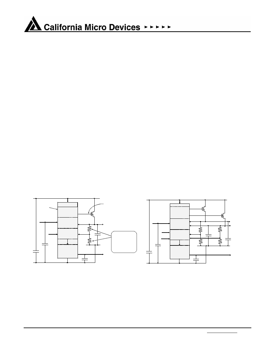
V
TT
Linear
Source-Sink
V
TT
Reg
V
DDQ
V
DDQ
V
DDQ
LDO Drive
SEL / EN
C
CC
C
SBY
C
TT
C
DDQ
5V
STBY
/ 3.3V
STBY
GND
GND
2.8V / 3.0V / 3.3V for DDR-I,
2.2V /2.5V / 3.3V for DDR-II
DRIVE
SENSE
V
DDQ
LDO
V
DDQ
/ V
TT
Control
V
DDQ
FET
V
TT
V
CC
Only needed for
DDR-I if V
DDQ
is
not 2.5V, e.g. 2.6V
or 2.7V.
Set to 1.7V to
1.9V for DDR-II
PSOP-8
Internal V
SBY
voltage
doubler ensures V
G
> 5.3V
Drives any N-FET with C
GS
<1200pF
R1
R2
V
TT
Linear
Source-Sink
V
TT
Reg
V
DDQ
V
DDQ1
V
DDQ
LDO Drives
C
CC
C
SBY
C
TT
C
DDQ2
5V
STBY
/ 3.3V
STBY
GND
DRIVE1
C
DDQ1
DRIVE2
V
DDQ2
SENSE1
SENSE2
V
DDQ1
V
DDQ2
V
DDQ
LDOs
V
DDQ
/ V
TT
Control
SEL
GND
N-FET1
N-FET2
V
TT
2.8V / 3.0V / 3.3V for DDR-I,
2.2V /2.5V / 3.3V for DDR-II
EN
V
CC
CM3131-02
R1
R2
R3
R4
Examples of Single and Dual N-FET Drive Configurations
CM3131-01/11

© 2004 California Micro Devices Corp. All rights reserved.
02/02/04
430 N. McCarthy Blvd., Milpitas, CA 95035-5112 Tel: 408.263.3214 Fax: 408.263.7846
www.calmicro.com
CM3131
4
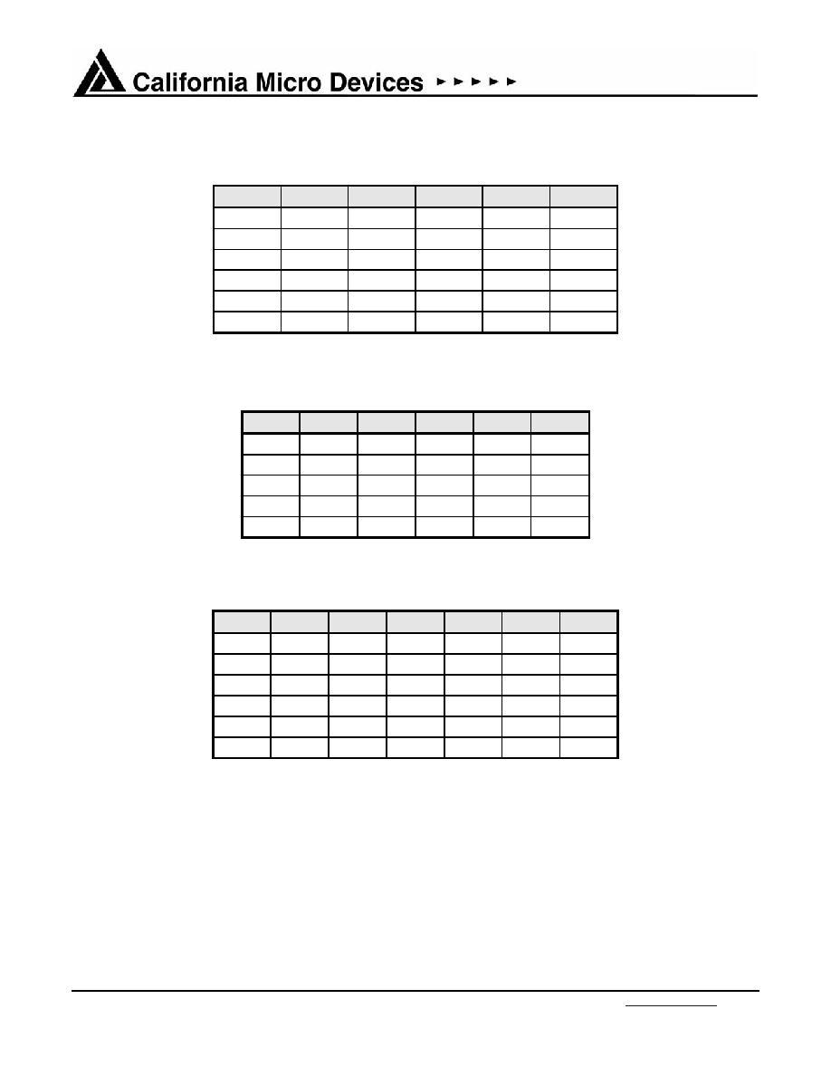
Functional Description (cont'd)
V
CC
V
STBY
SEL
V
DDQ 1,2
V
TT
3V/3.3V 5V/3.3V
ON
V
DDQ
V
DDQ
/ 2
X 5V/3.3V
OFF
V
DDQ STBY
0V
<V
CC MIN
X ON 0V 0V
X <V
STBY MIN
OFF 0V 0V
Truth Table for CM3131-01
S to R
V
CC
V
STBY
SEL
V
DDQ OUT
V
TT OUT
S0 3V/3.3V
5V/3.3V ON V
DDQ
V
DDQ
/ 2
S1 3V/3.3V
5V/3.3V ON V
DDQ
V
DDQ
/ 2
S2 3V/3.3V
5V/3.3V ON V
DDQ
V
DDQ
/ 2
S3 3V/3.3V
5V/3.3V OFF
V
DDQ STBY
0V
S4 <V
CC MIN
5V/3.3V OFF
0V
0V
S5 <V
CC MIN
5V/3.3V OFF
0V
0V
Sequencing Matrix for CM3131-01 for Suspend to RAM operation
No S to R V
CC
V
STBY
SEL
V
DDQ OUT
V
TT OUT
S0 3V/3.3V
5V/3.3V ON V
DDQ
V
DDQ
/ 2
S1 3V/3.3V
5V/3.3V ON V
DDQ
V
DDQ
/ 2
S2 3V/3.3V
5V/3.3V ON V
DDQ
V
DDQ
/ 2
S3 <V
CC MIN
5V/3.3V ON
0V
0V
S4 <V
CC MIN
5V/3.3V ON
0V
0V
S5 <V
CC MIN
5V/3.3V ON
0V
0V
Sequencing Matrix for CM3131-01 for Suspend to RAM Not Supported
V
CC
V
STBY
EN
V
DDQ OUT
V
TT OUT
3V/3.3V 5V/3.3V
ON
V
DDQ
V
DDQ
/ 2
<V
CC MIN
5V/3.3V ON V
DDQ STBY
0V
<V
CC MIN
X OFF 0V 0V
X <V
STBY MIN
OFF 0V 0V
Truth Table for CM3131-11
© 2004 California Micro Devices Corp. All rights reserved.
02/02/04
430 N. McCarthy Blvd., Milpitas, CA 95035-5112 Tel: 408.263.3214 Fax: 408.263.7846
www.calmicro.com
CM3131
5
Functional Description (cont'd)
S to R
V
CC
V
STBY
EN
V
DDQ OUT
V
TT OUT
S0 3V/3.3V
5V/3.3V ON V
DDQ
V
DDQ
/ 2
S1 3V/3.3V
5V/3.3V ON V
DDQ
V
DDQ
/ 2
S2 3V/3.3V
5V/3.3V ON V
DDQ
V
DDQ
/ 2
S3 <V
CC MIN
5V/3.3V ON V
DDQ STBY
0V
S4 <V
CC MIN
5V/3.3V OFF
0V
0V
S5 <V
CC MIN
5V/3.3V OFF
0V
0V
Sequencing Matrix for CM3131-11 for Suspend to RAM operation
V
CC
V
STBY
SEL
EN
V
DDQ OUT
V
TT OUT
3V/3.3V 5V/3.3V
ON
ON
V
DDQ
V
DDQ
/ 2
<V
CC MIN
5V/3.3V OFF
ON V
DDQ STBY
0V
X <V
STBY MIN
OFF ON 0V 0V
0V X ON
ON 0V 0V
<V
CC MIN
X X
OFF
0V
0V
Truth Table for CM3131-02
Table 3
V
CC
V
STBY
SEL
EN
V
DDQ OUT
V
TT OUT
S0 3V/3.3V
5V/3.3V ON ON V
DDQ
V
DDQ
/ 2
S1 3V/3.3V
5V/3.3V ON ON V
DDQ
V
DDQ
/ 2
S2 3V/3.3V
5V/3.3V ON ON V
DDQ
V
DDQ
/ 2
S3 <V
CC MIN
5V/3.3V OFF
ON V
DDQ STBY
0V
S4 <V
CC MIN
X ON
OFF
0V 0V
S5 <V
CC MIN
X ON
OFF
0V 0V
Sequencing Matrix for CM3131-02 for Suspend to RAM operation
© 2004 California Micro Devices Corp. All rights reserved.
02/02/04
430 N. McCarthy Blvd., Milpitas, CA 95035-5112 Tel: 408.263.3214 Fax: 408.263.7846
www.calmicro.com
CM3131
6
Specifications
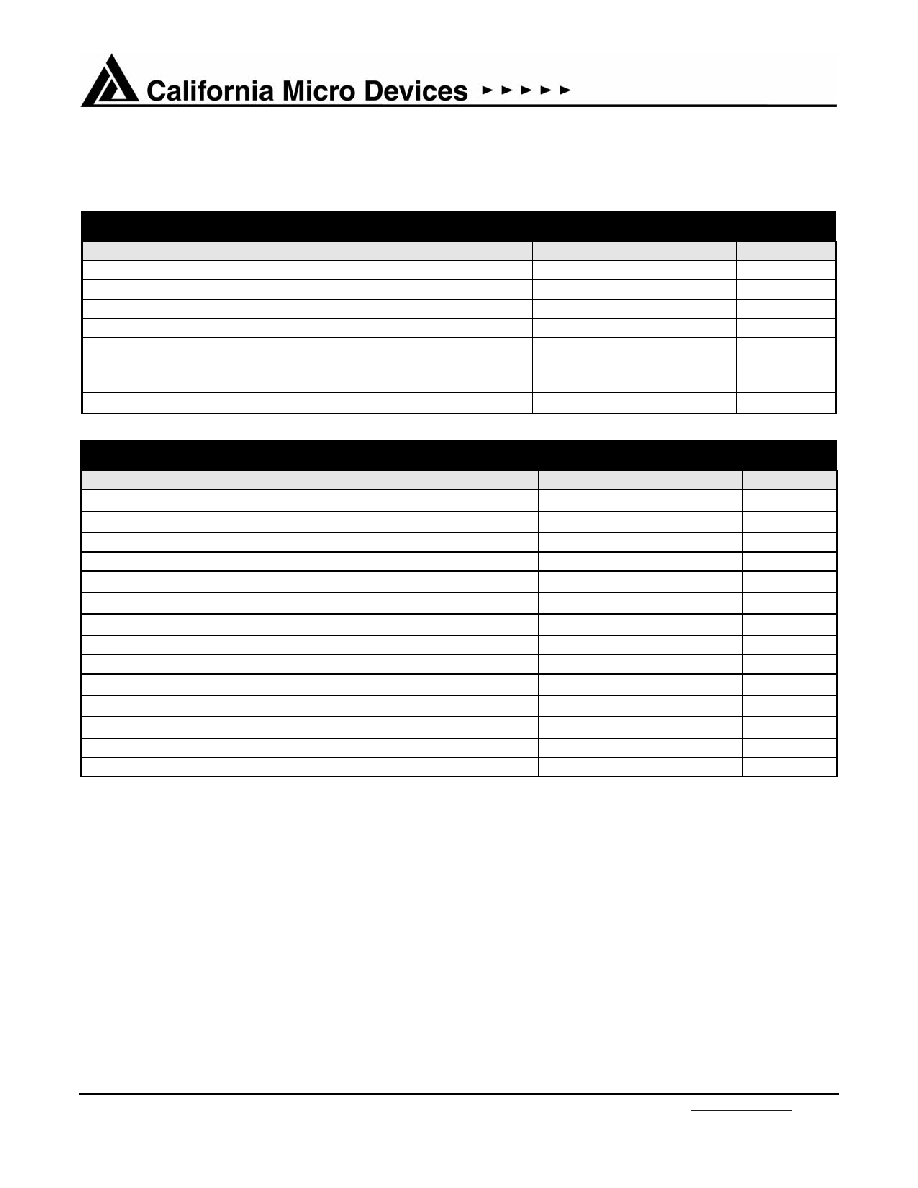
ABSOLUTE MAXIMUM RATINGS
PARAMETER
RATING
UNITS
ESD (Human Body Model)
± 2000
V
V
CC
, V
STBY
, DRIVEx
(GND ≠ 0.6) to (+6.5)
V
SEL, SENSEx
(GND ≠ 0.6) to (V
CC
+ 0.6)
V
V
DDQX
, V
TT
(GND ≠ 0.6) to (V
CC
+ 0.6)
V
Operating Temperature Range
Ambient
0 to +70
∞C
Junction
0 to +125
∞C
Storage Temperature Range
-40 to +150
∞C
STANDARD OPERATING CONDITIONS
PARAMETER
RATING
UNITS
Temperature Range (Ambient)
0 to +70
∞C
1. V
DDQ
Regulator-Driver
Supply Voltage V
CC
2.8 to 3.6
V
Load Current
0 to 15
A
C
CC
, C
DDQ
4.7, 220
µF
2. V
TT
Regulator
Supply Voltage V
DDQ
1.8 or 2.5
V
Load Current
0 to +/- 0.9 or +/- 2.0
A
C
TT
220
µF
3, V
STBY
Regulator
Supply Voltage V
STBY
3.0
to
5.5
V
Load Current
0 to 500
mA

© 2004 California Micro Devices Corp. All rights reserved.
02/02/04
430 N. McCarthy Blvd., Milpitas, CA 95035-5112 Tel: 408.263.3214 Fax: 408.263.7846
www.calmicro.com
CM3131
7
Specifications (cont'd)
ELECTRICAL OPERATING CHARACTERISTICS
(SEE NOTE 1)
SYMBOL
PARAMETER
CONDITIONS
MIN
TYP
MAX
UNITS
General Parameters
T
OVER
Shutdown
Junction
Temperature
-
150
-
∞C
V
DDQ
Regulator/Driver Parameters (with FDP6030L or similar MOSFET as an external transistor)
V
CC MIN
Input
Voltage
V
DDQ
= 2.5V, I
DDQ
= 6A,
each channel, SENSE = 0V
2.80
V
V
DDQ
Output Voltage Range
I
DDQ
= 2.5A, V
CC
= 3.3V,
SENSE = 0V
2.45 2.50 2.55
V
V
DRIVE H 5
DRIVE
High
Output
Voltage
V
STBY
= 5V, V
CC
= 3.3V
9.50
V
V
DRIVE H 3
DRIVE
High
Output
Voltage
V
STBY
= 3.3V, V
CC
= 3.3V
6.1
V
C
LOAD
External
FET
Gate
Capacitance
V
STBY
= 5V, V
CC
= 3.3V
1200
pF
t
RISE
DRIVE Voltage Rise
Time
V
STBY
= 5V, V
CC
= 3.3V,
C
LOAD
= 1200pF
2.5
ms
V
DDQ LOAD
Load Regulation @
25
∞C
V
CC
= 3.3V, I
DDQ
= 0.1A to 6A
each channel
-1.0 - 1.0 %
V
DDQ LINE
Line Regulation @ 25
∞C
I
DDQ
= 2.5A, V
CC
= 2.8V to
3.6V
-1.0 - 1.0 %
V
TT
Regulator Parameters
V
TT
Output Voltage Range
V
DDQ
= 2.50V, I
TT
= 0A
1.20
1.25
1.30
V
V
TT LOAD
Load Regulation @ 25C
I
TT
= 0.1A to 2A, V
DDQ
= 2.5V
-1.0
-
1.0
%
V
TT LINE
Line Regulation @ 25C
I
TT
= 0A, V
CC
= 2.8V to 3.6V
-1.0
-
1.0
%
I
TT LIM
Current
Limit
2.3 A
I
TT SC
Short Circuit Current
Limit
V
TT
< 1V
0.6
A
V
STBY
Regulator Parameters
V
DDQ STBY
Output Voltage Range
I
DDQ
=150mA, V
STBY
= 5V,
SENSE =0V
2.45 2.50 2.55
V
V
DDQSB LD
Load Regulation @ 25C
I
DDQ
= 10mA to 500mA,
V
STBY
= 5V
-1.0 - 1.0 %
V
DDQ SBLN
Line Regulation @ 25C
I
DDQ
= 150mA,
V
STBY
= 3.0V to 5.5V
-1.0 - 1.0 %
V
DROPOUT
Dropout
Voltage
I
DDQ
= 250mA, each channel
250
450 mV
I
STBY LIM
Overload Current Limit
400 mA
I
STBY SC
Short Circuit Current
Limit
V
DDQ
< 1V
170 mA
Note 1: All parameters specified at T
A
= 0
∞
C to +70
∞
C unless otherwise noted.

© 2004 California Micro Devices Corp. All rights reserved.
02/02/04
430 N. McCarthy Blvd., Milpitas, CA 95035-5112 Tel: 408.263.3214 Fax: 408.263.7846
www.calmicro.com
CM3131
8
Specifications (cont'd)
ELECTRICAL OPERATING CHARACTERISTICS (Cont'd)
SYMBOL
PARAMETER
CONDITIONS
MIN
TYP
MAX
UNITS
All Regulators
I
CCN
Normal Mode V
CC
Supply Current
Normal mode (S0-S2)
(V
DDQ1,2
=V
DDQ
,V
TT
=V
DDQ
/2)
5
µA
I
STBYN
Normal Mode V
STBY
Supply Current
Normal mode (S0-S2)
(V
DDQ1,2
=V
DDQ
,V
TT
=V
DDQ
/2)
1650
2450
µA
I
STBYS
Standby Mode V
STBY
Supply Current
Standby mode (S3)
(V
DDQ1,2
=V
DDQSTBY
,V
TT
=0)
550
850
µA
I
STBYQ
Shutdown
Mode
Quiescent Current
Shutdown mode (S4-S5)
(V
DDQ1,2
=0
,V
TT
=0)
70
120
µA
© 2004 California Micro Devices Corp. All rights reserved.
02/02/04
430 N. McCarthy Blvd., Milpitas, CA 95035-5112 Tel: 408.263.3214 Fax: 408.263.7846
www.calmicro.com
CM3131
9
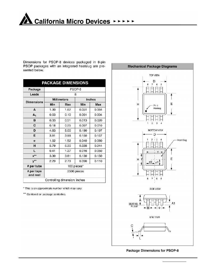
Mechanical Details
8-lead PSOP Package Dimensions

© 2004 California Micro Devices Corp. All rights reserved.
02/02/04
430 N. McCarthy Blvd., Milpitas, CA 95035-5112 Tel: 408.263.3214 Fax: 408.263.7846
www.calmicro.com
CM3131
10
Mechanical Details (cont'd)
14-lead PSOP Package Dimensions