 | –≠–ª–µ–∫—Ç—Ä–æ–Ω–Ω—ã–π –∫–æ–º–ø–æ–Ω–µ–Ω—Ç: CM3132 | –°–∫–∞—á–∞—Ç—å:  PDF PDF  ZIP ZIP |

©
2004 California Micro Devices Corp. All rights reserved.
10/13/04
430 N. McCarthy Blvd., Milpitas, CA 95035-5112
Tel: 408.263.3214
Fax: 408.263.7846
www.calmicro.com
1
CM3132
PRELIMINARY
Triple Linear Voltage Regulator for DDR-I Memory and CPU
Features
∑
Fully integrated power solution for a CPU/SOC
core and DDR-I memory ICs
∑
Lowest system cost and smallest footprint with just
three external output capacitors
∑
Three linear regulators for V
CORE
(1.5A), V
DDQ
(1.5A), and V
TT
(0.5A, source-sink)
∑
V
DDQ
= 2.5V, V
TT
= V
DDQ
/2
±
25mV
∑
V
CORE
is adjustable, with a default output of 1.5V
∑
Over-temperature and reverse current protection
∑
Overcurrent protection for all regulators
∑
PSOP-8 package with integrated heat spreader
∑
Lead-free version available
Applications
∑
Core CPU and DDR-I memory power for:
-
Set Top Boxes, DVD Players, Games
-
Digital TVs, Flat Panel Displays
-
Printers, Digital Projectors
-
Embedded systems
-
Communications systems
Product Description
The CM3132 provides an integrated power solution for a
CPU core and DDR-I memory for consumer and other
embedded applications. It features three independent linear
regulators for V
CORE
, V
DDQ
and V
TT
supply regulation. The
default voltage for V
CORE
is 1.5V. The SENSE_CORE pin
can be tied to GND for the default voltage, or through a
resistor divider for setting the CPU core in the range 1.2V to
1.8V. V
DDQ
is internally set to 2.50V and the V
TT
voltage is
always half the V
DDQ
voltage. A capacitor should be con-
nected to each of the three outputs.
There are two enable pins, EN_CORE and EN_DDR. When
EN_CORE is set high, the CORE regulator is disabled.
When EN_DDR is set high, the two DDR regulators are dis-
abled to minimize overall system power dissipation when
memory is in standby mode. These two enable pins allow
power sequencing of the DDR and CORE regulator blocks
independently.
The CM3132 is available in a PSOP-8 package that has
excellent thermal dissipation. It is available with optional
lead-free finishing.
V
REF
R
R
V
REF
SENSE_CORE
V
TT
=1.25V
V
DDQ
= 2.5V
V
DDQ
REGULATOR
V
TT
REGULATOR
V
CORE
REGULATOR
V
CORE
EN_DDR
V
CC
EN_CORE
GND
C
DDQ
DDR
MEMORY
V
REF
=1.25V
C
CORE
CPU
CORE
+ I/O
C
VCC
R3
R4
C
TT
Enable DDR
Memory #
Enable CORE#
2.8V to 3.3V
V
REF
R
R
V
REF
SENSE_CORE
V
TT
V
DDQ
V
DDQ
REGULATOR
V
TT
REGULATOR
V
CORE
REGULATOR
V
CORE
EN_DDR
V
CC
EN_CORE
GND
Typical Application Circuit
Circuit Schematic

©
2004 California Micro Devices Corp. All rights reserved.
2
430 N. McCarthy Blvd., Milpitas, CA 95035-5112
Tel: 408.263.3214
Fax: 408.263.7846
www.calmicro.com
10/13/04
CM3132
PRELIMINARY
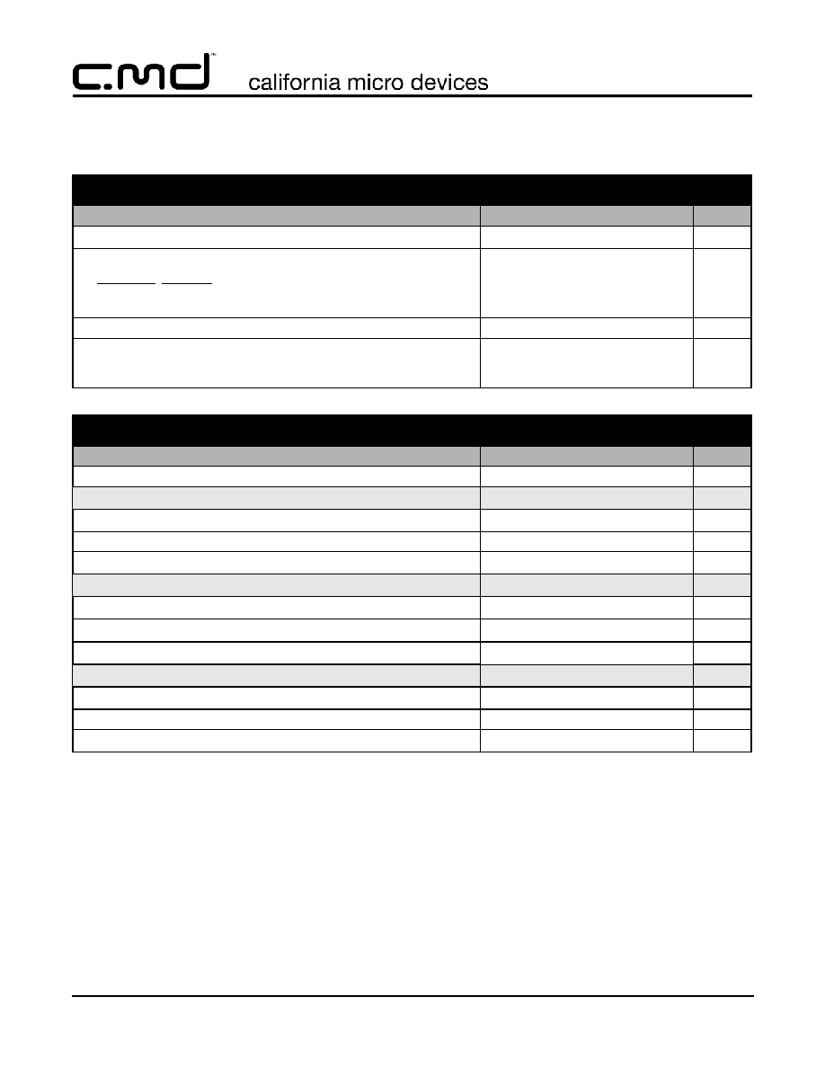
Ordering Information
Note 1: Parts are shipped in Tape & Reel form unless otherwise specified.
PACKAGE / PINOUT DIAGRAM
Note: This drawing is not to scale.
8-Lead PSOP
1
2
3
4
8
7
6
5
V
CORE
V
CC
V
DDQ
V
TT
SENSE_CORE
GND
EN_CORE
EN_DDR
TOP VIEW
PIN DESCRIPTIONS
PSOP-8
NAME
DESCRIPTION
LEAD
1
V
CORE
V
CORE
output.
2
V
CC
Input supply.
3
V
DDQ
V
DDQ
output.
4
V
TT
V
TT
output for termination resistors or V
REF
5
EN_DDR
Enable DDR power. Active low input.
6
EN_CORE
Enable V
CORE
. Active low input.
7
GND
Ground reference.
8
SENSE_CORE
Sense input. Adjusts V
CORE
output voltage using external resistor divider. When tied to
GND, V
CORE
= 1.5V.
PAD
GND
Tied to ground reference.
PART NUMBERING INFORMATION
Leads
Package
Standard Finish
Lead-free Finish
Ordering Part
Number
1
Part Marking
Ordering Part
Number
1
Part Marking
8
PSOP-8
CM3132-02SB
CM3132 02SB
CM3132-02SH
CM3132 02SH
©
2004 California Micro Devices Corp. All rights reserved.
10/13/04
430 N. McCarthy Blvd., Milpitas, CA 95035-5112
Tel: 408.263.3214
Fax: 408.263.7846
www.calmicro.com
3
CM3132
PRELIMINARY
Specifications
ABSOLUTE MAXIMUM RATINGS
PARAMETER
RATING
UNITS
ESD (Human Body Model)
±
2000
V
Pin Voltages
V
CC
EN_CORE, EN_DDR, SENSE_CORE
V
DDQ
, V
TT
[GND - 0.6] to [+6.5]
[GND - 0.6] to [V
CC
+ 0.6]
[GND - 0.6] to [V
CC
+ 0.6]
V
V
V
Storage Temperature Range
-40 to +150
∞C
Operating Temperature Range
Ambient
Junction
0 to +85
0 to +125
∞C
∞C
STANDARD OPERATING CONDITIONS
PARAMETER
RATING
UNITS
Ambient Operating Temperature Range
0 to +85
∞C
1. V
DDQ
Regulator
DDR-I Supply Voltage V
CC
[V
DDQ
+ 0.3] to 3.6
V
Load Current
0 to 1500
mA
C
CC
, C
DDQ
10, 10
µ
F
2. V
TT
Regulator
DDR-I Supply Voltage V
DDQ
2.3 to 2.8
V
DDR-I Load Current
0 to
±
500
mA
C
TT
47
µ
F
3. V
CORE
Regulator
Core Supply Voltage V
CC
[V
DDQ
or V
CORE
+ 0.3] to 3.6
V
DDR-I Load Current
0 to 1500
mA
C
CORE
10
µ
F

©
2004 California Micro Devices Corp. All rights reserved.
4
430 N. McCarthy Blvd., Milpitas, CA 95035-5112
Tel: 408.263.3214
Fax: 408.263.7846
www.calmicro.com
10/13/04
CM3132
PRELIMINARY
Specifications (cont'd)
ELECTRICAL OPERATING CHARACTERISTICS
(SEE NOTE1)
SYMBOL
PARAMETER
CONDITIONS
MIN
TYP
MAX
UNITS
General Parameters
T
OVER
Shutdown Junction Temperature
-
150
-
∞C
T
HYST
Junction Temp Hysterisis
IC in shutdown
-
25
-
∞C
I
CCN
Normal Mode V
CC
Supply
Current
EN_DDR = logic "0",
EN_CORE =logic "0"
400
800
µ
A
I
CCQ
Shutdown Mode V
CC
Supply
Current
EN_DDR = logic "1",
EN_CORE =logic "1"
2
10
µ
A
I
SENSE IN
SENSE_CORE Input Current
V
SENSE_CORE
=0.6V
0.1
1.0
µ
A
V
IH
EN_DDR, EN_CORE Input
High Threshold
V
CORE
=3.3V
2.0
V
V
IL
EN_DDR, EN_CORE Input
Low Threshold
V
CORE
=3.3V
0.4
V
UVLO
Under Voltage Lock-Out
I
DDQ
= 10mA
1.8
V
t
RISE
V
DDQ
, V
CORE
Rise TIme
V
CC
= 3.3V, C
LOAD
= 10
µF
0.5
ms
V
DDQ
Regulator Parameters
V
CC MIN
Input Voltage
V
DDQ
= 2.5V, I
DDQ
= 1.5A, Note 2
2.80
V
V
DDQ DEF
Default Output Voltage
I
DDQ
= 0.01A, 2.8V
V
CC
3.6V,
Note 2
2.45
2.50
2.55
V
V
DDQ LD
Load Regulation
T
A
= 25∞C, V
CC
= 3.3V,
0.01A
I
DDQ
1.5A, Note 2
-
-
2.5
%
V
DDQ LINE
Line Regulation
T
A
= 25∞C, I
DDQ
= 0.01A,
2.8V
V
CC
3.6V, Note 2
-1.0
-
1.0
%
e
N DDQ
Output Noise Voltage
BW = 10Hz - 100kHz, C
DDQ
= 10µF
49
µ
Vrms
I
DDQ LIM
Current Limit
Note 2
1.7
2.0
A
I
DDQ SC
Short Circuit Current
V
DDQ
< 0.3V
0.5
A

©
2004 California Micro Devices Corp. All rights reserved.
10/13/04
430 N. McCarthy Blvd., Milpitas, CA 95035-5112
Tel: 408.263.3214
Fax: 408.263.7846
www.calmicro.com
5
CM3132
PRELIMINARY
Note 1: All parameters specified at T
A
= 0∞C to +85∞C unless otherwise noted.
Note 2: Note that the I
DDQ
current specified is the load current output from the V
DDQ
pin. V
DDQ
also supplies current internally to the
V
TT
regulator when it is sourcing current. The maximum source current can be up to 0.5A.The maximum total current from
the V
DDQ
regulator is the external V
DDQ
current I
DDQ
added to the maximum V
TT
sourcing current I
TT
. All load currents are
specified as such, but the V
DDQ
current limit is specified at a current just above the total maximum current.
Note 3: V
CORE
regulator only. Refer to V
DDQ
regulator parameters for V
DDQ
regulator.
Note 4: V
CORE
= 1.15V X (1 +
)
Table 1: Truth Table for CM3132
V
TT
Regulator Parameters
V
TT
Output Voltage Range
V
DDQ
= 2.5V, I
TT
= 0.01A,
I
DDQ
= 0A
1.20
1.25
1.30
V
V
TT REF
Output Voltage Range
V
CC
= 0V, V
DDQ
= 2.500V,
I
TT
= 0.01A
1.225
1.250
1.275
V
V
TT LD
Load Regulation
T
A
= 25∞C, V
DDQ
= 2.5V,
0.01A
I
TT
±0.5A
-1.0
-
1.0
%
e
N TT
Output Noise Voltage
BW = 10Hz - 100kHz, C
TT
= 10µF
51
µ
Vrms
I
TT LIM
Current Limit
0.6
0.8
A
I
TT SC
Short Circuit Current
V
TT
< 0.7V
0.3
A
V
CORE
Regulator Parameters
V
CC MIN
Input Voltage
V
CORE
= 1.5V, I
CORE
= 1.5A,
SENSE_CORE = 0V, Note 3
2.2
V
V
CORE DEF
Default Output Voltage Range
V
CC
= 3.3V, I
CORE
= 0.01A,
SENSE_CORE = 0V
1.45
1.50
1.55
V
V
CORE ADJ
Adjustable Output Voltage
Range
V
CC
= 3.3V, SENSE_CORE from
resistors R3 & R4, Note 4
1.2
1.8
V
V
CORE LD
Load Regulation
T
A
= 25∞C, V
CC
= 3.3V,
0.01A
I
CORE
±1.5
-
-
2.5
%
V
CORE LINE
Line Regulation
T
A
= 25∞C, 2.8V
V
CC
3.6V,
I
CORE
= 0.01A
-1.0
-
1.0
%
e
N CORE
Output Noise Voltage
BW = 10Hz - 100kHz, C
CORE
= 47µF
59
µ
Vrms
I
CORE LIM
Current Limit
1.7
2.0
A
I
CORE SC
Short Circuit Current
V
CORE
< 0.3V
0.5
A
VCC(1)
EN_DDR
V
DDQ OUT
V
TT OUT
2.8V to 3.6V
Low
V
DDQ
V
DDQ
/ 2
X
High
0V
0V
ELECTRICAL OPERATING CHARACTERISTICS (CONT'D)
(SEE NOTE1)
R3
R4
--------