© 2004 California Micro Devices Corp. All rights reserved.
04/22/04
430 N. McCarthy Blvd., Milpitas, CA 95035-5112
Tel: 408.263.3214
Fax: 408.263.7846 www.calmicro.com
1
CM3196
2A Sink/Source DDR-I, -II Bus Termination Regulator
Features
∑
Ideal for DDR-I, -II V
TT
applications
∑
Sinks and sources 2A for DDR-I, 0.6A for DDR-II
∑
Shutdown input to support ACPI states
∑
Operates down to 1.5V input voltage
∑
Integrated power MOSFETs
∑
Overcurrent protection
∑
Over temperature protection
∑
Excellent accuracy
V
TT
= V
REF
± 30mV
V
TT
= V
DDQ
/2 ± 2%
∑
8-pin SOIC or PSOP package
∑
Lead-free versions available
Applications
∑
DDR-I, -II memory termination
∑
Active termination buses
∑
Graphics card memory termination
Product Description
The CM3196 is a sinking and sourcing regulator specif-
ically designed for DDR-I, -II V
TT
bus termination. The
output voltage accurately tracks V
DDQ
/2.
For DDR-I it
can source and sink current up to 2A with a load regu-
lation of 0.5%. This current adequately serves both sin-
gle and dual channel DDR-I memory systems. For
power conscious notebook applications, the CM3196
also operates from a V
DDQ
of 1.5V or 1.8V with less
current drive. For DDR-II applications, the CM3196
provides up to 0.6A at 0.9V to drive the memory con-
troller V
TT.
For boards which support Suspend to RAM (STR)
functionality, the CM3196 provides a Shutdown (SD)
pin. When SD is set low, V
TT
will be in tri-state mode,
causing the output to go high impedance. In this mode,
CM3196 power is saved by significantly reducing the
quiescent current. V
REF
voltage remains V
DDQ
/2.
The CM3196 provides overcurrent and over tempera-
ture protection. These features protect the chip from
excessive heating due to high current and high temper-
ature.
The CM3196 is housed in an 8-pin SOIC or PSOP
package and is available with optional lead-free finish-
ing.
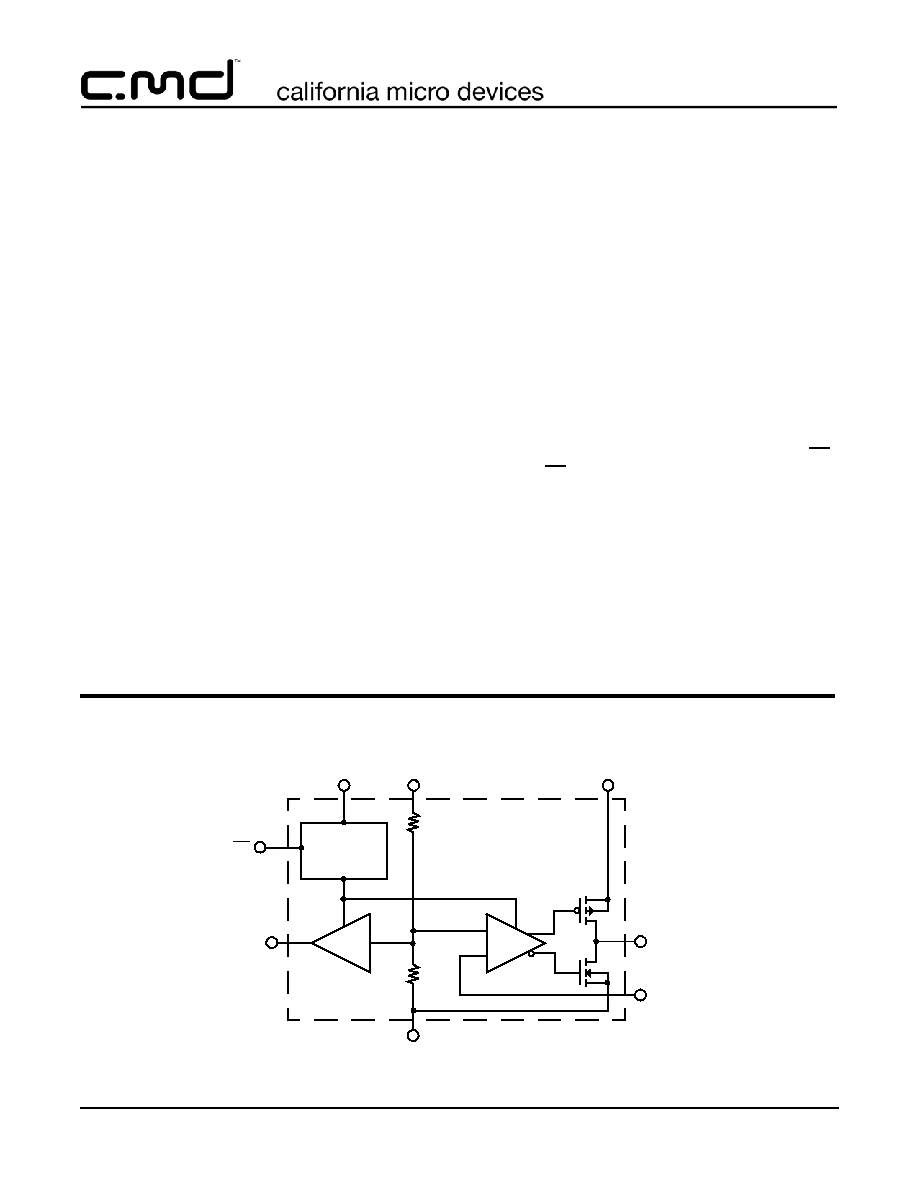
Simplified Electrical Schematic
V
REF
AV
IN
GND
V
SENSE
50K
IN
OUT
Buffer
V
TT
Driver
50K
V
DDQ
PV
IN
SD
Over Temp
Over Current
Reference
© 2004 California Micro Devices Corp. All rights reserved.
2
430 N. McCarthy Blvd., Milpitas, CA 95035-5112
Tel: 408.263.3214
Fax: 408.263.7846 www.calmicro.com
04/22/04
CM3196
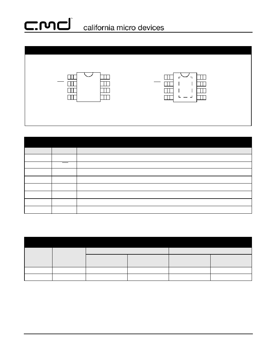
Ordering Information
Note 1: Parts are shipped in Tape & Reel form unless otherwise specified.
PIN DESCRIPTIONS
LEAD(S)
NAME
DESCRIPTION
1
GND
Ground
2
SD
Shutdown input, active low
3
V
SENSE
Feedback from V
TT
input
4
V
REF
Reference output, V
DDQ
/2
5
V
DDQ
V
DDQ
input
6
AV
IN
Analog circuit power input
7
PV
IN
Power transistor input
8
V
TT
Output
PACKAGE / PINOUT DIAGRAM
Note: This drawing is not to scale.
8-lead SOIC
1
2
3
4
8
7
6
5
GND
SD
V
SENSE
V
REF
V
TT
PV
IN
AV
IN
TOP VIEW
8-lead PSOP
1
2
3
4
8
7
6
5
GND
SD
V
SENSE
V
REF
V
TT
PV
IN
AV
IN
V
DDQ
TOP VIEW
GND
V
DDQ
PART NUMBERING INFORMATION
Pins
Package
Standard Finish
Lead-free Finish
Ordering Part
Number
1
Part Marking
Ordering Part
Number
1
Part Marking
8
SOIC-8
CM3196-12SN
CM3196-12SN
CM3196-12SM CM3196-12SM
8
PSOP-8
CM3196-12SB
CM3196-12SB
CM3196-12SH
CM3196-12SH
© 2004 California Micro Devices Corp. All rights reserved.
04/22/04
430 N. McCarthy Blvd., Milpitas, CA 95035-5112
Tel: 408.263.3214
Fax: 408.263.7846
www.calmicro.com
3
CM3196
Specifications
Note 1: These devices must be derated based on thermal resistance at elevated temperatures. The device packaged in an 8-pin
SOIC package must be derated at
JA
= 151
∞
C/W and the 8-pin PSOP must be derated at
JA
= 43
∞
C/W.
ABSOLUTE MAXIMUM RATINGS
PARAMETER
RATING
UNITS
AV
IN
Operating Supply Voltage
7
V
V
DDQ
Input Voltage
7
V
Pin Voltages
V
TT
Output
Any other pins
7
7
V
V
Storage Temperature Range
-40 to +150
∞C
Operating Temperature Range
Ambient
Junction
-40 to +85
-40 to +150
∞C
∞C
Power Dissipation (See note 1)
Internally Limited
W
© 2004 California Micro Devices Corp. All rights reserved.
4
430 N. McCarthy Blvd., Milpitas, CA 95035-5112
Tel: 408.263.3214
Fax: 408.263.7846 www.calmicro.com
04/22/04
CM3196
Specifications (cont'd)
DDR-I Features
Note 1: Operating characteristics are over Standard Operating Conditions unless otherwise specified.
STANDARD OPERATING CONDITIONS
PARAMETER
VALUE
UNITS
V
DDQ
2.5
V
AV
IN
2.5
V
PV
IN
2.5
V
Ambient Operating Temperature
-40 to +85
∞C
C
VOUT
220 +20%
µF
ELECTRICAL OPERATING CHARACTERISTICS
(SEE NOTE 1)
SYMBOL
PARAMETER
CONDITIONS
MIN
TYP
MAX
UNITS
V
IN
Input Voltage Range
PV
IN
pin
AV
IN
pin
2.2
2.2
2.5
2.5
AV
IN
5.5
V
V
I
CC
AV
IN
Quiescent Current
I
TT
= 0A
450
µA
I
CCSD
AV
IN
Quiescent Current
in Shut Down
V
SD
= logic "0"
115
µA
V
TT
V
TT
Output Voltage
PV
IN
= 2.5V
PV
IN
= 1.8V
PV
IN
= 1.5V
I
LOAD
= 0 to 2A or I
LOAD
= -2A to 0A
I
LOAD
= 0 to 0.75A or I
LOAD
= -0.75A to 0A
I
LOAD
= 0 to 0.3A or I
LOAD
= -0.3A to 0A
1.225
1.225
1.225
1.250
1.250
1.250
1.275
1.275
1.275
V
V
V
V
REF
Output Reference Voltage
V
DDQ
= 2.5V, I
REF
= 0A
1.225
1.250
1.275
V
VOS
VTT
Output Offset from V
REF
-30
30
mV
Z
REF
V
REF
Output Impedance
I
REF
= -5
µA to 5µA
5
k
Z
VDDQ
V
DDQ
Input Impedance
100
k
I
LIM
V
TT
Current Limit
2.5
A
V
SD
Shutdown Logic
Logic "1" Level
Logic "0" Level
1.5
0.4
V
V
T
DISABLE
T
HYST
Shutdown Temperature
Thermal Hysteresis
150
30
∞C
∞C
© 2004 California Micro Devices Corp. All rights reserved.
04/22/04
430 N. McCarthy Blvd., Milpitas, CA 95035-5112
Tel: 408.263.3214
Fax: 408.263.7846
www.calmicro.com
5
CM3196
Specifications (cont'd)
DDR-II Features
Note 1: Operating characteristics are over Standard Operating Conditions unless otherwise specified.
STANDARD OPERATING CONDITIONS
PARAMETER
VALUE
UNITS
V
DDQ
1.8
V
AV
IN
3.3
V
PV
IN
1.8
V
Ambient Operating Temperature
-40 to +85
∞C
C
VOUT
220 +20%
µF
ELECTRICAL OPERATING CHARACTERISTICS
(SEE NOTE 1)
SYMBOL
PARAMETER
CONDITIONS
MIN
TYP
MAX
UNITS
V
IN
Input Voltage Range
PV
IN
pin
AV
IN
pin
1.5
2.2
1.8
3.3
AV
IN
5.5
V
V
I
CC
AV
IN
Quiescent Current
I
TT
= 0A
450
µA
I
CCSD
AV
IN
Quiescent Current
in Shut Down
V
SD
= logic "0"
115
µA
V
TT
V
TT
Output Voltage
PV
IN
= 1.8V
PV
IN
= 1.5V
AV
IN
> 2.2V, PV
IN
>
2.2V
I
LOAD
= 0 to 0.6A or I
LOAD
= -0.6A to 0A
I
LOAD
= 0 to 0.3A or I
LOAD
= -0.3A to 0A
I
LOAD
= 0 to 1.2A or I
LOAD
= -1.2A to 0A
0.882
0.882
0.882
0.9
0.9
0.9
0.918
0.918
0.918
V
V
V
V
REF
Output Reference Voltage
V
DDQ
= 1.8V, I
REF
= 0A
0.882
0.9
0.918
V
VOS
VTT
Output Offset from V
REF
-30
30
mV
Z
REF
V
REF
Output Impedance
I
REF
= -5
µA to 5µA
5
k
Z
VDDQ
V
DDQ
Input Impedance
100
k
I
LIM
V
TT
Current Limit
2.5
A
V
SD
Shutdown Logic
Logic "1" Level
Logic "0" Level
1.5
0.4
V
V
T
DISABLE
T
HYST
Shutdown Temperature
Thermal Hysteresis
150
30
∞C
∞C