CALIFORNIA MICRO DEVICES
PRELIMINARY
CM3511
© 2002 California Micro Devices Corp. All rights reserved.
C0970500
11/10/03
430 N. McCarthy Blvd, Milpitas, California 95035 Tel: (408) 263-3214 Fax: (408) 263-7846 www.calmicro.com
1
Dual USB Overcurrent Switch 1.2A (V
CC
) / 200mA (V
SBY
)
Features
∑ Dual outputs, each with independent over-current
protection circuitry and indicator
∑ Supports standby mode in PCs so that a peripheral
can ramp down safely to a current <100mA
∑ Up
to
1.2A
(V
CC
) / 200mA (V
SBY
) continuous
current on each output
∑ Over-current limits at 1.2A / 200mA respectively
∑ 10msec min fault blanking delay on OC# outputs
prevents false overcurrent alarms
∑ Prevents backdrive current when host powered off
∑ Low operating current (95µA typ.)
∑ Small 8-Lead SOIC package
Applications
∑ PC motherboards, Notebooks, Set-Top-Boxes
The CM3511 also prevents backdrive current
flowing into the host from the connected peripheral.
This can occur when V
CC
is removed as the host
powers down, and the peripheral still has normal
power applied. The 5V from the peripheral can
therefore be linked to the host's V
BUS
, potentially
causing backdrive current into the host and
overloading the peripheral power supply.
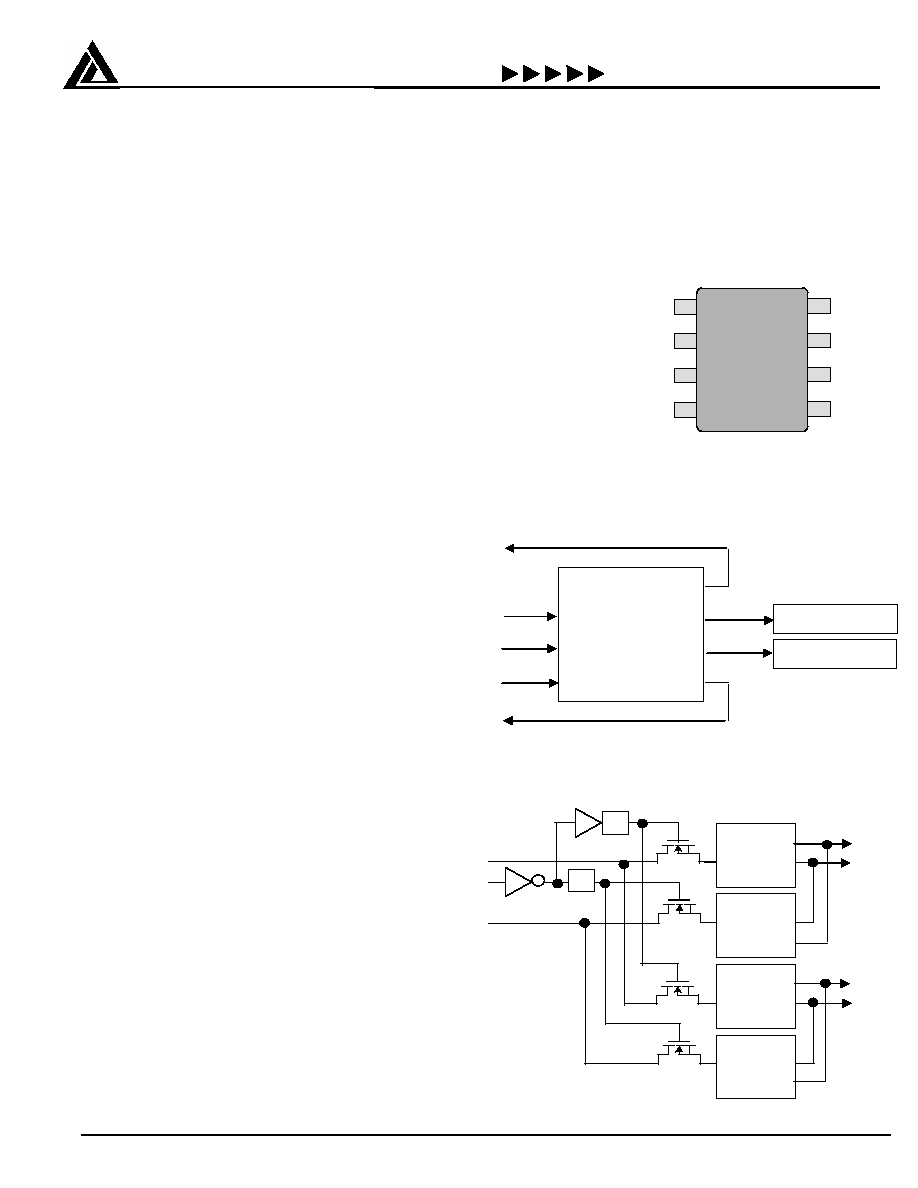
Pin Diagram
Product Description
California Micro Devices' CM3511 is a dual port
USB overcurrent power switch that selects between
two independent 5V inputs available on a PC,
depending on the state of a logic input (SEL). The
device has two pairs of power switches, and each
pair is an analog "OR" function, providing a
continuous voltage at both outputs during power
transfer between inputs.
V
CC
is the main 5V supply, which can be disabled in
a PC, and V
SBY
is the 5V standby supply which is
powered up whenever the PC has power. When the
`SEL' pin is at logic high, V
CC
is the assigned input
power supply. When `SEL' is at logic low, V
SBY
is
used to power the output, and no current is taken
from V
CC
. Both switches can be deselected and
switched off by not driving (floating) the `SEL' input,
which places the chip in low power mode.
Both pairs of switches have over-current protection.
Depending on whether `SEL' is high or low, a current
over 1.2A or 200mA respectively out of either output
causes the device to enter a constant-current mode,
where the output voltage is progressively reduced to
prevent the current from increasing further. Each
output is independent of the other, so if one of the
switches is switched on but is not in overcurrent
mode then it will remain switched on. The OC#
output becomes active only if the overcurrent
condition exceeds a minimum continuous duration of
10ms.
If the overcurrent condition is severe enough that
the part heats up to the thermal limit T
MAX
, the switch
turns off and the temperature cools down to T
MIN
.
The switch then turns on again, and the device
heats up again, and so on, until the fault is removed.
Typical Application Circuit
Simplified Electrical Schematic
OC1#
V
OUT1
OC2#
V
OUT2
V
CC
SEL
GND
V
SBY
SOIC-8
TOP
2 USB Ports
V
BUS
V
BUS
2 USB Ports
V
CC
SEL
GND
V
SBY
OC1#
V
OUT1
OC2#
V
OUT2
5V V
CC
5V V
SBY
Select V
CC
SEL
OC1#
V
OUT1
V
CC
H Over
current
protect
L Over
current
protect
OC2#
V
OUT2
V
SBY
H Over
current
protect
L Over
current
protect
CP
CP

CALIFORNIA MICRO DEVICES
PRELIMINARY
CM3511
© 2003 California Micro Devices Corp. All rights reserved
11/10/03
430 N. McCarthy Blvd, Milpitas, California 95035 Tel: (408) 263-3214 Fax: (408) 263-7846 www.calmicro.com
2
Absolute Maximum Ratings
Parameter
Rating
Unit
ESD Protection (All pins, HBM)
± 2000
V
V
CC
, V
SBY
Input Voltage
+ 5.6, GND - 0.5
V
Storage Temperature Range
Operating Ambient
Operating Junction
-55 to +150
-40 to +85
-40 to +150*
∞C
Output Current Loading
Internally limited
A
Package Power Dissipation
0.5
W
* - Internally limited
Operating Conditions
(unless specified otherwise)
Parameter
Range
Unit
V
CC
, V
SBY
Input Voltage
4.5 to 5.5
V
Ambient Temperature
-40 to +85
∞C
I
LOAD
per port
V
CC
V
SBY
0 to 1200
0 to 200
mA
Electrical Operating Characteristics
(over operating conditions unless specified otherwise)
Symbol Parameter
Conditions
MIN
TYP
MAX UNIT
UVLO V
CC
/V
SBY
voltage under which
circuit locks out - will not operate
2.2
2.5
V
V
OUT1
,
V
OUT2
Output Voltage
I
LOAD
= 1000mA, V
CC
= 5.0V,
SEL = 5V, T = 25
∞C
4.8 V
R
SW1
V
CC
Switch ON-Resistance
I
LOAD
= 0 to 1200mA; V
CC
= 5V
T=25
∞C
0.13
0.20
R
SW2
V
SBY
Switch ON-Resistance
I
LOAD
= 0 to 200mA; V
SBY
= 5V
T = 25
∞C
0.7
1.4
I
LIM VCC
V
CC
over-current limit
V
CC
= 5V SEL = high
1200
mA
I
LIM VSBY
V
SBY
over-current limit
V
SBY
= 5V SEL = low
200
mA
t
FBD
Time delay from overcurrent
detection to OC# output
indication (fault blanking delay)
10
20
ms
T
MAX
Temperature at which hot switch
turns off during overcurrent
150 ∞C
T
MIN
Temperature at which cool
switch turns on, after cooling
from T
MAX
125 ∞C
I
R CC
I
R SBY
Reverse leakage from outputs
to inputs ≠ backdrive current
V
CC
= 0V, V
OUT
= 5V, SEL floating
V
SBY
= 0V, V
OUT
= 5V, SEL floating
1
1
µA
I
CC ON
V
CC
operating supply current
95
µA
I
SBY OFF
V
SBY
standby supply current
V
CC
= 5V, V
SBY
< V
CC
, SEL = high,
I
LOAD
= 0mA
1 µA
I
SBY ON
V
SBY
operating supply current
95
µA
I
CC OFF
V
CC
standby supply current
V
SBY
= 5V, V
SBY
>V
CC
, SEL = low,
I
LOAD
= 0mA
1 µA
I
CC H Q
V
CC
higher, quiescent current
40
µA
I
SBY L Q
V
SBY
lower, quiescent current
V
CC
= 5V, V
SBY
< V
CC
, SEL floating
1 µA
I
CC L Q
V
CC
lower, quiescent current
1
µA
I
SBY H Q
V
SBY
higher, quiescent current
V
CC
= 5V, V
SBY
>V
CC
, SEL floating
40 µA
V
IH-EN
EN# input Logic-1 threshold
V
CC
= 5V
2 V
V
IL-EN
EN# input Logic-0 threshold
V
CC
= 5V
0.8
V
I
OHZ-OC
OC# output OFF state leakage
V
CC
= 5V, V
OUT
= 5V
1.0
uA
V
OL-OC
OC# output Logic-0 threshold
I
OC
= 1mA to V
CC
0.4
V
Note: the internal supply current is taken from whichever input (V
CC
or V
SBY
) is higher.
CALIFORNIA MICRO DEVICES
PRELIMINARY
CM3511
© 2003 California Micro Devices Corp. All rights reserved
11/10/03
430 N. McCarthy Blvd, Milpitas, California 95035 Tel: (408) 263-3214 Fax: (408) 263-7846 www.calmicro.com
3
Pin Functions
V
CC
is the higher current power source. Whenever the
SEL pin is above 2V it will be selected, and V
SBY
will be
deselected.
V
SBY
is the lower current power source. Whenever the
SEL pin is below 0.8V it will be selected, and V
CC
will
be deselected. The two V
SBY
power switches can only
supply 200mA each.
Note that the internal supply current (95uA typ.) will be
taken from whichever input supply pin (V
CC
or V
SBY
) is
higher.
V
SB
V
OUT1
provides the power for a USB port. The internal
MOSFET switches are designed for low voltage drops
from the voltage input pins at their full rated currents.
V
OUT2
provides the power for a second USB port. The
internal MOSFET switches are designed for low voltage
drops from the voltage input pins at their full rated
currents.
Current loads of up to 1.2A are allowed (sourced from
Vcc).
Current loads above 1.2A may cause the constant-
current limiting circuit to operate ≠ reducing the output
voltage.
Continuous over-current loads will cause the part's
internal temperature to rise. If the internal temperature
exceeds 150'C then any switch that is in overcurrent
mode will be immediately turned off. Any switch that is
not in overcurrent mode will remain on ≠ it will not be
affected by the over-temperature detection. Once the
part has cooled to 125'C then the switch or switches
that were in overcurrent mode will be automatically
turned on again.
During the cold-start interval when the input is initially
applied, internal circuitry provides a soft turn-on for
the switches, which limits peak in-rush current.
SEL
is the 3-level logic input pin that is used to
control which of the power switch pairs are turned on.
Set SEL high to select V
CC
, set SEL low to select
V
SBY
, or allow SEL to float to deselect both power
switches. The external device driving the SEL pin
must able to source and sink 100
µA while
maintaining the proper V
IL
/V
IH
levels.
OC1#, OC2#
are independent, active low open-
drain outputs, indicating an overcurrent fault condition
has been detected at V
OUT1
or V
OUT2
. There is a built-
in 10msec (min.) fault blanking period after the
overcurrent fault condition has been detected, before
these outputs become active. The OC# outputs
become deasserted only when both the overcurrent
condition stops and when the voltage drop across the
switch is less than 1V. External pull-up resistors of
10k - 100k are required if the OC# outputs are used.
Because they are open-drain, the two OC# outputs
can be shorted together to make one OC# signal.
GND
is the negative reference for all voltages.
Pin Functions
Pin No. Symbol Description
1
GND
Negative reference for all voltages.
2 V
CC
High current positive supply input.
3 V
SBY
Standby positive supply input. Also provides internal power.
4
SEL
3-level logic input. High = V
CC
, Low = V
SBY
, Floating = both off
5 OC2#
Active low when
V
OUT2
is in overcurrent mode.
6 V
OUT2
Output voltage internally switched to either V
CC
or V
SBY
input source.
7 V
OUT1
Output voltage internally switched to either V
CC
or V
SBY
input source.
8 OC1#
Active low when
V
OUT1
is in overcurrent mode.
STANDARD PART ORDERING INFORMATION
Pins
Package
Ordering Part Number
1
Part Marking
8 SOIC
CM3511-04SN
CM3511-04SN
CALIFORNIA MICRO DEVICES
PRELIMINARY
CM3511
© 2003 California Micro Devices Corp. All rights reserved
11/10/03
430 N. McCarthy Blvd, Milpitas, California 95035 Tel: (408) 263-3214 Fax: (408) 263-7846 www.calmicro.com
4
Note 1: Parts are shipped in Tape & Reel form unless otherwise specified.
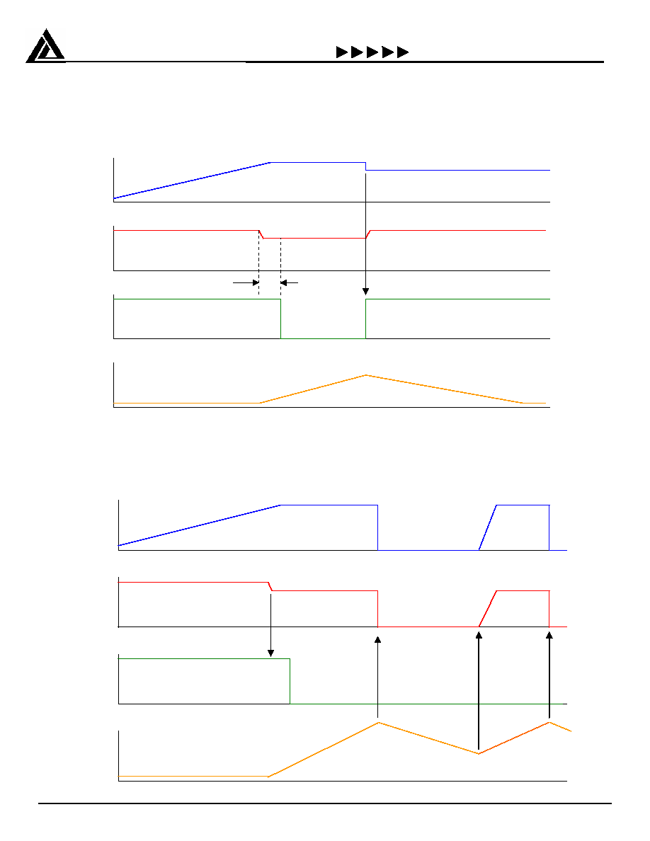
OC# Response to Momentary Overcurrent Fault
I
OUT
V
OUT
OC#
DieTemp.
>1200mA
<150'C
V
OUT
drops to reduce
I
OUT
OC# goes inactive as
soon
as overcurrent
condition stops
<1200mA
OC# goes active
after 10ms (min)
20ms (typ.) delay
I
OUT
V
OUT
OC#
Die Temp.
T
MAX
= 150'C
T
MIN
= 125'C
150'C
OC# Response to
Continuous Overcurrent Fault
V
OUT
drops to reduce I
OUT
Total powerdown when
over-temperature limit
reached
Re-powers when
temperature drops
to 125'C
OC# goes active
after 10ms (min)
20ms (typ.) delay
OC# stays low
Note: The other port stays on (unless it is also in current limit.)
>1200mA
CALIFORNIA MICRO DEVICES
PRELIMINARY
CM3511
© 2003 California Micro Devices Corp. All rights reserved
11/10/03
430 N. McCarthy Blvd, Milpitas, California 95035 Tel: (408) 263-3214 Fax: (408) 263-7846 www.calmicro.com
5
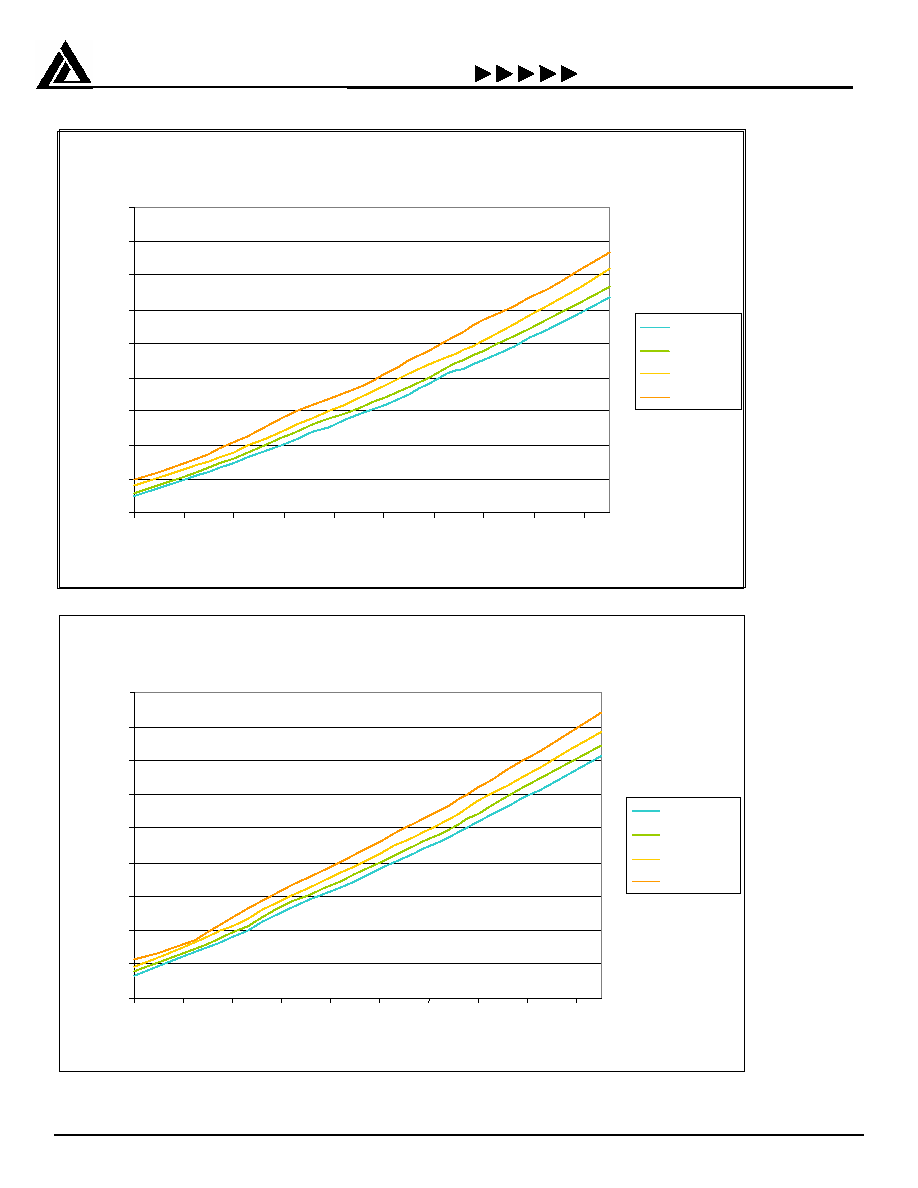
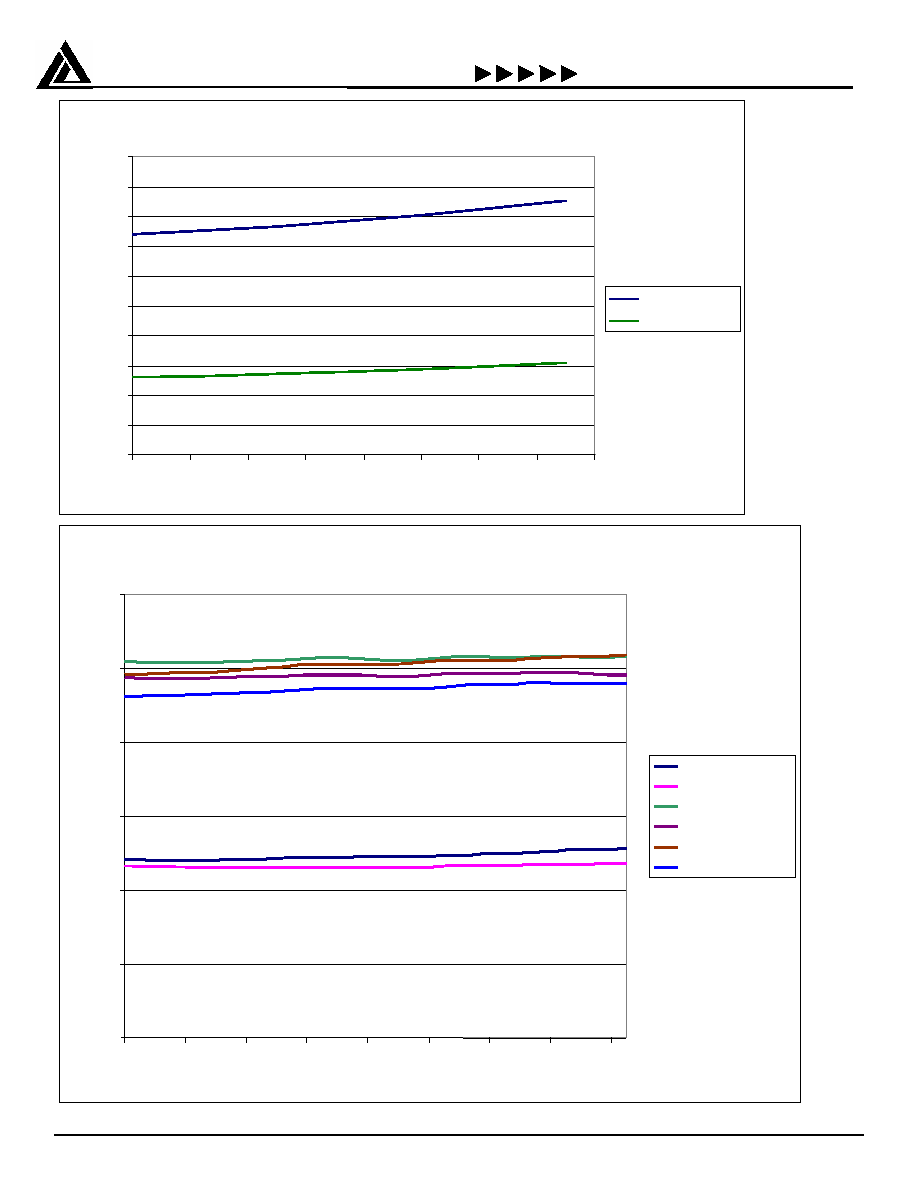
Typical Operating Characteristics
V
CC
On-resistance
100
110
120
130
140
150
160
170
180
190
-40
-20
0
20
40
60
80
100
120
140
Temperature ['C]
Resistance
[milliohms]
Vcc=5.5V
Vcc=5.0V
Vcc=4.5V
Vcc=4.0V
V
SBY
On-resistance
500
550
600
650
700
750
800
850
900
950
-40
-20
0
20
40
60
80
100
120
140
Temperature ['C]
Resistance
[milliohms]
Vsby=5.5V
Vsby=5.0V
Vsby=4.5V
Vsby=4.0V

CALIFORNIA MICRO DEVICES
PRELIMINARY
CM3511
© 2003 California Micro Devices Corp. All rights reserved
11/10/03
430 N. McCarthy Blvd, Milpitas, California 95035 Tel: (408) 263-3214 Fax: (408) 263-7846 www.calmicro.com
6
Vout-Iout characteristic (SEL=5V, Vcc active)
0
1
2
3
4
5
6
0
0.5
1
1.5
2
2.5
3
3.5
I
OU
[A]
V
OUT
[V]
Vout-Iout characteristic (SEL=0V, Vsby active)
0
1
2
3
4
5
6
0
0.1
0.2
0.3
0.4
0.5
0.6
I
OUT
[A]
V
OUT
[V]
CALIFORNIA MICRO DEVICES
PRELIMINARY
CM3511
© 2003 California Micro Devices Corp. All rights reserved
11/10/03
430 N. McCarthy Blvd, Milpitas, California 95035 Tel: (408) 263-3214 Fax: (408) 263-7846 www.calmicro.com
7
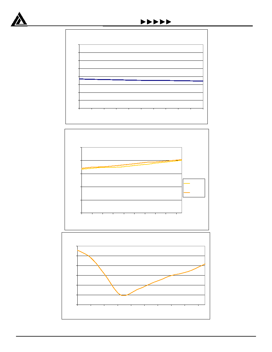
I
CC
vs. V
CC
20
30
40
50
60
70
80
90
100
110
120
4
4.2
4.4
4.6
4.8
5
5.2
5.4
5.6
V
CC
[V]
I
CC
[u
A
]
Idd(SEL=Vcc)
Idd(SEL=floats )
Supply current
0
20
40
60
80
100
120
-40
-20
0
20
40
60
80
100
120
Temperature ['C]
Current [uA]
Vcc=5.0V SEL=float
Vcc=4.0V SEL=float
Vcc=5.0V SEL=0V
Vcc=4.0V SEL=0V
Vcc=5.0V SEL=5V
Vcc=4.0V SEL=4V
CALIFORNIA MICRO DEVICES
PRELIMINARY
CM3511
© 2003 California Micro Devices Corp. All rights reserved
11/10/03
430 N. McCarthy Blvd, Milpitas, California 95035 Tel: (408) 263-3214 Fax: (408) 263-7846 www.calmicro.com
8
OC# Fault Blanking Period
0
5
10
15
20
25
30
35
40
3.5
3.7
3.9
4.1
4.3
4.5
4.7
4.9
5.1
5.3
5.5
V
CC
[V]
D
e
l
ay [
m
se
c]
OC# Fault Blanking Period
0
5
10
15
20
25
-40
-20
0
20
40
60
80
100
120
140
Temperature ['C]
T
i
m
e
[
m
il
li
seco
n
d
s]
Vcc=5.0V
Vcc=4.0V
Undervoltage Lock-Out (UVLO)
1.95
2
2.05
2.1
2.15
2.2
2.25
-40
-20
0
20
40
60
80
100
120
140
Tem perature ['C]
S
u
p
p
ly
v
o
lt
a
g
e
V
CC
or
V
SB
Y
[V
]

CALIFORNIA MICRO DEVICES
PRELIMINARY
CM3511
© 2003 California Micro Devices Corp. All rights reserved
11/10/03
430 N. McCarthy Blvd, Milpitas, California 95035 Tel: (408) 263-3214 Fax: (408) 263-7846 www.calmicro.com
9
V
CC
Turn-on time
0
50
100
150
200
250
-40
-20
0
20
40
60
80
Tempe rature ['C]
T
i
m
e
[u
sec]
Vcc=5.5V
Vcc=4.5V
V
SBY
Turn-on time
0
1
2
3
4
5
-40
-20
0
20
40
60
80
Temperature ['C]
T
i
m
e
[
u
sec]
Vsby=5.5V
Vsby=4.5V
V
CC
Turn-off time
0.0
1.0
2.0
3.0
4.0
5.0
-40
-20
0
20
40
60
80
Te mpe rature ['C]
T
i
m
e
[u
sec]
Vcc=5.5V
Vcc=4.5V

CALIFORNIA MICRO DEVICES
PRELIMINARY
CM3511
© 2003 California Micro Devices Corp. All rights reserved
11/10/03
430 N. McCarthy Blvd, Milpitas, California 95035 Tel: (408) 263-3214 Fax: (408) 263-7846 www.calmicro.com
10
V
SBY
Turn-off time
0
10
20
30
40
50
-40
-20
0
20
40
60
80
Temperature ['C]
T
i
m
e
[
u
sec]
Vsby=5.5V
Vsby=4.5V
Turn-on time v s. V
CC
0
20
40
60
80
100
120
140
160
180
4
4.5
5
5.5
V
CC
[V]
T
i
m
e
[
u
sec]
Cout=0.1u
Cout=1u
Turn-on time v s. V
SBY
0
0.5
1
1.5
2
2.5
3
3.5
4
4.5
5
4
4.5
5
5.5
V
SBY
[V]
T
i
m
e
[
u
sec]
Cout=0.1u
Cout=1u

CALIFORNIA MICRO DEVICES
PRELIMINARY
CM3511
© 2003 California Micro Devices Corp. All rights reserved
11/10/03
430 N. McCarthy Blvd, Milpitas, California 95035 Tel: (408) 263-3214 Fax: (408) 263-7846 www.calmicro.com
11
Turn-off time vs. V
C C
0
5
10
15
20
25
30
4
4.5
5
5.5
V
CC
[V]
T
i
m
e
[
u
sec
]
Cout=0.1u
Cout=1u
Turn-off time vs. V
SB Y
0
50
100
150
200
250
300
4
4.5
5
5.5
V
SBY
[V]
T
i
m
e
[
u
s
ec]
Cout=0.1u
Cout=1u
CALIFORNIA MICRO DEVICES
PRELIMINARY
CM3511
© 2003 California Micro Devices Corp. All rights reserved
11/10/03
430 N. McCarthy Blvd, Milpitas, California 95035 Tel: (408) 263-3214 Fax: (408) 263-7846 www.calmicro.com
12
Normalized Overcurrent indicator trip point (V
CC
)
0.50
0.60
0.70
0.80
0.90
1.00
1.10
1.20
1.30
1.40
1.50
-40
-20
0
20
40
60
80
100
120
Temperature ['C]
C
u
r
r
e
nt
[
nor
m
a
liz
e
d
]
Vcc=5.5V
Vcc=4.5V
Normalized Overcurrent indicator trip point (V
SBY
)
0.80
0.85
0.90
0.95
1.00
1.05
1.10
1.15
1.20
-40
-20
0
20
40
60
80
100
120
Temperature ['C]
C
u
r
r
e
n
t [n
o
r
m
a
l
i
z
e
d
]
Vsby=5.5V
Vsby=4.5V
CALIFORNIA MICRO DEVICES
PRELIMINARY
CM3511
© 2003 California Micro Devices Corp. All rights reserved
11/10/03
430 N. McCarthy Blvd, Milpitas, California 95035 Tel: (408) 263-3214 Fax: (408) 263-7846 www.calmicro.com
13
SOIC-8 Package Dimensions