
CALIFORNIA MICRO DEVICES
PRELIMINARY
CM3702
© 2004 California Micro Devices Corp. All rights reserved.
9/22/04 430 N. McCarthy Blvd, #100, Milpitas , CA 95035 Tel: (408) 263-3214 Fax: (408) 263-7846 www.calmicro.com
1
Micropower Low-Noise Charge-Pump and Linear Regulator
Features
∑ Low noise regulator with integrated charge
pump voltage-booster
∑ 5V output with input voltage as low as 2.8V
∑ Charge pump can also power external LDO
∑ Low noise in 20Hz to 20kHz audio band
∑ Up to 200mA continuous output current
∑ Low operating and shutdown currents
∑ Stable with low-ESR ceramic or tantalum
capacitors
∑ 10-Lead MSOP and TDFN packages
∑ Lead-free
finishing
Applications
∑ 5V analog supply for audio codec in notebook
computers, PDAs, MP3 players, etc.
∑ 3.3V to 5V conversion in PCMCIA cards, PCI
Express Cards, other applications needing 5V
Block Diagram
Product Description
The CM3702 low-noise charge pump LDO regulator is designed to provide accurate and "clean" power to a
subsystem, e.g an audio codec, LED driver, or flash memory. The 5V output provides up to 100mA continuous
current for input voltages from 2.8V to 5.5V, and up to 200mA for a narrower range. This is accomplished with an
integrated charge pump that boosts the input voltage before feeding it to an internal LDO linear regulator. The
charge pump is designed to maintain a nominal 0.8V differential between the input and output of the LDO
regulator. This allows the LDO regulator to operate with good power supply ripple rejection across the audio band
while maintaining good power efficiency. The charge pump works with two external capacitors and operates at
250kHz, well outside the audible frequency band. In addition, separate analog and digital ground pins are
provided for the charge pump and the rest of the circuitry to eliminate ground noise feed-through from the charge
pump to the regulated output.
The CM3702 is fully protected, offering both overload current limiting and high temperature thermal shutdown.
Two enable inputs provide flexibility in powering down the device. For maximum power saving in shutdown, both
the charge pump and LDO regulator should be disabled. For applications that require the 5V output to be re-
established with minimum delay after shutdown, the charge pump can be left enabled while the regulator is
disabled. This avoids the delay that may otherwise be required for the charge pump to reach full operating
voltage after being disabled. The CMOS LDO regulator features low quiescent current even at full load, making it
very suitable for power sensitive applications.
A bandgap reference bypass pin is provided to further minimize noise by connecting an external capacitor
between this pin and ground. Another, external, regulator can be connected to the charge pump output pin Cs, if
required.
The CM3702 is available in 10-pin MSOP and TDFN packages, both with optional lead-free finishing, and are
ideal for space critical applications.
STANDARD PART ORDERING INFORMATION
Standard Finish
Lead-free Finish
Pins Package
Ordering Part
Number Part
Marking
Ordering Part
Number Part
Marking
10
MSOP-10
CM3702-50MR
3702 50S
CM3702-50MS
3702 50
10
TDFN-10
CM3702-50DF
CM370 250DF
CM3702-50DE
CM370 250DE
CALIFORNIA MICRO DEVICES
PRELIMINARY
CM3702
© 2004 California Micro Devices Corp. All rights reserved
09/22/04
430 N. McCarthy Blvd, #100, Milpitas, California 95035 Tel: (408) 263-3214 Fax: (408) 263-7846 www.calmicro.com
2
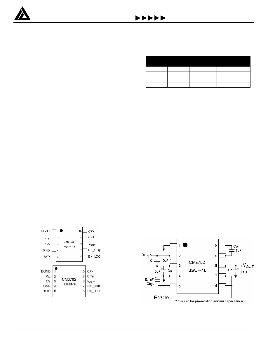
Pin Descriptions
V
IN
(pin 2) is the input power source for the device. Since
the charge pump draws current in pulses at the 250kHz
internal clock frequency, a low-ESR input decoupling
capacitor is usually required close to this pin to ensure
low noise operation.
CP+
and
CP-
(pins 9, 10) are used to connect the
external "flying" capacitor C
P
to the charge pump. The
charge stored in C
P
is transferred to the reservoir
capacitor C
S
at the 250kHz internal clock rate.
CS
(pin 3) is the output of the charge pump and is
connected to the external reservoir capacitor Cs. This
should be a low-ESR capacitor.
When the voltage on this pin reaches about 5.8V then
the charge pump pauses until the voltage on this pin
drops to about 5.7V. This gives rise to at least 100mV of
`ripple' (the frequency and amplitude of this ripple
depends upon values of Cp and Cs and also the ESR of
Cs).
Note that current may be drawn from this pin for other
applications (for example an additional, independent, 5V
LDO) as long as the total current is less than 100mA
(otherwise the part may overheat).
DGND
(pin 1)
is the ground for the charge pump circuit.
This should be connected to the system (noisy) ground.
GND
(pin 4) is the ground reference for all internal circuits
except the charge pump. This pin should be connected to
a "clean" low-noise analog ground.
EN_LDO, EN_Chip
(pins 6, 7) are active-high TTL-level
logic inputs to enable the linear regulator and charge
pump according to the following truth table:
EN_Chip
Pin 7
EN_LDO
Pin 6
CHARGE
PUMP
REGULATOR
1 1
Enabled
Enabled
1 0
Enabled
Disabled
0 1
Disabled
Disabled
0 0
Disabled
Disabled
When the LDO Regulator is disabled, an internal pull-
down with a nominal resistance of 500
is activated to
discharge the 5V output rail to ground.
When the charge pump is disabled or paused, the
internal 250kHz oscillator is disabled. The "flying
capacitor" C
P
will then stay connected between V_IN
and DGND, and C
S
will stay connected to the input of
the LDO regulator. In this mode, C
S
will discharge at a
rate determined by the input current of the LDO regulator.
BYP
(pin 5) is connected to the internal voltage reference
of the LDO regulator. An external bypass capacitor C
BYP
of 0.1uF is recommended to minimize internal voltage
reference noise and maximize power supply ripple
rejection.
V
OUT
(pin 8) is the regulated output. An output capacitor
may be added to improve noise and load-transient
response. When the LDO regulator is disabled, an internal
pull-down is activated to discharge the V
OUT
rail to GND.
Pinout Diagrams
Typical Application Circuit

CALIFORNIA MICRO DEVICES
PRELIMINARY
CM3702
© 2004 California Micro Devices Corp. All rights reserved
09/22/04
430 N. McCarthy Blvd, #100, Milpitas, California 95035 Tel: (408) 263-3214 Fax: (408) 263-7846 www.calmicro.com
3
Absolute Maximum Ratings
Parameter
Rating
Unit
ESD Protection (HBM)
2000
V
V
IN
, V
OUT
Voltages
+ 5.5, Gnd - 0.5
V
V
EN
Logic Input Voltage
V
IN
+ 0.5, Gnd - 0.5
V
Temperature: Storage
Operating Ambient
Operating Junction
-40 to +150
0 to +70
0 to +170
∞C
Standard Operating Conditions
Parameter
Range
Unit
V
IN
- Input Voltage Range
3.0 to 5.5
V
Ambient Operating Temperature
0 to +70
∞C
JA
of MSOP package on pcb
200 (approx)
∞C/W
I
OUT
- Output Load Current
0 to 200
mA
C
BYP
0.1
µF
C
OUT
0
to
100
µF
Electrical Operating Characteristics
(V
IN
= 5.0V; I
OUT
=100mA; C
OUT
=10uF; C
P
= 1
µF; C
S
= 10
µF;
unless specified otherwise)
Symbol Parameter
Conditions
MIN
TYP
MAX
UNIT
V
CS
Charge pump output voltage
V
OUT
= 5V, 1mA
I
OUT
100mA;
5.5 5.8 7 V
V
OUT
Regulator Output Voltage
V
IN
= 4.0V; 1mA
I
OUT
100mA;
4.85 5.15 V
V
R LOAD
Load
Regulation
I
OUT
= 1mA to 100mA
0.2
%
V
R LINE
Line Regulation
Vary V
IN
from 3.0V to 5.0V
0.02
%
R
DISCHG
V
OUT
Discharge Resistance
LDO regulator disabled
EN2 (pin 6) grounded; V
IN
= 5V
500
Shutdown (EN2 grounded)
1
10
µA
Regulator Enabled, I
OUT
=
0mA
180
µA
I
GND
LDO Regulator Ground Current via
GND pin
Regulator Enabled, I
OUT
= 100mA
180
µA
I
DGND
Charge Pump Shutdown Current
via DGND pin
EN1 (pin 7) grounded, V
IN
= 5.0V
1
10
µA
PSRR
Power Supply Rejection
I
OUT
= 100mA; C
BYP
=0.1uF
f = 100Hz
f = 10kHz
42
42
dB
dB
e
NO
Output Voltage Noise
BW=22Hz-22kHz; C
OUT
=10uF;
C
BYP
=0.1uF; I
OUT
= 100mA
35
µVrms
e
NO
Output Voltage Noise
BW=22Hz-22kHz; C
p
=1uF, C
S
=3uF
C
OUT
=C
BYP
=0.1uF; I
OUT
= 100mA
38
µVrms
V
IH
EN1, EN2 Input High threshold
V
IN
= 5.0V
2.0
V
V
IL
EN1, EN2 Input Low threshold
V
IN
= 5.0V
0.5
V
I
LIM
Overload Current Limit
(LDO only)
200
300
mA
I
SC
Output Short Circuit Current
(LDO only)
100
200
mA
T
JSD
Thermal Shutdown Junction Temp
170
∞C
T
HYS
Thermal Shutdown Hysteresis
25
∞C

CALIFORNIA MICRO DEVICES
PRELIMINARY
CM3702
© 2004 California Micro Devices Corp. All rights reserved
09/22/04
430 N. McCarthy Blvd, #100, Milpitas, California 95035 Tel: (408) 263-3214 Fax: (408) 263-7846 www.calmicro.com
4
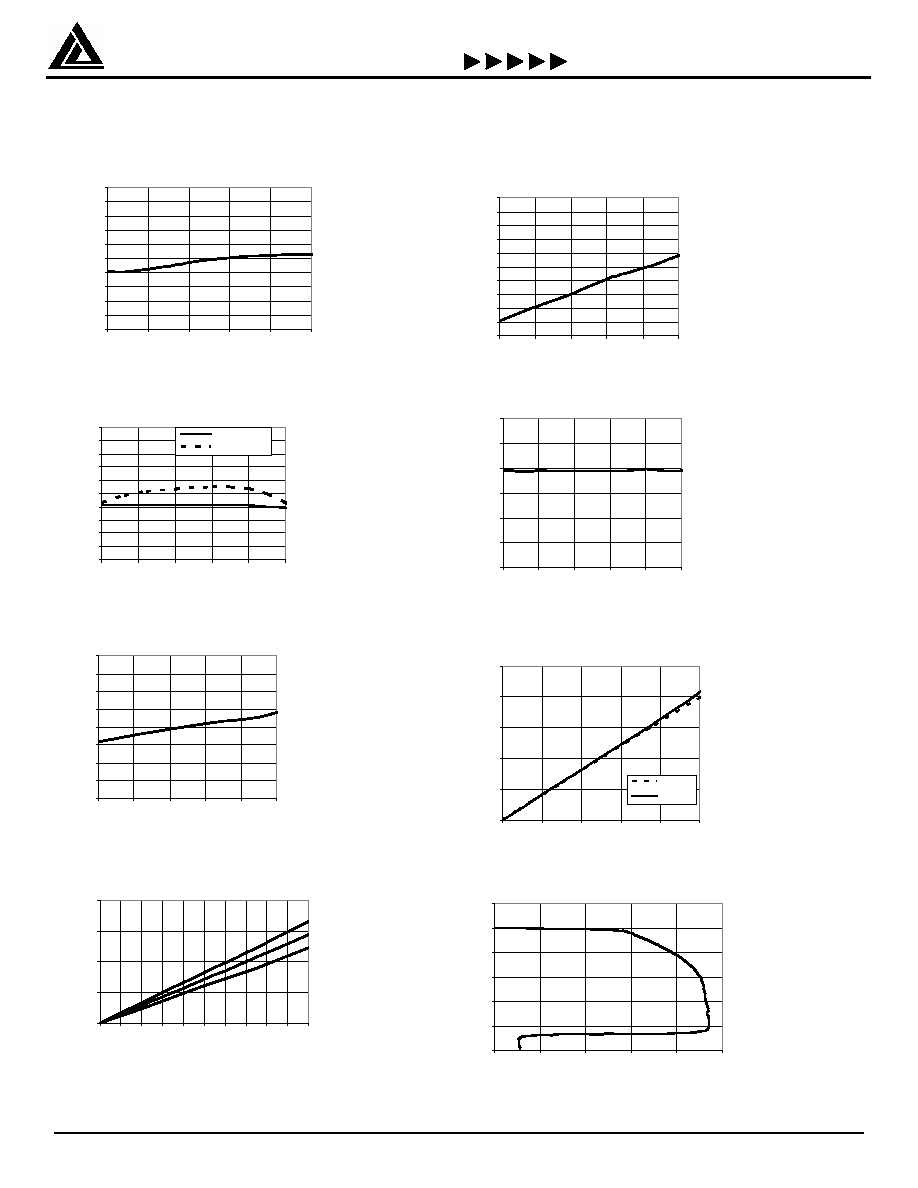
Typical Performance Characteristics
(T=25
∞C)
CM3702 noise spectrum
(Cp=0.47uF, Cs=1.5uF, Co=Cbyp=0.1uF, Iout=100mA)
1.00E-08
1.00E-07
1.00E-06
1.00E-05
1.00E-04
1.00E-03
10
100
1000
10000
100000
Frequency [Hz]
V
o
l
t
ag
e [
V
]
noise floor
Cs=1.5uF
Note: Noise peaks may appear for different values of Cp, Cs & I
OUT
, and are due to the ripple frequency of the charge pump (see
later).
Measured by forcing V
IN
voltage to 3.3V & 5.0V dc, then sweeping 100mV ac on V
IN
. C
OUT
= 10uF, C
BYP
= 0.1uF
PSRR with V
IN
=3.3V (upper curve) and V
IN
=5V (lower curve), I
OUT
=100mA
0.0
10.0
20.0
30.0
40.0
50.0
60.0
70.0
10
100
1000
10000
100000
Frequency [Hz]
P
S
RR [dB]
CALIFORNIA MICRO DEVICES
PRELIMINARY
CM3702
© 2004 California Micro Devices Corp. All rights reserved
09/22/04
430 N. McCarthy Blvd, #100, Milpitas, California 95035 Tel: (408) 263-3214 Fax: (408) 263-7846 www.calmicro.com
5
Typical Performance Characteristics
(T=25
∞C, Cp=1uF, Cs=10uF, Cbyp=0.1uF, C_OUT=10uF unless stated)
V_OUT v s. I_OUT
(V_IN = 5V)
4.9
4.92
4.94
4.96
4.98
5
5.02
5.04
5.06
5.08
5.1
0
20
40
60
80
100
I_OUT [mA]
V_
O
U
T
[
V
]
V_OUT vs. V_IN
4.9
4.92
4.94
4.96
4.98
5
5.02
5.04
5.06
5.08
5.1
3
3.5
4
4.5
5
5.5
V_IN [V]
V_
O
U
T
[
V
]
I_OUT=0mA
I_OUT=100mA
CS pin vs. V_IN
5
5.25
5.5
5.75
6
6.25
6.5
6.75
7
3
3.5
4
4.5
5
5.5
V_IN [V]
C
S
pi
n [
V
]
V_EN Threshold vs. V_IN
1
1.1
1.2
1.3
1.4
1.5
1.6
1.7
1.8
1.9
2
3
3.5
4
4.5
5
5.5
V_IN [V]
V_
EN
[
V
]
I_IN vs. V_IN
0
50
100
150
200
250
300
3
3.5
4
4.5
5
5.5
V_IN [V]
I_
IN
[
u
A
]
I_IN vs. I_OUT
0
50
100
150
200
250
0
20
40
60
80
100
I_OUT [mA]
I
_
IN
[
m
A
]
V_IN=3.1V
V_IN=5V
Overcurrent characteristic (LDO only)
0
1
2
3
4
5
6
0
0.1
0.2
0.3
0.4
0.5
I_OUT [A]
V_
O
U
T
[
V
]
DROPOUT VOLTAGE
(LDO ONLY)
at T=150'C, T=85'C and T=25'C
0
100
200
300
400
0
10
20
30
40
50
60
70
80
90 100
I_OUT [mA]
V
DO
[m
V]