
PRELIMINARY
CM9107
Triple-Output LDO for WLAN
Features
∑
3.0V to 3.6V input voltage range
∑
Preset output voltage with excellent line and load
regulation
∑
LDO1 = 1.80V/500mA, ±1.5% max load regulation
∑
LDO2 = 2.84V/300mA, ±1% max load regulation
∑
LDO3 = 2.84V/200mA, ±1% max load regulation
∑
Low output noise (<30µVrms for LDO3)
∑
Low dropout voltage; 135mV (typ.) for LDO2 at
300mA, and 110mV (typ.) for LDO3 at 200mA.
∑
Low quiescent current, < 600µA typical
∑
Integrated microprocessor RESET circuit with
adjustable RESET delay (2.5ms per nF of C
T
)
∑
Logic controlled shutdown
∑
Power good signal
∑
Built-in power up and power down sequence con
trol between LDO1 and LDO2
∑
Over-temperature and over-current protection
∑
TQFN-16, RoHS compliant lead-free package
Applications
∑
Wireless LAN 802.11 chipset power supply
∑
Wireless LAN cards
∑
Wireless instrumentation
Product Description
The CM9107 is a triple-output, low noise, low dropout
(LDO) linear regulator with an integrated microproces
sor reset circuit. It is designed for use with wireless
local-area network chipsets. It has an input voltage
range of 3.0V to 3.6V, and supplies a 500mA, 1.80V
preset output (LDO1); a 300mA, 2.84V output (LDO2),
and a 200mA, low noise output of 2.84V (LDO3). The
CM9107 has excellent line and load regulation over the
operating temperature range.
The CM9107 LDOs features low dropout voltage by
using efficient P-channel MOSFETs for each output. It
also features a power good signal (active high) when
all three LDOs are in regulation. It provides two shut
down control pins, LDO1 and LDO2 power sequencing,
plus short-circuit and over-temperature shutdown pro
tection.
The CM9107 also provides a microprocessor RESET
circuit with RST and RST outputs. The RESET signal
is asserted when the V
IN
supply voltage drops below
2.63V, remaining asserted for the adjustable RESET
delay period, controlled by an external capacitor on the
CT pin.
The CM9107 is packaged in a 16-pin TQFN (4mm x
4mm) package. It can operate over the industrial tem
perature range of ≠40∞C to 85∞C.
Typical Application
3.0V to 3.6V
10uF
C
IN
16
15
13
12
1.8V, 500mA
Baseband
1
CT
SHDN
VO
3
SHDN3
CM9107
CC3
GN
D
3
GN
D
CB1
VO1
VO2
CC2
RS
T
PG
O
O
D
VI
N
3
VI
N
RST
14
Processor/
MAC
C
o1
3.3uF
11
2
0.01uF
10
2.84V, 300mA
C
T
Analog
3
Circuitry
C
o2
3.3uF
4
9
C
b
0.033uF
5
6
7
8
2.84V, 200mA
VCO
C
o3
3.3uF
©
2006 California Micro Devices Corp. All rights reserved.
07/11/06
490 N. McCarthy Blvd., Milpitas, CA 95035-5112
l
Tel: 408.263.3214
l
Fax: 408.263.7846
l
www.cmd.com
1

PRELIMINARY
CM9107
Package Pinout
PACKAGE / PINOUT DIAGRAM
CM9107-00QE
4
3
2
1
9
10
11
12
5
6
7
8
16
15
14
13
GND
PAD
BOTTOM VIEW
(Pins Up View)
TOP VIEW
(Pins Down View)
SHDN3
SHDN
CT
RST
CC2
VO2
CB1
VO1
RS
T
PGOOD
VI
N
3
VI
N
VO
3
CC
3
GND
3
GN
D
4
3
2
1
9
10
11
12
5
6
7
8
16
15
14
13
CM9
1
0
70
0Q
E
Pin 1
Marking
16-Lead TQFN Package (4mmx4mm)
Note: This drawing is not to scale.
PIN DESCRIPTIONS
LEAD(s)
NAME
DESCRIPTION
1
RST
Reset bar pin. This is the inverse output of the RST signal pin (pin 16).
2
CT
CT pin for setting the delay time for RST assert (2.5ms per nF).
3
SHDN
Shutdown control input pin for LDO1 and LDO2. Active low, LDO1 and LDO2 will be off when
the pin is pulled low. Connect to V
IN
when unused.
4
SHDN3
Shutdown control input pin for LDO3. Active low. Connect to V
IN
when unused.
5
VO3
LDO3 output pin (2.84V). Connect a low-ESR bypass capacitor of 2.2µF, minimum.
6
CC3
This pin is used for testing. In the application it could be either floating or tied to ground
7
GND3
Ground pin for LDO3
8
GND
Ground pin for LDO1, LDO2 and control circuit
9
CC2
This pin is used for testing. In the application it could be either floating or tied to ground
10
VO2
LDO2 output pin (2.84V). Connect a low-ESR bypass capacitor of 2.2µF, minimum.
11
CB1
Bypass capacitor pin for internal bandgap reference (typically 0.033µF low-ESR type).
12
VO1
LDO1 output pin (1.80V). Connect a low-ESR bypass capacitor of 2.2µF, minimum.
13
VIN
Power input pin for LDO2 and LDO3. Connect to a low-ESR bypass capacitor of 2.2µF,
minimum.
14
VIN3
Power input pin for LDO3. Connect to Pin 13, on the PC board, very near the device.
15
PGOOD
Power good output pin with internal pull-up resistor to VIN, goes high when all 3 LDOs are in
regulation.
©
2006 California Micro Devices Corp. All rights reserved.
2
490 N. McCarthy Blvd., Milpitas, CA 95035-5112
l
Tel: 408.263.3214
l
Fax: 408.263.7846
l
www.cmd.com
07/11/06
PRELIMINARY
CM9107
Pin Descriptions (cont'd)
16
RST
Reset output pin. When V
IN
falls below the RESET threshold, this RST pin is asserted (active
high). When V
IN
rises above the RESET threshold, RST goes low after a delay of 2.5ms per
nF of CT capacitance. Refer to RESET section in the Application Information.
PIN DESCRIPTIONS
Ordering Information
PART NUMBERING INFORMATION
Pins
Package
Lead Free Finish
Ordering Part Number
1
Part Marking
16
TQFN
CM9107-00QE
CM9107 00QE
Note 1: Parts are shipped in Tape & Reel form unless otherwise specified.
Specifications
ABSOLUTE MAXIMUM RATINGS
PARAMETER
RATING
UNITS
ESD Protection (HBM)
±2
kV
V
IN
, V
IN3
, GND3 to GND
[GND - 0.3] to +6.0
V
Pin Voltages
V
O1
, V
O2
, V
O3
to GND
C
B1
to GND to GND
SHDN, SHDN3 to GND
CT, RST, RST, PGOOD to GND
[GND - 0.3] to +6.0
[GND - 0.3] to +6.0
[GND - 0.3] to +5.0
[GND - 0.3] to +5.0
V
V
V
V
Storage Temperature Range
-65 to +150
∞C
Operating Temperature Range (Ambient)
-40 to +85
∞C
Lead Temperature (Soldering, 10sec)
300
∞C
ELECTRICAL OPERATING CHARACTERISTICS
(SEE NOTE 1)
SYMBOL
PARAMETER
CONDITIONS
MIN
TYP
MAX
UNITS
V
IN
Input Supply Voltage
3.0
3.3
3.6
V
I
Q
Quiescent Current
All outputs are no load
600
750
µA
V
SHDN
Shutdown Supply Current
SHDN = SHDN3 = 0
5.0
10
µA
V
IL
Shutdown (active low) Input
Low Threshold
0.4
V
V
IH
Shutdown Input High Threshold
2.0
V
T
START
Start-up Time (from SHDN
going high to V
OUT
in
regulation) (Note 3)
V
OUT
= 95% of final value
120
µs
©
2006 California Micro Devices Corp. All rights reserved.
07/11/06
490 N. McCarthy Blvd., Milpitas, CA 95035-5112
l
Tel: 408.263.3214
l
Fax: 408.263.7846
l
www.cmd.com
3
PRELIMINARY
CM9107
Specifications (cont'd)
ELECTRICAL OPERATING CHARACTERISTICS
(SEE NOTE 1)
SYMBOL
PARAMETER
CONDITIONS
MIN
TYP
MAX
UNITS
T
PGOOD
PGOOD Threshold
All output currents = 50% rating
-5
+5
%
O
PGOOD
PGOOD Output Level
I
SINK
= 2mA
0.25
V
T
OVER
OTP Threshold
150
∫C
T
HYS
OTP Hysteresis
20
∫C
UVLO
Undervoltage Lockout (Note 2)
All outputs are no load.
2.20
2.45
2.65
V
LDO1
V
OUT
Output Voltage
1.80
V
V
OUT acc
Output Voltage Accuracy
I
OUT
= 10mA
-1.5
+1.5
%
I
LIM
Over-current Limit (Note 2)
550
750
mA
V
R LIN
Line Regulation
V
IN
= 3.0V to 3.6V, I
OUT
= 10mA
-0.15
0.15
%/V
V
R LOAD
Load Regulation (Note 5)
I
OUT
=10mA to 500mA
-1.5
1.5
%
V
OUT N
Output Noise
10Hz < f < 100kHz, Co1 = 3.3µF,
I
OUT
= 50mA
100
µVrms
LDO2
V
OUT
Output Voltage
2.84
V
V
OUT acc
Output Voltage Accuracy
I
OUT
= 10mA
-1.5
+1.5
%
I
LIM
Over-current Limit (Note 2)
330
550
mA
V
R LIN
Line Regulation
V
IN
= 3.0V to 3.6V, I
OUT
= 10mA
-0.15
0.15
%/V
V
R LOAD
Load Regulation (Note 5)
I
OUT
= 10mA to 300mA
0.2
1.0
%
V
DROP
Dropout Voltage (Note 4)
I
OUT
= 30 mA
135
220
mV
V
OUT N
Output Noise
10Hz < f < 100kHz, I
OUT
= 10mA
Co2 = 2.2µF
Co2 = 10µF
70
60
µVrms
µVrms
LDO3
V
OUT
Output Voltage
2.84
V
V
OUT acc
Output Voltage Accuracy
I
OUT
= 10mA
-1.5
+1.5
%
I
LIM
Over-current Limit (Note 2)
250
450
mA
V
R LIN
Line Regulation
V
IN3
= 3.0V to 3.6V, I
OUT
= 10mA
-0.15
0.15
%/V
V
R LOAD
Load Regulation (Note 5)
I
OUT
= 10mA to 200mA
0.2
1.0
%
V
DROP
Dropout Voltage (Note 4)
I
OUT
= 200mA
110
200
mV
V
OUT N
Output Noise
10Hz < f < 100kHz, I
OUT
= 10mA
Co3 = 2.2µF
Co3 = 10µF
30
20
µVrms
µVrms
RESET
T
RESET
RESET Threshold (Vth) (Note
2)
2.56
2.63
2.69
V
T
HYS RESET
RESET Threshold Hysteresis
10
mV
V
DROP RESETD
V
IN
Dropout Reset Delay
V
CC
= Vth to Vth ≠100mV
20
µs
T
RST
RST / RST Timeout Period
(Note 2)
CT = 10nF
25
ms
©
2006 California Micro Devices Corp. All rights reserved.
4
490 N. McCarthy Blvd., Milpitas, CA 95035-5112
l
Tel: 408.263.3214
l
Fax: 408.263.7846
l
www.cmd.com
07/11/06

PRELIMINARY
CM9107
Specifications (cont'd)
ELECTRICAL OPERATING CHARACTERISTICS
(SEE NOTE 1)
SYMBOL
PARAMETER
CONDITIONS
MIN
TYP
MAX
UNITS
V
RST_L
RST / RST Output Low Signal
0.4
V
V
RST_H
RST / RST Output High Signal
.8 x
V
IN
V
I
Q RST
RESET Block Quiescent
Current
4
µA
Note 1: V
IN
= V
IN3
= 3.3V. C
IN
= 10µF, C
O
1 = C
O
2 = C
O
3 = 3.3µF, C
B
= 33nF. T
A
= 25∞C unless otherwise specified.
Note 2: Parameter is guaranteed by design, not production tested.
Note 3: The start-up time is defined as from SHDN pin goes high until Vo1 reaches regulation; or from SHDN3 goes high until VO3
reaches regulation.
Note 4: The dropout voltage is defined as Vind≠ Vod, where Vod is 50mV below V
OUT
value measured at V
IN
= 3.3V.
Note 5: Regulation is measured at constant junction temperature using low duty cycle pulse testing.
Functional Block Diagram
CC2 CC3
UVLO &
Bandgap
VIN
SHDN
VO1
3.3V
SHDN3
CT
RST
CM9107
Window
Comparator
VO2
Window
Comparator
VO3
CB1
Window
Comparator
Control
Logic
Enables
OTP
150
o
C
VIN
GND3
GND
1.8V
500mA
2.84V
300mA
2.84V
200mA
PGOOD
LDO1
LDO2
LDO3
Pgood
Logic
0.033uF
RST
C
O1
C
O2
C
O3
C
b
10uF
3.3uF
3.3uF
3.3uF
C
IN
.01uF
C
T
Reset
Circuit
VIN3
©
2006 California Micro Devices Corp. All rights reserved.
07/11/06
490 N. McCarthy Blvd., Milpitas, CA 95035-5112
l
Tel: 408.263.3214
l
Fax: 408.263.7846
l
www.cmd.com
5

PRELIMINARY
CM9107
Typical Performance Curves
Vout = 2.84V
Load = 50 mA
Lo
a
d
Lo
a
d
Cu
r
r
e
n
t
Ou
t
p
u
t
V
o
lt
a
g
e
Cu
r
r
e
n
t
Ou
t
p
u
t
V
o
l
t
a
g
e
I
npu
t
Ou
t
p
u
t
V
o
lt
a
g
e
Lo
a
d
Cu
r
r
e
n
t
Ou
t
p
u
t
V
o
lt
a
g
e
I
n
put
Ou
t
p
u
t
V
o
l
t
ag
e
In
p
u
t
Ou
t
p
u
t
V
o
lt
a
g
e
Vout = 1.8V
Load = 50 mA
D
e
vi
at
i
o
n
(
m
V
)
D
evi
at
i
o
n
(
m
V
)
20
0
20
0
V
o
l
t
ag
e (
V
)
V
o
l
t
ag
e (
V
)
4
3
4
3
Time (1 ms/div)
Time (10 ms/div)
Line Reguation Response, LDO1
Line Reguation Response, LDO2
Vout = 2.84V
Vout = 1.8V
20
De
v
i
a
t
i
o
n
(
m
V
)
De
v
i
a
t
i
o
n
(
m
V
)
Load = 50 mA
Vin = 3.3V
20
10
0
0
V
o
l
t
ag
e (
V
)
100
(m
A
)
0
4
3
Time (1 ms/div)
Time (5 ms/div)
Line Reguation Response, LDO3
Load Reguation Response, LDO1
Vout = 2.84V
20
Vin = 3.3V
10
0
Vout = 2.84V
20
Vin = 3.3V
10
0
D
evi
at
i
o
n
(
m
V
)
D
evi
at
i
o
n
(
m
V
)
100
(m
A
)
0
100
(m
A
)
0
Time (10 ms/div)
Load Reguation Response, LDO2
Time (20 ms/div)
Load Reguation Response, LDO3
©
2006 California Micro Devices Corp. All rights reserved.
6
490 N. McCarthy Blvd., Milpitas, CA 95035-5112
l
Tel: 408.263.3214
l
Fax: 408.263.7846
l
www.cmd.com
07/11/06

PRELIMINARY
CM9107
Application Information
The CM9107 is a triple-output, low noise, low dropout
(LDO) linear voltage regulator with an integrated micro
processor reset circuit. It provides a single-chip power
management solution for WLAN systems, providing the
fixed output voltages needed for popular wireless
chipsets. It has an input voltage range of 3.0V to 3.6V.
The device can supply 500mA output from LDO1
(1.8V), 300mA from LDO2 (2.84V) and 200mA from
the low-noise LDO3 (2.84V).
The CM9107 achieves its low dropout voltage by using
efficient, internal P-channel MOSFETs for each output.
The dropout voltage for LDO2 is less than 220mV at
300mA load. The dropout voltage for LDO3 is less than
200mV at 200mA load. The lower voltage output from
LDO1 assures sufficient headroom to deliver 500mA
once V
IN
is above the undervoltage lockout point, typi
cally 2.45V. The CM9107 has excellent line and load
regulation over the operating temperature range. The
LDO outputs allow the use of low cost, space-efficient
ceramic capacitors.
The LDO3 has exceptionally low output noise, and is
ideal for VCO power supplies. The WLAN's VCO circuit
is very phase noise sensitive, and needs clean power
for reliable operation. At 10mA output, the noise den
sity from 10Hz to 100kHz is typically less than
30µV
RMS
when using a 2.2µF output capacitor. With a
10µF output capacitor, the noise density is typically
20µV
RMS
.
Protection
The CM9107 has independent over-current protection
for each LDO output, with current foldback. The mini
mum over-current limit is 550mA for LDO1, 330mA for
LDO2, and 250mA for LDO3.
The CM9107 includes a thermal shutdown. If there is
excessive internal power dissipation due to an over
current condition, or a high V
IN
-V
OUT
differential, and
device's junction temperature exceeds 150∞C (typical),
the outputs are turned off. The LDOs are turned on
again after the junction temperature drops below
130∞C.
Power Good
The CM9107 provides a high power good signal
(PGOOD) if all three LDOs output voltages are within
+/-5% of their nominal regulation value. The PGOOD
pin will go low when any output is out of regulation due
to over-current dropout, or when thermal shutdown is
triggered.
The PGOOD pin has an internal pull-up resistor. In the
shutdown mode (SHDN and SHDN3 both low),
PGOOD goes high.
Shutdown Control and Power Up/Down
Sequence
The CM9107 provides two active low, shutdown control
pins, SHDN and SHDN3. SHDN controls both LDO1
and LDO2. LDO3 is independently controlled with
SHDN3. Each shutdown pin has internal pull-up resis
tor to V
IN
. Pulling the pins low shuts-down the appropri
ate output.
When SHDN goes high, LDO1's output will rise first.
Once LDO1's output is above about 1.7V, LDO2's out
put will start to rise. When SHDN goes low, LDO2's
output will drop first. When LDO2's output drops below
about 2.7V, LDO1's output will start to drop. Refer to
Figure 1
.
SHDN
VO1
VO2
Figure 1. Power Sequencing
Reset
The CM9107's RESET circuit monitors the V
IN
voltage
only, upstream of the LDOs. This circuit is completely
1.71V
1.80V
2.84V
Power up
sequence
2.70V
Power down
sequence
©
2006 California Micro Devices Corp. All rights reserved.
07/11/06
490 N. McCarthy Blvd., Milpitas, CA 95035-5112
l
Tel: 408.263.3214
l
Fax: 408.263.7846
l
www.cmd.com
7

PRELIMINARY
CM9107
Capacitor Selection
The CM9107's LDOs have a wide stability region for a
range of output capacitance and ESR values. While
2.2µF will be sufficient for each LDO output, higher out
put capacitance, such as 3.3µF, 4.7µF or 10µF, will
reduce output noise and over-shoot during load tran
sients. Low ESR ceramic capacitors are ideally suited
for the outputs of the CM9107, with X5R and X7R
dielectrics being the most stable over voltage and tem
perature, providing the best performance.
To reduce the noise generated by the bandgap circuit,
a 33nF, low ESR ceramic capacitor is recommended
from the CB1 pin to ground.
Load Transient
The input and output capacitors will effect the transient
load response. The input capacitor will reduce input
drop during load transients, improving response on all
outputs, while increased output capacitance improves
the individual LDO output's load transient response.
Layout Issues
Input and output capacitors should be located close to
the device. For good thermal conduction, connections
to large areas of C
U
should be provided on the PCB.
Application Information (cont'd)
independent of the three LDOs and their control cir
cuits, functioning as a supervisory circuit for the MAC/
Baseband microprocessor. The RESET circuit has
complimentary RST and RST push-pull outputs.
When the system is powered-up and V
IN
reaches a
pre-set threshold, RESET waits for the programmed
time-period and then signals the microprocessor that
V
IN
is stable. During system operation, V
IN
is continu
ously monitored, and if it drops below the preset
threshold, it tells the microprocessor to reset, thus pre
venting loss of data.
The RESET signals are asserted when the V
IN
supply
voltage drops below 2.63V and will remain asserted for
the adjustable RESET delay period, controlled by con
necting an external capacitor on the CT pin. The
RESET delay period is 2.5ms/nF of CT pin capaci
tance. At the end of the delay period, the RESET sig
nals are released; RST goes low and RST goes high.
Refer to
Figure 2
. If V
IN
drops below the RESET
threshold again, the RESET signal is re-asserted. The
reset delay and threshold hysteresis help assure valid
RESET signals in the presence of erratic V
IN
behavior.
The maximum low output voltage is 0.3V at 1.6mA sink
current. Minimum high output voltage is 80% of V
IN
.
The RESET circuit consumes less than 5µA quiescent
current.
20
s delay
VIN
2.63V
RST
RST
25 ms delay
(CT = 0.01
F)
Figure 2. Reset Delay
©
2006 California Micro Devices Corp. All rights reserved.
8
490 N. McCarthy Blvd., Milpitas, CA 95035-5112
l
Tel: 408.263.3214
l
Fax: 408.263.7846
l
www.cmd.com
07/11/06
CM9107
PRELIMINARY
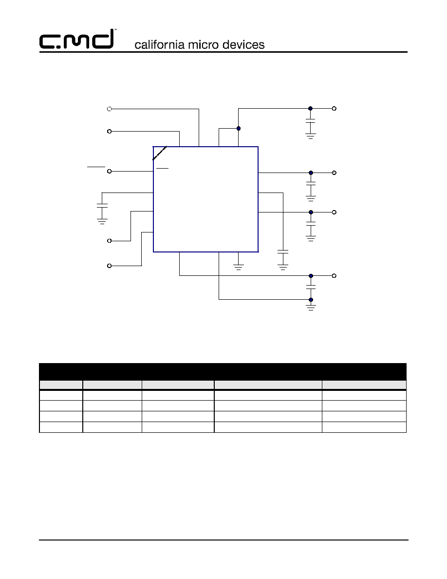
Application Circuit
Power
CT
SHDN
VO
3
SHDN3
CM9107
CC
3
GN
D
3
GN
D
CB1
VO1
VO2
CC2
RS
T
PG
O
O
D
VI
N
3
VI
N
RST
13
+ 3.3V
Good
C
IN
10uF
Reset
16
15
14
1
12
V
OUT1
Reset
+1.8V
3.3uF
11
C
o1
2
C
T
0.01uF
3
10
V
OUT2
+2.84V
C
o2
3.3uF
9
4
Shutdown
LDO 1 & 2
C
b
0.033uF
Shutdown
5
6
7
8
LDO 3
V
OUT3
+2.84V
C
o3
3.3uF
Bill of Materials
BILL OF MATERIALS
ITEM
QUANTITY
REFERENCE
PART
MFR
1
1
C
IN
10µF/10V/1210/X7R
any
2
3
C
o1
, C
o2
, C
o3
3.3µF/10V/1206/X7R
any
3
1
C
T
.01µF/10V/X7R
any
4
1
C
B
.033µF/10V/X7R
any
©
2006 California Micro Devices Corp. All rights reserved.
07/11/06
490 N. McCarthy Blvd., Milpitas, CA 95035-5112
l
Tel: 408.263.3214
l
Fax: 408.263.7846
l
www.cmd.com
9

PRELIMINARY
CM9107
Mechanical Details
TQFN-16 Mechanical Specifications
The CM9107-00QE is supplied in a 16-lead, 4.0mm x
4.0mm TQFN package. Dimensions are presented
below.
For complete information on the TQFN16, see the Cal
ifornia Micro Devices TQFN Package Information doc
ument.
PACKAGE DIMENSIONS
Package
TQFN-16 (4x4)
Leads
16
Dim.
Millimeters
Inches
Min
Nom
Max
Min
Nom
Max
A
0.70
0.75
0.8
0.027 0.029 0.031
A1
0.00
0.02
0.05
0.000 0.001 0.002
A3
0.203 REF
.008
b
0.25
0.30
0.35
0.010 0.012 0.014
D
3.85
4.00
4.15
0.152 0.157 0.163
D1
2.40
2.50
2.80
0.094 0.098 0.110
E
3.85
4.00
4.15
0.152 0.157 0.163
E1
2.40
2.50
2.80
0.094 0.098 0.110
e
0.65 BSC.
0.026
L
0.40 BSC
0.016
# per
tape and
reel
3000 pieces
Controlling dimension: millimeters
A3 A1
0.10 C
0.08 C
A
SIDE VIEW
Mechanical Package Diagrams
D
E
0.15 C
0.15 C
BOTTOM VIEW
TOP VIEW
e
b
L
0.10
C A B
M
16X
D1
E1
Pin 1 Marking
Package Dimensions for 16-Lead QFN
©
2006 California Micro Devices Corp. All rights reserved.
10
490 N. McCarthy Blvd., Milpitas, CA 95035-5112
l
Tel: 408.263.3214
l
Fax: 408.263.7846
l
www.cmd.com
07/11/06