PRELIMINARY
CM9112
Dual Inputs Dual Outputs High Accurate Fast Charger
Features
∑
Monolithic linear charger requires no inductors,
external sense resistors or blocking diodes
∑
4.75V to 6.50V operating input voltage range
∑
It can support up to 30V on Adaptor input and 7V
on USB input
∑
Up to 1.5A total system and charging current
∑
Provides power to the host system and charges
the battery at the same time
∑
Supports AC wall adapter and USB input
∑
4.2V/450mA, available for host system under
Adapter input
∑
It provides 0.5% accuracy of CV mode for 4.2V
∑
An optional 0.1µF cap on CT pin programs 30 min./
60 min. timeout for Precharge/Termination.
∑
Two Thermal limits controls chip temperature and
prevents overheating
∑
Remote sensing pin for Battery voltage
∑
Pin to pin shortage protection
∑
Maximum of 1µA battery drain current
∑
Optional Battery thermistor (NTC) interface
∑
TQFN-16, RoHS compliant lead-free package
Applications
∑
Cellular phones and smart phones
∑
Pocket computers and PDAs
∑
Digital Still Camera
Product Description
The CM9112 is an integrated linear-mode charger for a
single-cell, Lithium-ion battery. It provides both charg
ing current for the battery and power for the host sys
tem. It can deliver charging current up to 1A and
system current up to 450mA at the same time. It takes
power either from AC Adapter or USB Adapter. When
both are present it automatically chooses AC Adapter
as input.
It requires no external blocking diodes or current sense
resistors and uses 2 external resistors to program dif
ferent charging current under AC Adapter or USB
inputs.
The CM9112 provides Precharge Mode, Constant Cur
rent Mode (Fast-charge), Constant Voltage Mode and
Termination by low current detection. Programmable
timeout for Precharge and Termination and Thermistor
interface to check Battery Temperature are optional
available to the users.
The CM9112 is protected against the use of a wrong
high voltage Adapter up to 30V. An antiringing protec
tion on Adaptor input allows the use of a cheaper adap
tor without need of a shock inductor.
Pin to pin shortage protection makes it friendly to the
users against accidental handling during mounting or
checking. The CM9112 is packaged into a miniature
16-pin TQFN package and operates between ≠40∞C
and 85∞C ambient.
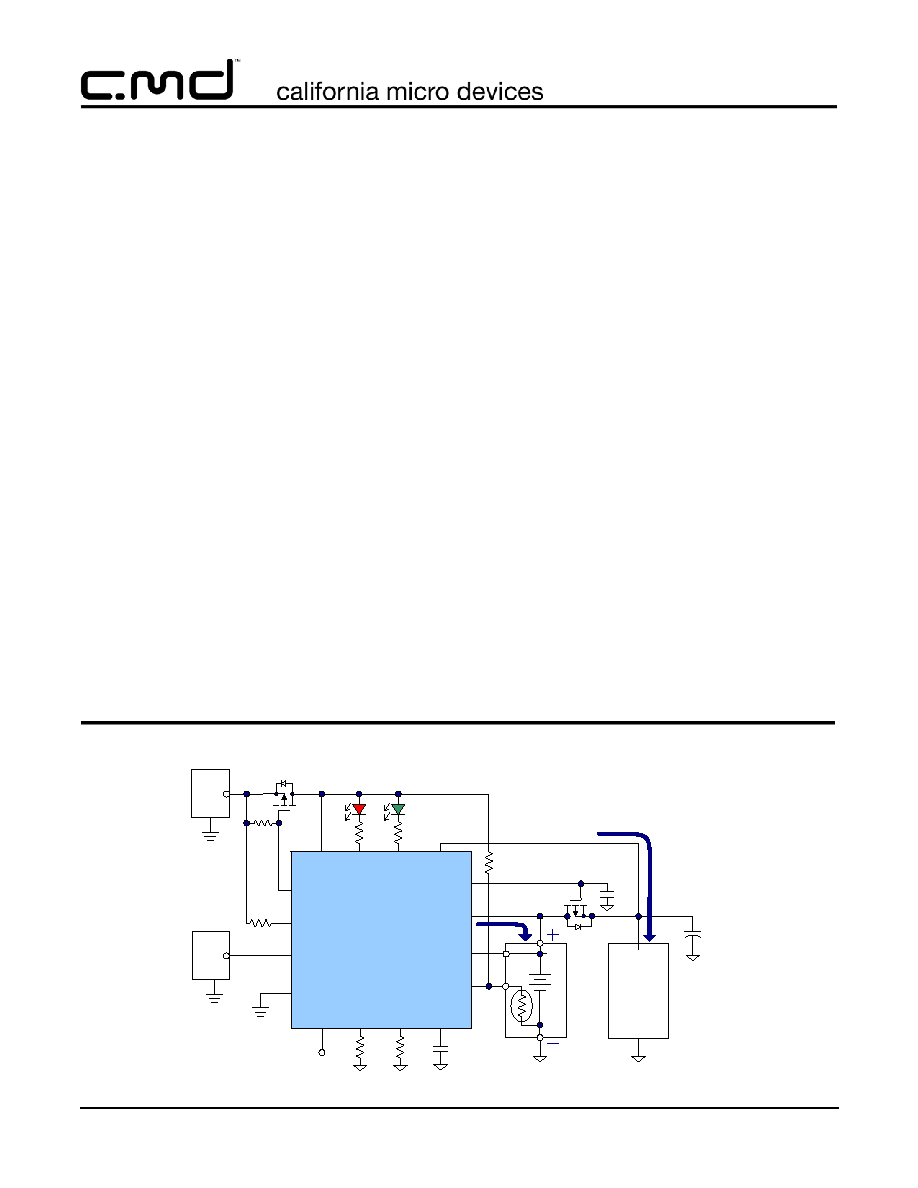
Typical Application
AD
(AC
Adapter )
USB
Q2
Li
-
i
o
n
B
a
t
t
er
y
0.1u
5k
4k
Q1
NTC
VAD
VSYS
GND
VOUT
VREF
THERM
ISET2
USB
ENA
CM9112
ISET1
CT
STAT2
VIN
GAD
BSEN
STAT1
1k
1k
2.5k
0.1u
SYST
EM
4.2V/450mA
10k
33
4.7u
©
2006 California Micro Devices Corp. All rights reserved.
07/06/06
490 N. McCarthy Blvd., Milpitas, CA 95035-5112
l
Tel: 408.263.3214
l
Fax: 408.263.7846
l
www.cmd.com
1
PRELIMINARY
CM9112
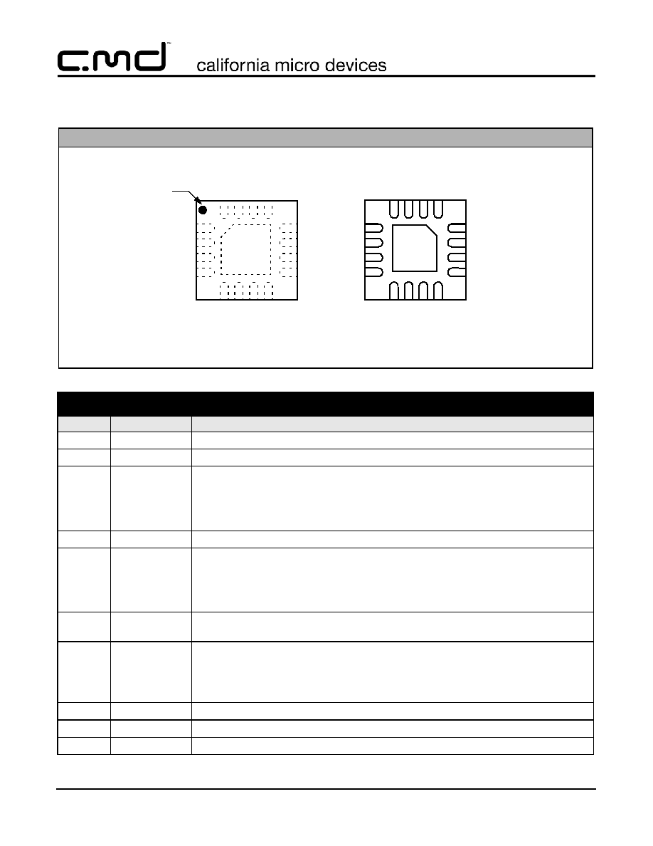
Package Pinout
PACKAGE / PINOUT DIAGRAM
CM9112-00QE
4
3
2
1
9
10
11
12
5
6
7
8
16
15
14
13
GND
PAD
BOTTOM VIEW
(Pins Up View)
TOP VIEW
(Pins Down View)
VREF
ISET1
GND
USB
STAT1
THERM
VOUT
BSEN
VI
N
VA
D
GAD
VS
YS
ISE
T
2
ENA
CT
ST
A
T
2
4
3
2
1
9
10
11
12
5
6
7
8
16
15
14
13
CM91
12
00QE
Pin 1
Marking
16-Lead TQFN Package (4mm x 4mm)
Note: This drawing is not to scale.
PIN DESCRIPTIONS
LEAD(s)
NAME
DESCRIPTION
1
USB
USB compliant power input pin.
2
GND
Ground pin.
3
ISET1
Pin to set the maximum USB input current; Also, reflects actual charging current. A
resistor between this pin and ground sets the charge current,
I
CH
,
R
ISET1
1000
◊ 2.5V
I
CC
= ------------------------------
4
VREF
4.2V, 2mA reference output pin.
5
ISET2
Pin to set the maximum charging current in the Fast charge (CC) mode. Also,
reflects actual charging current. A resistor between this pin and ground sets the
charge current, I
CH
,
R
ISET2
1000
◊ 2.5V
I
CC
= ------------------------------
6
ENA
Enable pin. Logic high (default value) enables charging. Logic low disables charg
ing. ENA does not effect the VSYS output.
7
CT
Pin for capacitor, C
T
, for programming the Precharge and Termination timeout
period.
Timeout1[min]=300 x C
T
[
F]
Timeout2[min]=600 x C
T
[
F]
8
STAT2
Charging status indicator 2 pin (open-drain output).
9
STAT1
Charging status indicator 1 pin (open-drain output).
10
THERM
Thermistor input pin from battery monitoring circuit.
©
2006 California Micro Devices Corp. All rights reserved.
2
490 N. McCarthy Blvd., Milpitas, CA 95035-5112
l
Tel: 408.263.3214
l
Fax: 408.263.7846
l
www.cmd.com
07/06/06

PRELIMINARY
CM9112
Ordering Information
PIN DESCRIPTIONS
11
VOUT
Charger output pin (Battery/RF High Power).
12
BSEN
Battery voltage remote sense pin.
13
VSYS
Power output pin to the host system 4.2V/450mA.
14
GAD
Gate drive to external P-MOSFET for adapter input pin.
15
VAD
Adapter input voltage pin.
16
VIN
Positive input supply voltage pin, which powers the charger.
PART NUMBERING INFORMATION
Pins
Package
Lead Free Finish
Ordering Part Number
1
Part Marking
16
TQFN
CM9112-00QE
CM9112
00QE
Note 1: Parts are shipped in Tape & Reel form unless otherwise specified.
Specifications
ABSOLUTE MAXIMUM RATINGS
PARAMETER
RATING
UNITS
ESD Protection (HBM)
±1
kV
V
IN
to GND
[GND - 0.3] to +6.5
V
Pin Voltages
VAD, GND to GND
V
OUT
, V
SYS,
USB to GND
ENA, I
SET1
, I
SET2
to GND
STAT1, STAT2 to GND
BSEN
,
V
REF,
CT, THERM to GND
[GND - 0.3] to +30
[GND - 0.3] to +7.0
[GND - 0.3] to +6.5
[GND - 0.3] to +6.5
[GND - 0.3] to +6.5
V
V
V
V
V
Storage Temperature Range
-65 to +150
∞C
Operating Temperature Range (Ambient)
-40 to +85
∞C
Lead Temperature (Soldering, 10sec)
300
∞C
ELECTRICAL OPERATING CHARACTERISTICS
(SEE NOTE 1)
SYMBOL
PARAMETER
CONDITIONS
MIN
TYP
MAX
UNITS
V
AD
VAD Operation range
4.75
5.0
6.50
V
V
USB
USB Operation range
4.50
5.25
V
I
Q
Quiescent Current
Charging modes, exclud
ing current to and STAT1,
STAT2 and THERM pins.
2
mA
©
2006 California Micro Devices Corp. All rights reserved.
07/06/06
490 N. McCarthy Blvd., Milpitas, CA 95035-5112
l
Tel: 408.263.3214
l
Fax: 408.263.7846
l
www.cmd.com
3

PRELIMINARY
CM9112
Specifications (cont'd)
ELECTRICAL OPERATING CHARACTERISTICS
(SEE NOTE 1)
SYMBOL
PARAMETER
CONDITIONS
MIN
TYP
MAX
UNITS
I
SHDN
Shutdown Supply Current
ENA = "LOW", excluding
current to STAT1, STAT2
and THERM pins.
50
100
µA
I
REV
Battery Reverse Current
Both AC Adapter and
USB removed
0.5
1
µA
VAD/USB Supply Voltage
UVLO
VAD
UVLO threshold for VAD
4.75
4.8
4.85
V
OVP
VAD
OVP threshold for VAD
6.2
6.4
6.5
V
UVLO
HYS_VAD
UVLO,OVP Hysterezis for
VAD
300
mV
I
IN_AD
Total input current under
Adaptor input
V
IN
=5.0V; Adaptor in
I
IN_AD
=
I
SYS +
I
VOUT
1700
mA
I
IN_USB
Total input current with USB
plugged-in and Adapter out
V
IN
=5.0V; USB in, Adap
tor out
I
IN_USB
=
2500
R
SET
1
(k)
----------------------------------
mA
USB switch Rds(on)
I
IN_USB
= 500mA
150
200
m
Charger Function
I
PR
Precharge Mode Current
V
OUT
< 3.2V; Adaptor in
0.85 x I
PR
I
VOUT =
I
PR
250
R
SET2 k
( )
-
= --------------------------
1.14 x I
PR
mA
V
OUT
< 3.2V; USB in,
Adaptor out
0.85 x I
PR
I
VOUT =
I
PR
250
R
SET1 k
( )
-
= --------------------------
1.14 x I
PR
mA
V
CC
CC Mode Voltage Threshold
3.20
3.30
3.40
V
I
CC
CC Mode Charging Current V
OUT
> 3.5V; Adaptor in
0.92 x I
CC
I
VOUT =
I
CC
2500
R
SET2 k
( )
-
= --------------------------
1.08 x
I
CC
mA
V
OUT
> 3.5V; USB in,
Adaptor out
0.92 x I
CC
I
VOUT =
I
CC
2500
R
SET1 k
( )
-
= --------------------------
1.08 x
I
CC
mA
V
CV
CV Mode Voltage Threshold
4.190
4.200
4.210
V
I
TERM
Charging Termination Cur
rent
V
OUT
> 4.190V; Adapter
in
0.8 x
I
TERM
I
VOUT =
I
TERM
25
R
SET2 k
( )
-
-
= -------------------------
1.2 x
I
TERM
mA
V
OUT
> 4.190V; USB in,
Adapter out
0.8 x
I
TERM
I
VOUT =
I
TERM
25
R
SET
1
(k)
-
= --------------------------
1.2 x
I
TERM
mA
V
RCH
Recharge Mode Threshold
4.090
4.100
4.110
V
©
2006 California Micro Devices Corp. All rights reserved.
4
490 N. McCarthy Blvd., Milpitas, CA 95035-5112
l
Tel: 408.263.3214
l
Fax: 408.263.7846
l
www.cmd.com
07/06/06
PRELIMINARY
CM9112
Specifications (cont'd)
ELECTRICAL OPERATING CHARACTERISTICS
(SEE NOTE 1)
SYMBOL
PARAMETER
CONDITIONS
MIN
TYP
MAX
UNITS
CT
Constant-temperature
Mode, Limit
(Note 2)
95
105
125
C
OTP
Over-temperature Protec
tion, Limit
(Note 3)
130
140
150
C
OCP
Over-Current Charging
(OCP), Limit
1.5
1.7
1.8
A
R
DSON
R
DSON
of Charger MOSFET I
CC
= 500mA
100
120
150
m
T
PR
Precharge Timeout
(Note 4)
Adaptor in; BSEN < 3.2V,
CT=0.1µF, 1%
27
30
33
Min.
T
TER
Termination Timeout
(Note 4)
Adaptor in; BSEN >
4.19V, CT=0.1µF, 1%
54
60
66
Min.
VREF
V
REF
Regulated Voltage V
REF
I
REF
< 1mA
4.190
4.200
4.210
V
VSYS (Available only with Adapter plugged-in) (Note 5)
R
DSON
MOSFET R
ON
0.25
V
SYS
Output Voltage Load Regu
lation
I
OUT
= 10mA to 300mA
4.1
4.2
4.3
V
I
OUT
= 10mA to 450mA
3.9
4.0
4.1
V
I
SYS
Output Current available
3.9V<VSYS<4.3
10
450
mA
I
LIMIT
Over-Current Shut-down
Threshold
(Note 6)
1200
1500
mA
Control Function
I
BSEN
BSEN Pin Leakage Current V
IN
= 0
0.2
1.0
µA
V
STAT1
V
STAT2
STAT1, STAT2 (Open Drain)
Output Low Voltage
I
SINK
= 5mA
I
SINK
= 20mA
0.1
0.5
V
V
V
IH EN
ENA Input High Level
1.5
V
V
IL EN
ENA Input Low Level
0.4
V
Thermistor Function (Note 7, 8)
V
BH
Battery HOT Voltage
Threshold (THERM Pin)
V
IN
= 5.0V
(Note 9)
0.9 x V
BH
V
BH
= 0.5 x V
IN
1.1 x V
BH
V
V
BC
Battery COLD Voltage
Threshold (THERM Pin)
V
IN
= 5.0V
(Note 9)
0.9 x V
BC
V
BC
= 7/8 x V
IN
1.1 x V
BC
V
Hysterezis of V
BH
, V
BC
80
100
120
mV
Note 1: T
A
= 25∞C unless otherwise specified.
Note 2: When chip temperature reaches 105∞C, the IC's internal thermal limit will maintain this temperature by decreasing the pro
grammed charge current.
Note 3: When chip temperature reaches 140∞C, the IC goes into a latched shutdown mode. It stops charging, stops supplying VSYS
with current from Adapter/USB, and switches VSYS (Baseband) to VOUT(Battery). To resume the charging function, a tog
gle of VAD/USB is required.
Note 4: The timeout can be disabled by connecting the CT pin to VIN. When enabled, both Timeout1 and 2 are proportional to the
value of the capacitor connected on the pin CT. However, the ratio Timeout2/Timeout1 is constant and equal to two. The tim
ing periods are digital, internally generated, based on a clock rate programmable by an external capacitor connected in the
CT pin. Timeout feature is available only with AC Adaptor plugged in. Under USB input, both timeout are disabled to allow
longer charging time due to low input current available.
Note 5: When both the Adapter and USB are removed, VSYS is switched over to battery, through an external MOSFET, Q2.
Note 6: When the VSYS maximum current limit is reached, LDO1 regulates this current by decreasing VSYS. However, VSYS can
not go below VOUT (battery) by more than one diode's forward voltage (Vfwd) due to the body diode of the external MOS
©
2006 California Micro Devices Corp. All rights reserved.
07/06/06
490 N. McCarthy Blvd., Milpitas, CA 95035-5112
l
Tel: 408.263.3214
l
Fax: 408.263.7846
l
www.cmd.com
5
CM9112
PRELIMINARY
Specifications (cont'd)
FET, Q2. When this condition occurs, the battery will provide extra current to keep VSYS constant at Vbatt-Vfwd. This lasts
until the power dissipated in LDO1 triggers the OTP. As a result, there will be no input current to supply either charging or
LDO1. Current will still be available from battery to supply VSYS, through the external Q2. To resume charging (after the
chip temperature drop bellow 120∞C), the VAD/USB inputs must be toggled.
Note 7: This feature can be disabled by connecting the THERM pin to GND.
Note 8: This function requires that Battery Thermistor should be connected between the THERM pin and GND. Another resistor
connected between THERM pin and VIN is required, its value should equal the Thermistor Hot Value (at 50∞C). In order to
catch both the 0∞C and 50∞C thresholds (typical range for Li-ion battery) use Thermistors following 7/1 ratio (Thermistor
COLD/Thermistor HOT=7).
Note 9: If the battery HOT/COLD detection identifies a condition outside the thresholds, the IC stops charging the battery and waits
for the temperature to return to the normal value. During this event, VSYS will continue to be supplied with the required cur
rent.
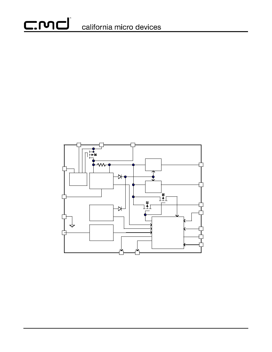
Functional Block Diagram
GAD
USB
VIN
VAD
ISET2
GND
CT
Adapter
Current
Limit
Qc
LDO2
2mA
Charger
Control
OCP
Over-Temp
Limit
OTP
Timer
CM9112
0.03
OVP &
ADOK
Qc / 1000
Current
Mirror
LDO1
450mA
S/D
4.2V
Qb
VSYS
VREF
VOUT
BSEN
ENA
ISET1
THERM
STAT2 STAT1
©
2006 California Micro Devices Corp. All rights reserved.
6
490 N. McCarthy Blvd., Milpitas, CA 95035-5112
l
Tel: 408.263.3214
l
Fax: 408.263.7846
l
www.cmd.com
07/06/06

PRELIMINARY
CM9112
Flow Chart
ISET1
VOUT
R
500
2
I
4.75V<VAD<6.5V
Set Precharge Mode
STAT1
=STAT2=ON
Start Timeout 1
Tj > 150
o
C
Iin > 1.5A
Shut down LDO, VREF,
Stop charging and Latch ;
Set STAT1=STAT2=OFF
Connect VSYS with Battery
through external Q 2
ENA
= High
Yes
BSEN
> 3.3V
Yes
Charge time >
Timeout 1
Stop Charging
Set
STAT1
=STAT2=OFF
Yes
Precharge
Mode
No
No
Set CC mode
STAT1
=ON,
STAT2
=OFF
CC Mode
BSEN
>= 4.200V
No
Set CV Mode
Reset
Timeout 2
CV Mode
No
Yes
BSEN
< 4.200V-100mV
OTP
OCP
Yes
Standby
Mode
No
Timer
Fault
Battery hot ,
cold
or removed
Charge time >
Timeout 2
Stop charging
and Latch. Set
STAT1
=STAT2=OFF
Charge Done or
Battery is not
present
VIN
< BSEN
Shut down LDO1 ,
VREF,
Stop Charging
Connect VSYS with
Battery through
external Q2
Yes
Sleep mode
Shutdown mode
USB
> 4.5V
No
No
Yes
Yes
Yes
Yes
No
No
Battery
Temperature
Checking
No
Precharge in progress
Fast charge in progress
Charge done
STAT2
STAT1
ON
ON
OFF
ON
OFF
ON
Timer fault
Sleep mode
OFF
OFF
OFF
OFF
CHARGE STATE
AD
OK=0
AD
OK=1
AD
OK=1
Yes
AD
OK=1
Start Timeout 1;
VSYS
=4.2V/500 mA
ISET2
VOUT
R
500
2
I
AD
OK=1
ISET2
VOUT
R
500
2
I
Start Timeout 2
Yes
ISET1
VOUT <=
R
120
I
No
No
Yes
ISET2
VOUT<=
R
120
I
ISET1
VOUT
R
500
2
I
No
Yes
AD
OK=1
Yes
Stop charging
Stop Timeout 2;
Set STAT1=OFF
STAT2
=ON
No
Stop charging
Set STAT1=OFF,
STAT2
=OFF
ENA
has no effects
of VSYS output
2.5V<THERM
<4.375V
Note: If Therm is used, during any charging mode, removing a battery will cause the CV mode, then termination, the equivalent
to charge done. Until the battery is returned, the charger will cycle between standby mode and re-charge cycle.
©
2006 California Micro Devices Corp. All rights reserved.
07/06/06
490 N. McCarthy Blvd., Milpitas, CA 95035-5112
l
Tel: 408.263.3214
l
Fax: 408.263.7846
l
www.cmd.com
7

PRELIMINARY
CM9112
Application Information
The CM9112 is an integrated charger with a charging
profile tailored for single-cell graphite electrode (anode)
Li-ion batteries. This linear charger can be powered
from either an AC voltage-source adapter or a USB
port. When both are applied it will automatically select
the AC Adaptor source.
The charger features the three modes required for a
safe and reliable Li-ion charging profile; Precharge,
Fast-charge, and Termination charge. Extensive safety
features include battery temperature monitoring, volt
age and current monitoring and charging time limits.
Two charging status indicators provide charge state
information.
Two different external resistors Riset1,Riset2 allow two
different charging current to be programmed for either
USB adaptor or AC Adaptor. This method allows an
accurate control of USB input current.
Under AC Adaptor input both VSYS (host system) and
VOUT (battery) are simultaneously supplied with the
current required by each oh them, independently.
When the absolute over current limit protection is
reached (1.5A), CM9112 goes into shutdown, latched
mode.
Under USB supply, with AC Adaptor out, CM9112 pro
vide power only to VOUT. The total current available for
VOUT is externally programmed by Riset1.
USB/AC adapter dual input
The CM9112 can support inputs from either a USB bus
or a 5V AC wall adapter.
The USB standard specifies a 5.0V +/-5% bus voltage,
capable of 500mA (High Power peripheral configura
tion) of current. Since desktop and mobile PCs are
equipped with USB or USB2 connectors for interfacing
with peripherals and digital consumer electronics, it is
advantageous to tap the USB's power to charge porta
ble devices such as cell phones.
When using USB input power, the CM9112 will auto
matically select external resistor Riset1 to fix the total
input current. This goes only into VOUT pin and is
intended to charge the battery. However, the system is
connected to the battery through a Schottky diode.
This makes possible some current flowing into VOUT
pin to go not only into Battery but into System too. A
longer charging time will be the result of this. That's
why, under USB input, timeout for charger are disabled.
When using AC Adaptor power, CM9112 will automati
cally select the resistor Riset2 for charging current. In
addition of this it will provide a free current to VSYS
directly from Adaptor input through a power LDO. This
will be limited to 450mA either by power dissipated on
the chip, or absolute current limit.
When using a constant-voltage, 5VDC nominal, AC
adapter, the semi-regulated voltage to the charger,
after accounting for the conduction losses through the
power cord and connector contacts, is a voltage in the
range of 5.0V to 6.0V. When a valid AC adapter voltage
between 4.75V and 6.5V is detected on the VAD pin,
an external MOSFET, Q1 is turn ON and VAD and VIN
are connected together. An internal power MOSFET
used for USB supply, is turned OFF, so there is no
residual voltage on USB pin due to VAD supply. The
same, when USB is used as input. No residual voltage
in VAD pin.
Charging Li-ion Batteries
Once the CM9112 detects the presence of either a
valid AC adapter or USB input voltage, and checks that
the battery voltage at BSEN is less then V
IN
and that
the battery temperature is within the correct range, it is
ready to charge the Li-ion battery. The controller's
internal counter is reset.
If the battery voltage is deeply discharged (less than
3.2V), the CM9112 will start in the Precharge mode,
charging at 10% of the programmed Fast-charge cur
rent level. See
Figure 1
. While the battery is charging,
the status pins will be set to STAT1=0 and STAT2=0.
The Precharge current will gradually bring the battery
voltage to above 3.2V. If the battery does not reach the
3.2V level, indicative of a defective Li-ion cell, the
CM9112 will turn off the charging process after a Pre-
charge timeout period (Timeout1, 30 minutes per
0.1µF of CT capacitance). In this case, the status pins
will be set to STAT1=V
IN
and STAT2=V
IN
.
©
2006 California Micro Devices Corp. All rights reserved.
8
490 N. McCarthy Blvd., Milpitas, CA 95035-5112
l
Tel: 408.263.3214
l
Fax: 408.263.7846
l
www.cmd.com
07/06/06
PRELIMINARY
CM9112
Application Information (cont'd)
Cu
r
r
e
n
t
Pre-
Constant
Termination CV
Condition
Current
Char
Cur
ging
rent
Ch
Vo
argin
ltage
g
4.0V
3.0V
2.0V
Figure 1. Typical Li-ion Battery Charging Process
Once the battery voltage exceeds the 3.3V threshold,
the CM9112 enters the Fast-charge, constant-current
(CC) mode. The status pins will be set to STAT1=0 and
STAT2=V
IN
. During the CC mode, the charging current
is limited by the maximum charging current, pro
grammed with a single resistor between ISET1 for USB
and ISET2 for adaptor:
2.5V
◊ 1000
I
FASTCHG(
max
)
= -------------------------------
R
ISET1 2
,
Most battery manufactures recommend an optimal
charging current for their battery. This is typically a time
ratio related to the battery capacity, with a value of .7C
to 1C, once the battery is above the Precharge voltage
level. For example, a 750mAh capacity battery with
recommended charge of .7C could have I
CC
set for
about 525mA, with R
ISET2
equal to 4.75k
, 1%.
The actual Fast-charge current might be further limited
by the maximum chip temperature limit, determined by
the power dissipation on the CM9112 chip, the ambient
temperature (T
A
), and the junction-to-ambient thermal
resistance, Rth
(JA)
. The current requested by System,
ISYS, might have a significant contribution to the power
dissipated on the chip and reduction of the charging
current. So, it is recommended to reduce as much as
possible the ISYS current during charging. However,
there is not timeout for fast charge period. So, there is
no risk to stop the charging, just delay of it.
When the battery voltage reaches 4.200V it goes into
CV mode and CM9112 turn from a constant current
source to a constant voltage source. As a result, the
charging current start dropping. The actual charging
current is now determined by the differential voltage
(4.20V ≠ V
OC
) and the internal impedance, R
internal
, of
the Li-ion battery-pack. When it reaches termination
current limit, stop charging is triggered and the Battery
is fully charged.
Following the Termination mode, the charger will enter
the Standby mode. The status pins will be set to
STAT1=V
IN
and STAT2=0.
If the wall adapter or USB input is left plugged-in while
in the Standby mode, the charger will continue to mon
itor the battery voltage. It automatically re-charges the
battery when the battery voltage drops below the re
charge threshold. When the adapter is removed, the
CM9112 will drain less than 1µA from the battery.
V
IN
I
SYS
V
OUT
I
CH
Conventional
Floating
Charger
System
V
BAT
Figure 2. Conventional Charger
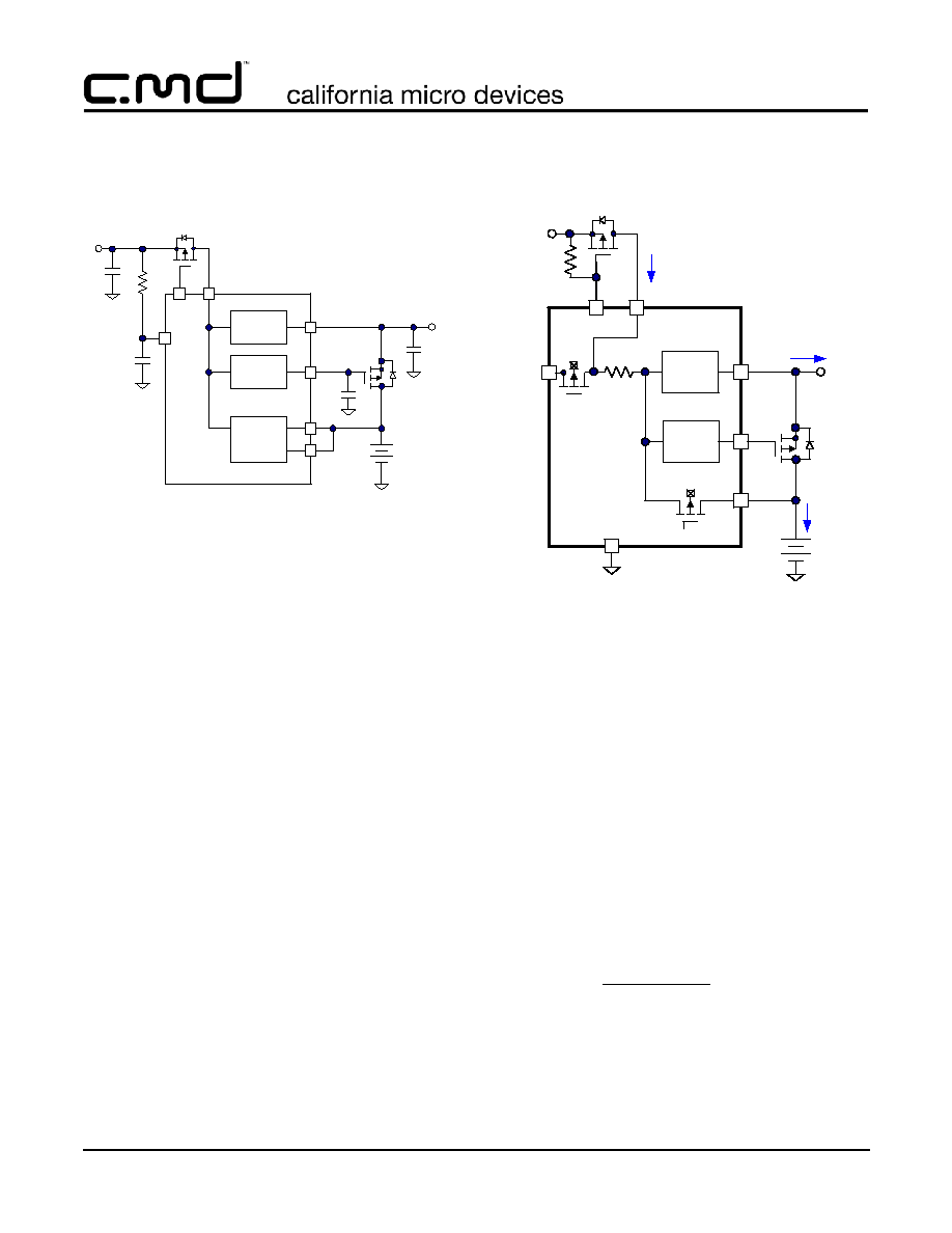
Limitations of Conventional Chargers
In a conventional floating charging architecture, the
system load is always tied directly to the battery, as
shown in
Figure 2
. If the adapter is charging a deeply
discharged battery in the Precharge mode, the system
input voltage will be held below 3.2V, the same voltage
as the battery voltage. This charger output voltage may
be too low to allow a user to use the system, even for
non-transmitting (low power) tasks, such as composing
emails. Further, in the Precharge mode, the battery
charge current is typically limited to 100mA or less. If
the system is trying to power up, it may draw more cur
rent than the Precharge current limit allows. In this con
dition, the system will continue to drain power from the
battery, potentially causing the battery charger to
remain stuck in a Precharge mode indefinitely. After the
Precharge timeout expires, the charger, thinking it has
a defective battery, will shut down, and the battery is
never charged beyond the Precharge mode.
©
2006 California Micro Devices Corp. All rights reserved.
07/06/06
490 N. McCarthy Blvd., Milpitas, CA 95035-5112
l
Tel: 408.263.3214
l
Fax: 408.263.7846
l
www.cmd.com
9
PRELIMINARY
CM9112
Application Information (cont'd)
When using conventional floating charger with the sys
tem load connected directly to the battery, and in the
CC mode, where a higher current limit is available, for
example, the system can draw a continuous load cur
rent of 300mA. However, since the system is always
tied to the battery, the charger IC has no way to differ
entiate the system power demand from the battery
charging demand. The charger will limit the total output
current to 300mA for the system and 1A for charging
the battery. If the battery voltage is low, 3.2V for exam
ple, the charger IC power dissipation will be at its worst
case, or 3.6W. The charger's junction temperature
rises quickly, triggering the over-temperature (OT) cur
rent foldback. If the system continues to draw a large
current, the battery will then be supplying part of that
load current; putting the battery is in a discharge mode,
rather than in a charge mode. The battery voltage will
continue to drop, potentially falling back into a Pre-
charge mode condition, and upsetting the charging
sequence or forcing the charger to shut down.
Even the charger power dissipation due to the system
load alone:
PD1 = 1.0A
◊ (5V ≠ 3.2V)= 1.8W
may already exceed the chip's thermal limit and cause
OTP to trigger.
The CM9112 Dual Outputs Charge Advantage
To overcome these issues, the CM9112's Fast-charge
architecture separates the system power output
(LDO1) from the battery charging power output. See
Figure 3
. With a separate output, the power dissipation
contributed by LDO1 in a condition similar to the one
above is now only:
PD1 = 1.0A
◊ (5V ≠ 4.2V)= 0.8W
In other words, the LDO1 can support the system load,
free from the hindrance of the charger, regardless of
the battery voltage level. The user can continue use
the host system, even when the battery charge voltage
is very low, when there is a defective battery, or there is
no battery present.
V
IN
I
SYS
V
BAT
I
CH
CM9112
System
BSEN
VSYS
VREF
VOUT
LDO1
Charger
4.2V
Figure 3. Dual Outputs Charger
Since the CM9112 provides an independent power
path to the system, as soon as an adapter is plugged-
in, the user can use the system power, even if the bat
tery is dead or in the Precharge mode.
Charging Current Foldback in the Over-
temperature Condition
A limitation of linear chargers is that they are vulnera
ble to over-temperature conditions. The CM9112 will
throttle down the charging current when the chip junc
tion temperature reaches 105∞C (with 10∞C of hys
terezis). This protects the charger IC and its nearby
external components from excessive temperature.
The Charger IC junction temperature is determined by
several factors in the following equation:
T
J
=
T
A
+ PD + Rth
(JA)
(1)
The Rth
(JA)
is usually determined by the IC package
and the thermal resistance between the package and
the PC board. In particular, a SMD IC package relies
on the underlying PC board copper to move the heat
away from the junction. The key to reducing the ther
mal resistance between the IC package and the under
lying PC board is using a large copper (Cu) area for
solder attach and a large ground plane underneath the
charger IC to conduct the heat away.
The power dissipation (PD in equation 1) of a linear
charger is the product of input-output voltage differen
tial and output current.
©
2006 California Micro Devices Corp. All rights reserved.
10
490 N. McCarthy Blvd., Milpitas, CA 95035-5112
l
Tel: 408.263.3214
l
Fax: 408.263.7846
l
www.cmd.com
07/06/06

PRELIMINARY
CM9112
Application Information (cont'd)
PD =
(V
IN
≠ V
OUT
) ◊ I
OUT
In most cases, V
IN
is fixed at about 5.0V (either the AC
adapter or the USB power input). The CM9112 has two
outputs; one for the charger and one for the system
from LDO1. The total power dissipation is:
PD =
(5V ≠ 4.2V) ◊ I
SYS
+
(5V ≠ V
BAT
) ◊ I
FASTCHG
Highest power dissipation occurs when the battery at
its lowest level (3.2V), when it just starts in the Fast-
charge (CC) mode. Assuming V
IN
= 5.0V, V
BAT
= 3.2V,
I
CC
= 1A, the PD = (5V-3.2V) x 1A = 1.8W. Assuming
Rth
(JA)
= 50∞C/W, then
T = 1.8W x 50∞C/W = 90∞C. If
the ambient temperature (T
A
) is 35∞C, then the junction
temperature (T
J
) could reach 125∞C without over-tem
perature current foldback.
With over-temperature (OT) current foldback, the
CM9112 will throttle down the charging current, allow
ing the junction temperature will reach steady-state
equilibrium of 105∞C, which translates into 1.4W of
power dissipation, or 0.78A of charge current. As the
battery voltage rises during charging, the allowable PD
dissipation is increased. When the battery voltage
reaches 3.6V, a full 1.0A of charging current is allowed.
Dual-Level OTP and OCP
In addition to chip temperature regulation at 105∞C, the
CM9112 provides absolute over-temperature shutdown
protection. In the case of a malfunctioning charger con
trol, high ambient temperature or an unexpectedly high
IC thermal resistance, Rth
(JA)
(for example; due to
faulty soldering of the charger IC chip), the power dissi
pation from LDO1 alone could over-heat the device.
The CM9112 provides an absolute OTP shutdown at
junction temperature of 150∞C.
Similarly, each output, LDO1 and VOUT (ISET2), has
its own current limit. ISET1 provides the total adapter
current limit for adaptive charging current control. How
ever, in case of an inoperative ISET2 setting (for exam
ple; R
ISET2
becomes shorted to ground), ISET1 will
function as backup over-current protection. Combining
the dual-level OTP and the dual-level OCP, the
CM9112 in effect provides four layers of protection
against charger or VSYS over-load faults.
The Need for OVP
There are two primary reasons for adding an input
OVP feature to the CM9112 charger. One is to protect
the charger and the host system when an adapter with
the wrong output voltage is plugged-in. The other is to
protect the charger IC and the system against input
surge voltage resulting from the ringing due to the input
capacitor and an inductive adapter power cord.
Almost all computer peripherals and consumer elec
tronics use AC adapters. It is common to use an LCD
monitor, a printer, a laptop computer, an ADSL or cable
modem, a cell phone, an MP3 player, with all their indi
vidual AC adapters clustered around a power strip. The
output voltages of these adapters vary, yet most of
these use a similar cylindrical style connector at the
device interface. Thus, the chance that a user might
plug-in a wrong adapter should not be taken lightly.
The CM9112 provides over-voltage protection (OVP)
against the plug-in of a wrong adapter, up to an output
voltage of 30V. The CM9112 drives a 30V P-type
power MOSFET as a disconnect switch. The propri
etary OVP design of the CM9112 protects itself and the
host system against the intermittent connection of a
wrong adapter.
Another source of over-voltage comes from voltage
ringing that occurs when an adapter is first plugged-in,
as shown in
Figure 4
. A long power cord from the
adapter output can have an inductance of several µH,
and the input capacitor of a cell phone is typically a
10µF to 100µF ceramic, with very low ESR. Unfortu
nately, the low resistance in the power cord and the low
ESR of the input capacitor provide little dampening to
this LC circuit, resulting in strong ringing, with input
voltage overshoot, when the adapter is first plugged-in.
The ringing could apply a peak voltage twice that of the
nominal adapter output voltage at the input capacitor
point.
The CM9112 can withstand several forms of OVP con
ditions; DC, DC with ringing, or intermittent contact of
any frequency.
©
2006 California Micro Devices Corp. All rights reserved.
07/06/06
490 N. McCarthy Blvd., Milpitas, CA 95035-5112
l
Tel: 408.263.3214
l
Fax: 408.263.7846
l
www.cmd.com
11

CM9112
PRELIMINARY
Application Information (cont'd)
Q1 Gate
Drive
Vdc
Figure 4. Q1 Response to Undamped
Ringing at the Input
Charging status
CM9112 provides two charging status indicator pins:
STAT1 and STAT2. These are open-drain outputs,
which can drive LEDs directly, with up to 20mA of cur
rent sinking capability. Alternatively, the system super
visory microprocessor can monitor the battery charging
status by interfacing with these two pins, using a
100k
pull-up resistor for each pin. See
Table 1
.
CHARGE STATUS
STAT1
STAT2
Precharge in progress
Low -
Low -
Fast-charge in progress
Low -
High -
Charge completed
High -
Low -
Charge suspended
(including thermistor fault,
Precharge or Termination
timeout, OTP, OCP and
ENA pulled low)
High -
High -
Table 1: Charge Status for STAT1, STAT2
Thermistor Interface
Li-ion batteries are prone to overheating when exposed
to excess current or voltage. High heat, combined with
the volatile chemical properties of lithium, can cause
fire in some cases. The CM9112 provides a thermal
interface for over-temperature protection, allowing safe
charging of Li-ion cells.
For safety, manufacturers suggest suspending any
charging above 45∞C and below 10∞C until the battery
reaches the normal operating temperature range.
Charging below freezing must be avoided because
plating of lithium metal could occur. Battery capacity
will be reduced if charged between 0∞C and +10∞C due
to the inefficient charging process at low temperatures.
The CM9112 has incorporated a thermistor interface,
responsible for the temperature control of the battery-
pack through a negative temperature coefficient (NTC)
thermistor attached near the battery-pack. The inter
face surveys the voltage on the THERM pin, which an
input to a window comparator with thresholds associ
ated with two battery-pack fault conditions:
Vtherm<1/2 x V
IN
for Battery Hot
Vtherm>7/8 x V
IN
for Battery Cold
To avoid oscillation near the Vtherm thresholds, both
windows have an associated hysteresis of 200mV.
30K
20K
10K
0
0
o
C
20
o
C
40
o
C
60
o
C
+
Thermistor
Resistance
Vtherm
OK
HOT
COLD
1/2*Vin
Rh(4K)
Rc(28K)
7/8*Vin
Figure 5. Vtherm Windows
If the voltage on the THERM pin either exceeds 7/8 x
V
IN
, or goes below 1/2 x V
IN
, the CM9112 stops charg
ing and STAT1, STAT2 signal a fault condition (both go
high). LDO1 remains fully functional and continues to
provide the necessarily current to VSYS (the Base
band load). The charging resumes only when the volt
age on the THERM pin returns to within the window of
1/2 x V
IN
to 7/8 x V
IN
.
Figure 5
illustrates these win
dows.
The thermistor interface consists of a thermistor con
nected between THERM pin and ground, and a resis
tor, Rtherm, connected between the THERM pin and
©
2006 California Micro Devices Corp. All rights reserved.
12
490 N. McCarthy Blvd., Milpitas, CA 95035-5112
l
Tel: 408.263.3214
l
Fax: 408.263.7846
l
www.cmd.com
07/06/06
CM9112
PRELIMINARY
Because the thermistor is typically located on the bat
tery-pack, removal of the battery-pack will remove the
thermistor, and cause value of voltage at the THERM
pin to go above the window and thus stop charging.
This allows the THERM interface to function also as a
battery present detector.
When using the CM9112 with a dummy battery, without
a thermistor attached, this function can be disabled by
connecting the THERM pin to GND. In this case, the
THERM interface will never provide a fault condition to
stop charge.
If there is no need for the thermistor interface, the
THERM pin could be used as a second ENABLE pin
for charging control. If the system has an additional
control condition for stop charge, then the THERM pin
could be used as a second control input. Connecting
the THERM pin to VIN will stop charging, while pulling
to GND will resume charging.
Timeout Intervals
A programmable timer is used to terminate the Pre-
charge and Termination charge modes. There are
three modes in a normal charging procedure; Pre-
charge, Fast-charge (or CC Mode), and Termination (or
CV Mode). Because the first and the third modes take
place at low currents, any failure of the battery (for
example, excessive leakage current) could cause
these modes to continue indefinitely if there was not a
Timeout limit.
CM9112 provides two Timeout intervals: Timeout1,
which limits Precharge time and Timeout2, which limits
the Termination time. These intervals are digitally pro
duced based on an internal clock signal. Timeout1
counts 131072 (2
17
) clock cycles and Timeout2 counts
262144 (2
18
) clock cycles. The ratio of Timeout2/
Timeout1 = 2 is fixed by the design, but the absolute
Timeout values are programmable by an external
capacitor, Ct, connected between the CT pin and GND.
This capacitor is responsible for the clock cycle rate.
Timeout1 time can be calculated as:
17
13.6ms
Ct
Timeout 1
= 2 x
(in minutes)
0.1uF
60
Application Information (cont'd)
VIN, as shown in
Figure 6
. To determine the proper
value for Rtherm, the thermistor used in the battery-
pack should follow the 7:1 ratio on the Resistance vs.
Temperature curve (for example, Vishay Dale's R-T
Curve 2):
R
cold
(at 0∞C)
---------------------------------------- = 7
R
hot
(at 50∞C)
A thermistor with a room temperature value of about
10k
, or higher, will keep the interface current drain
from VIN low. Choose the Rtherm value equal to R
hot
,
with a 0.5% tolerance. A metal film resistor is best for
temperature stability.
For example, a typically used thermistor for this appli
cation is Vishay Dale's NTHS0603N02N1002J. This
thermistor has a R
hot
(50∞C) = 4k
and R
cold
(0∞C) =
28k
. The thermistor interface will work properly if
Rtherm is 4.02k
, 0.5%. At 25∞C the thermistor value
is 10k
. Therefore, a value of voltage at the THERM
pin will be:
10k
Vtherm
=
◊
5V
=
3.57V 25
o
C
14k
4k
o
Vtherm
=
◊
5V
=
2.5V 50 C
8k
28k
Vtherm
=
◊
5V
=
4.375V 0
o
C
32k
BSEN
Thermistor
Interface
Charger
THERM
VIN
VOUT
CM9112
Battery
Pack
NTC
Rtherm (4k)
Vishay
NTHS0603N02N1002 J
Figure 6. NTC Thermistor Interface
©
2006 California Micro Devices Corp. All rights reserved.
07/06/06
490 N. McCarthy Blvd., Milpitas, CA 95035-5112
l
Tel: 408.263.3214
l
Fax: 408.263.7846
l
www.cmd.com
13

PRELIMINARY
CM9112
Application Information (cont'd)
A value of 0.1µF provides a 13.6ms clock cycle period,
producing 30 minutes for Timeout1 (Precharge) and 60
minutes for Timeout2 (Termination),.
When VIN is applied to a fully discharged battery
(V
BAT
<3.0V), the internal counter starts counting clock
cycles for Timeout1. A constant Precharge current
(10% of the programmed Fast-charging current) then
charges the battery. If Timeout1 elapses before the
battery reaches the 3.3V threshold of the Fast-charge
(CC) mode, charging stops and a Charge Suspended
fault is signaled by the status pins
(STAT1=STAT2=V
IN
). This is a latched status and
charging can only resume by toggling V
IN
.
If the battery voltage attains 3.3V before Timeout1
elapses, the internal counter is reset without any action
from the charging algorithm and the battery goes into
the Fast-charge mode.
During the Fast-charge mode, there is no Timeout
counting, and, in theory, this mode can last indefinitely.
During Fast-charge, the battery could be providing cur
rent to a load. With only part of the available charging
current going into the battery, the charging time will
increase and becomes unpredictable. Thus, a Timeout
interval during this mode is not used, allowing greater
application flexibility.
Once the battery reaches the 4.20V threshold, the Ter
mination (CV) mode begins and the charging current
starts to decrease. At the same time, the internal clock
starts counting again. If Timeout2 elapsed before the
Termination current threshold is reached, charging
stops in a latched status (STAT1=STAT2=V
IN
). It can
resume only by toggling VIN. If the Termination thresh
old is reached before Timeout2 has elapsed, the
counter resets and the charger enters into the Standby
mode.
If a stop charge to the battery is triggered by Timeout1/
Timeout2, it should be noted that VSYS would continue
to provide power to the Baseband load.
Disabling the Timeouts
To allow design flexibility for many different applica
tions, the CM9112 allows disabling the Timeout inter
vals as an option. If the application does not require
Timeout Intervals to control Precharge and Termina
tion, connecting the CT pin to VIN will disable the func
tion. The charging algorithm then will be controlled only
by voltage on the BSENS pin (Battery Sense Voltage).
Mode Summary
Precharge mode
is the typical charge starting mode
for pre-conditioning a deeply discharged battery
(<3.3V). A constant current of 10% of the programmed
Fast-charge current is applied to raise the voltage
safely above 3.3V. The maximum charge time is limited
to the programmed Timeout1 period.
Fast-charge mode
is the constant current charging
mode that applies most of the battery charge. A pro
grammed constant current is applied to bring the bat
tery voltage to 4.2V.
Termination mode
is the final charging mode, where a
constant voltage of 4.2V is applied to the battery until
the charge current drops below 5% or the programmed
Fast-charge current. The charging time is limited by the
programmed Timeout2.
Standby mode
is entered after a successful Termina
tion mode and charging is done. Charging stops but
VSYS continue to be supplied by AC Adaptor input. In
this mode, the battery is monitored, and when its volt
age drops below the re-charge threshold (4.100v), a
new charge cycle begins.
Shutdown≠ not latched mode
is triggered by a charg
ing fault. These include THERM pin voltage outside the
window (battery is too hot, too cold, or removed), or
pulling ENA pin low. The charging resumes if the failure
condition is removed. VSYS is still alive and supply
SYSTEM with current.
Shutdown≠ latched mode
If input current, sensed internally, exceeds 1.5A (OCP),
or the IC junction temperature exceeds 150∞C (OTP).
The shutdown happens again but this time it is latched.
Only by toggling VAD/USB and removing the failure
condition the CM9112 could resume the function.
VSYS is no more supplied with current and an external
Q2 MOSFET connect VSYS with the Battery which
become the system power supplier.
Timer-fault mode
is entered when a Timeout ends
without the battery reaching the proper threshold.
Charging stops and remains stopped until VIN is tog
gled. VSYS will continue to receive power through
LDO1.
©
2006 California Micro Devices Corp. All rights reserved.
07/06/06
490 N. McCarthy Blvd., Milpitas, CA 95035-5112
l
Tel: 408.263.3214
l
Fax: 408.263.7846
l
www.cmd.com
14
CM9112
PRELIMINARY
Smartphones are available in the two leading cell
phone topologies, CDMA and GSM. They each have
unique power demands.
The GSM is a TDMA (Time Division Multiple Access)
system where up to eight users share a transmitting
frequency channel. During transmitting, a GSM phone
can draw up to 2.0A of pulse current from the battery
(588 µs pulse width, at a duty cycle of 1/8).
When charging the cell phone battery and using the
cell phone at the same time, the power amplifier still
needs to draw 2A pulse current, which cannot be met
with an adapter having less than 2A of rated output
current capacity. Most adapters are rated at only 1A. In
order to charge the battery and use the phone at the
same time, the high-power section (mainly the RF
power amplifier), has to be supported by the battery at
all times, even when the adapter is plugged-in. See the
typical configuration in
Figure 7
.
With a discharged battery, the charger begins in the
Precharge mode, which will only supply 100mA or less
of charging current. In the case of very low battery volt
age (typically below 3.2V), the cell phone is prohibited
from transmitting and drawing large current from the
battery.
The CM9112, with its integrated 4.2V, 450mA LDO out
put, can support the low-power section of a cell phone,
such as the system microprocessor, LCD display and
LED backlight for the user interface. In addition, the
CM9112 can supply power to the system for non-trans
mitting application such as reading and composing
email messages, or synchronizing data transfers
between a cell phone and a PC.
The CDMA phone demands lower peak current during
transmitting, typically 600mA peak. All the system
power can be supplied by LDO1 when configured as
shown in
Figure 8
.
Application Information (cont'd)
Sleep mode
is entered when the Adapter or USB is
removed (or is the wrong voltage). Charging stops and
VSYS is connected to the battery through Q2. In this
mode, the CM9112 draws less than 1µA of current
from the battery.
Typical Smartphone Applications
A Smartphone is a cellular or mobile phone with
special computer-enabled features not previously
associated with telephones, such as advanced data
functions. Most mobile phone includes some amount of
memory uses such as storing a phone directory, and
most can send and receive text messages, but a
smartphone can perform many more functions,
including PDA, an internet browser, a TV receiver, a
multi-pixel camera, or an MP3 player. Compared to
standard cell phones, smartphones usually have
larger, more colorful displays, contain processors that
are more powerful, and typically run operating system
software. These features are all packed into a smaller
box. This sophistication requires more battery power
than a simple cell phone.
1. In normal battery operation, Q2 is turned
on, the battery supplies power to both the
RF and Baseband loads.
GSM Phone
2. GSM transmitter requires up to 2.0A of
pulse current. In the charging phase, both
the battery and adapter supply current for
the RF load.
BSEN
VAD
GAD
10u
100
0.1u
Q1
LDO1
LDO2
Charger
VSYS
Q2
VREF
VIN
VOUT
CM9112
0.1u
33u
Adapter
Baseband
Load
RF
Load
Figure 7. GSM phone application
©
2006 California Micro Devices Corp. All rights reserved.
07/06/06
490 N. McCarthy Blvd., Milpitas, CA 95035-5112
l
Tel: 408.263.3214
l
Fax: 408.263.7846
l
www.cmd.com
15
PRELIMINARY
CM9112
Adapter
USB
Q2
Qc
LDO2
2mA
GND
VSYS
VREF
VOUT
0.03
5V
GAD
VIN
LDO1
4.2V
Qb
Q1
I
SYS
I
CH
V
BAT
I
IN
< I
SET 1
=
CM9112
Figure 9. Current paths
In normal operation, Q1 is a fully turned-on switch
when an AC adapter is used. The worse-case power
dissipation for the input PMOS, Q1, is:
P
Q1
= I
SET1
2
R
DS
The MOSFET Q1 and PCB heatsink must be rated for
this power. Q1 functions as a clamp to limit input volt
age transients, and should be selected to handle the
worst-case Drain-to-Source voltage, 30V is suggested.
The R
DS
of Q1 should be low enough so that the volt
age drop across it will not cause V
IN
to drop below the
minimum of 4.5V when the adapter is at its lowest out
put. For example, if the adapter is 4.75V minimum at a
load of 1.0A and ISET1 is programmed to 1.0A:
R
DS
(4 .75
1
V
.0 A
4 .5 V ) = 250 m
Q2 is used to supply power to the system from the bat
tery when not charging (adapter removed, end-of
charge, OCP, OTP, etc.). This current passed through
Q2. The worse case power dissipation for Q2 would
Application Information (cont'd)
1. In normal battery operation, Q2 is
turned on, the battery supplies power to
the system load.
Adapter
2. CDMA transmitter requires less than
500mA current. In the charging phase, the
10u
0.1u
BSEN
VAD
CDMA Phone
GAD
100
Q1
LDO1
LDO2
Charger
VSYS
VIN
System
Q2
VREF
VOUT
adapter alone can supply enough power
for the CDMA system load.
CM9112
0.1u
33u
Load
Figure 8. CDMA phone application
Component Selection
The constant voltage AC Adapter must be selected
carefully to minimize power losses and heat dissipation
in the charger. The input supply should be between 5.0
and 6.0V. The lowest allowable input voltage will mini
mize heat dissipation and simplify the thermal design.
An Adapter rated at 5.0V, 5% at the required input cur
rent will provide adequate voltage for the VAD ADOK
window.
The output of LDO1, VSYS, requires a 33µF or larger
capacitor for good stability and minimum voltage droop
during the battery switchover to VSYS at the end of
charge. A low-ESR type capacitor will improve system
response to load transients. The output of VREF
(LDO2), the Q2 gate drive, requires a .1µF ceramic
capacitor for stability.
The CM9112 drives two external P-channel MOSFETs
(PMOS) to control the charging and system currents.
Refer to
Figure 9
. The most important specifications for
the pass PMOS transistors are current rating, R
DS
and
package power dissipation.
©
2006 California Micro Devices Corp. All rights reserved.
07/06/06
490 N. McCarthy Blvd., Milpitas, CA 95035-5112
l
Tel: 408.263.3214
l
Fax: 408.263.7846
l
www.cmd.com
16

PRELIMINARY
CM9112
Application Information (cont'd)
occur when LDO1 is disabled and the battery must
supply full system load.
P
Q2
= I
sys
2
R
DS
The Q2 and PCB heatsink must be rated for this power.
Layout Considerations
Because the internal thermal foldback circuit will limit
the current when the IC reaches 105∞C it is important
to keep a good thermal interface between the IC and
the PC board. It is critical that the exposed metal on
the backside of the CM9112 be soldered to the PCB
ground. The Cu pad should is large and thick enough
to provided good thermal spreading. Thermal vias to
other Cu layers provide improved thermal perfor
mance.
VIN, VSYS and VOUT are high current paths and the
traces should be sized appropriately for the maximum
current to avoid voltage drops. BSEN is the battery
feedback voltage and should be connected with its
trace as close to the battery as possible.
©
2006 California Micro Devices Corp. All rights reserved.
07/06/06
490 N. McCarthy Blvd., Milpitas, CA 95035-5112
l
Tel: 408.263.3214
l
Fax: 408.263.7846
l
www.cmd.com
17

PRELIMINARY
CM9112
Mechanical Details
TQFN-16 Mechanical Specifications
The CM9112-00QE is supplied in a 16-lead, 4.0mm x
4.0mm TQFN package. Dimensions are presented
below.
For complete information on the TQFN16, see the Cal
ifornia Micro Devices TQFN Package Information doc
ument.
PACKAGE DIMENSIONS
Package
TQFN-16 (4x4)
Leads
16
Dim.
Millimeters
Inches
Min
Nom
Max
Min
Nom
Max
A
0.07
0.75
0.80
0.28
0.030 0.031
A1
0.00
0.05
0.00
0.002
A3
0.20 REF
.008
b
0.25
0.30
0.35
0.010 0.012 0.014
D
3.90
4.00
4.10
0.154 0.157 0.161
D1
1.95 REF
0.077
D2
2.00
2.10
2.20
0.079 0.083 0.087
E
3.90
4.00
4.10
0.154 0.157 0.161
E1
1.95 REF
0.077
E2
2.00
2.10
2.20
0.079 0.083 0.087
e
0.65 TYP.
0.026
L
0.45
0.55
0.65
0.018 0.022 0.026
# per
tape and
reel
3000 pieces
Controlling dimension: millimeters
Mechanical Package Diagrams
A3
0.10 C
0.08 C
SIDE VIEW
D
E
BOTTOM VIEW
TOP VIEW
e
b
0.10
16X
D2
E2
DAP SIZE
1.8 X 1.8
E1
D1
Pin 1 Marking
A1
0.15
0.15
C A
M
A
C
C
L
B
Package Dimensions for 16-Lead TQFN
©
2006 California Micro Devices Corp. All rights reserved.
07/06/06
490 N. McCarthy Blvd., Milpitas, CA 95035-5112
l
Tel: 408.263.3214
l
Fax: 408.263.7846
l
www.cmd.com
18