 | –≠–ª–µ–∫—Ç—Ä–æ–Ω–Ω—ã–π –∫–æ–º–ø–æ–Ω–µ–Ω—Ç: CM9142 | –°–∫–∞—á–∞—Ç—å:  PDF PDF  ZIP ZIP |
©
2006 California Micro Devices Corp. All rights reserved.
04/26/06
490 N. McCarthy Blvd., Milpitas, CA 95035-5112
l
Tel: 408.263.3214
l
Fax: 408.263.7846
l
www.cmd.com
1
CM9142
PRELIMINARY
Features
∑
2.9V to 6V input voltage range
∑
Powers two display backlight and/or flash WLEDs
∑
Low external parts count, requires no inductor and
ballast resistors
∑
Low EMI and reflected ripple
∑
Adaptive charge pump ratio (1x or 1.5x) maximizes
efficiency at both high and low input voltage
∑
Precision current regulation for each output with
2% current matching at 20mA
∑
Programmable LED current via ISET1 and ISET2
∑
Independent Analog and PWM brightness control
∑
Independent current setting for each group
∑
Typical 500-kHz fixed switching frequency
∑
Supports up to 300mA, drives six LEDs regulated
to 50mA each
∑
Less than 10
A shutdown current
∑
Over-current and over-temperature protection
∑
Short circuit protection with auto shutdown
∑
Undervoltage lockout
∑
Soft-start limits start-up inrush current
∑
16 lead TQFN package
∑
Optional RoHS compliant lead free package
Applications
∑
Drive white LEDs for STN/TFT Color LCD back-
lighting
∑
Cell phones, PDAs, with multiple displays
∑
Digital Still Cameras
∑
Flash for DSC
Product Description
The CM9142 is an adaptive fractional switched capaci-
tor (charge pump) regulator optimized for driving two
groups, 4 and 2, of white LEDs Each group features
individual ON/OFF controls and individually set current.
Each LED's driver current is matched to within 2% for
uniform intensity. It supports an input voltage range of
2.9V to 6V, with undervoltage lockout. A failure detec-
tion circuit prevents the loss of power when one or
more LEDs fail (short or open). Internal over-tempera-
ture and over-current management provide short circuit
protection.
The CM9142 regulates up to 300mA of output current
to drive WLEDs, allowing up to 50mA per LED channel.
The maximum LED current for each group is pro-
grammed with external resistors. Master plus two inde-
pendent enable inputs allows for Analog and PWM
brightness control for each display. Either display can
also be used for a camera flash. In full shutdown mode,
the CM9142 draws only 10
A.
The CM9142 automatically selects the most efficient
charge pump ratio based on the operating voltage
requirement of the white LEDs. The proprietary design
architecture maintains high efficiency (> 80%), and at
low V
IN
provides longer battery life. With a high V
IN,
or
when the adapter is powered, it provides cool reliable
operation.
The CM9142 is available in a compact 16 lead TQFN
package. It can operate over the industrial temperature
range of -40∞C to 85∞C.
R
SET2
R
SET1
CM9142
CM9142
VIN
1.0uF
2.9V to 6.0V
1.0uF
1uF
C1P C1N
C2P C2N
GND
EN
EN
ISET1
ISET2
VOUT
LED1
LED2
LED3
LED5
LED6
1uF
Display 1
Display 2
LED4
on
off
Enable
PhotonIC
TM
Typical Application
Two Group, 4 and 2, WLED Driver, Different Current Settings
©
2006 California Micro Devices Corp. All rights reserved.
2
490 N. McCarthy Blvd., Milpitas, CA 95035-5112
l
Tel: 408.263.3214
l
Fax: 408.263.7846
l
www.cmd.com
04/26/06
CM9142
PRELIMINARY
Ordering Information
Note 1: Parts are shipped in Tape & Reel form unless otherwise specified.
Specifications
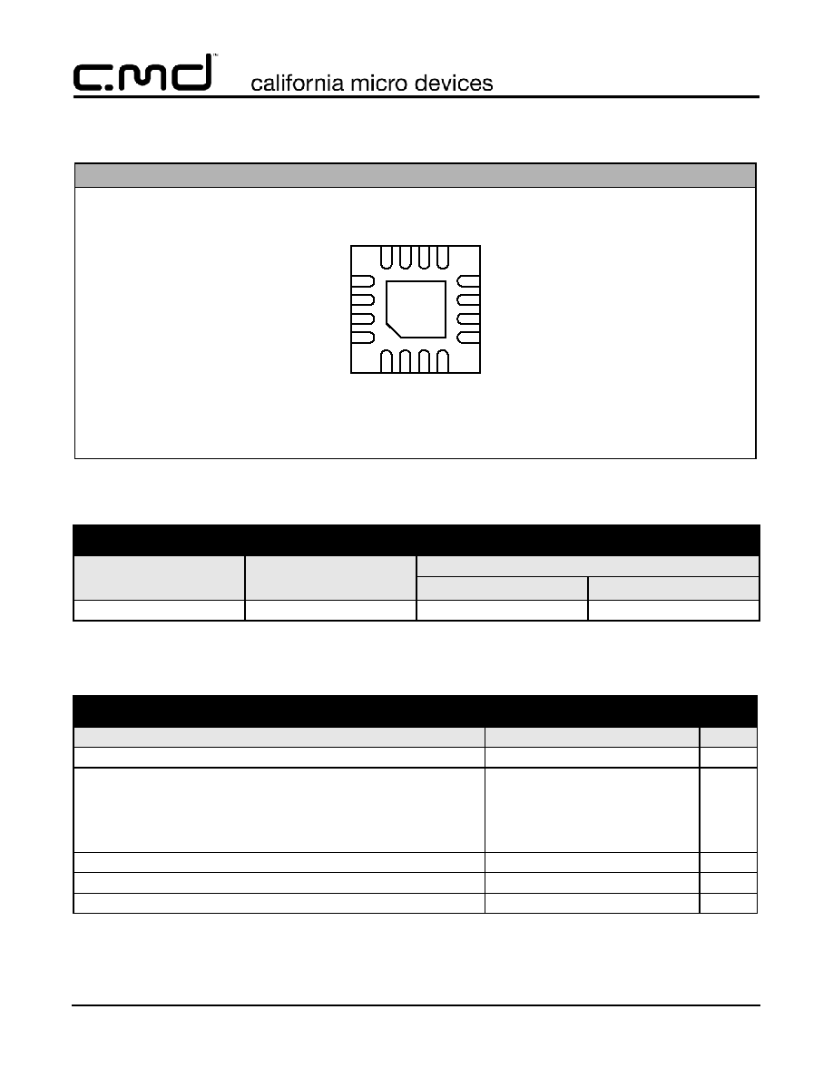
PACKAGE / PINOUT DIAGRAM
Note: This drawing is not to scale.
Bottom View
16-Lead TQFN Package
(4mm x 4mm)
ISET1
VIN
C1P
LED1
EN
GND
C1N
LED4
LE
D2
VO
U
T
LE
D3
C2P
SE
T2
LE
D5
LE
D6
C2
N
4
3
2
1
9
10
11
12
5
6
7
8
16
15
14
13
TQFN16
4 X 4
PART NUMBERING INFORMATION
Leads
Package
Lead-free Finish
Ordering Part Number
1
Part Marking
16
TQFN
CM9142-01QE
ABSOLUTE MAXIMUM RATINGS
PARAMETER
RATING
UNITS
ESD Protection (HBM)
± 2
kV
Pin Voltages
V
IN
to GND
V
OUT
to GND
ISET1, ISET2, EN to GND
All other pins to GND
[GND - 0.3] to +6.0
[GND - 0.3] to +7.0
[GND - 0.3] to +5.0
[GND - 0.3] to +5.0
V
V
V
Storage Temperature Range
-65 to +150
∞C
Operating Temperature Range
-40 to +85
∞C
Lead Temperature (Soldering, 10s)
300
∞C
Package Pinout
©
2006 California Micro Devices Corp. All rights reserved.
04/26/06
490 N. McCarthy Blvd., Milpitas, CA 95035-5112
l
Tel: 408.263.3214
l
Fax: 408.263.7846
l
www.cmd.com
3
CM9142
PRELIMINARY
ELECTRICAL OPERATING CHARACTERISTICS
V
IN
= 3.6V; All outputs are on. Typical values are at T
A
= 25∞C.
SYMBOL
PARAMETER
CONDITIONS
MIN
TYP
MAX
UNIT
S
V
IN
Supply Voltage Range
2.9
6.0
V
V
UVLO
Undervoltage Lockout
All outputs are no load.
1.7
1.8
1.9
V
I
Q
Quiescent Current
1x mode
500
A
I
SD
Shutdown Supply Current
V
EN
< 0.4V
2
10
A
VOUT Charge Pump
V
OUT
Output Voltage
I
OUT
= 0mA to 120mA,
V
IN
= 3.0 to 5.5V
4.2
5.5
V
I
LED TOT
Total I
LED
Current
I
LED1
thru I
LED4
+photoflash
300
mA
ILED
Accuracy of ISET
V
IN
= 3.0V to 5.5V
1
%
Matching current between LED1
to LED6
V
IN
= 4.0V, I
LED 1
to I
LED6
= 20mA
2
5
%
I
LED
per driver
Device total I
LED
< 300mA
50
mA
EN, ISET
V
IH
High Level Input Voltage
1.8
V
IL
Low Level Input Voltage
0.4
Protection
Over-current Limit
400
mA
Over-temperature Limit
135
∞C
Over-temperature Hysteresis
15
∞C
Specifications (cont'd)

©
2006 California Micro Devices Corp. All rights reserved.
4
490 N. McCarthy Blvd., Milpitas, CA 95035-5112
l
Tel: 408.263.3214
l
Fax: 408.263.7846
l
www.cmd.com
04/26/06
CM9142
PRELIMINARY
100 mV/
div
Iin
Vout
Vin
20mA/
div
50mV/
div
1us/div
Typical Waveforms
Cin=C2=C3=Cout=1uF, Iout=120mA
1.5x mode
100 mV/
div
20mA/
div
50mV/
div
Iin
Vout
Vin
1us/div
1.0x mode
Typical Waveforms
Cin=C2=C3=Cout=1uF, Iout=120mA
LED Current vs. Vin
5
10
15
20
25
3.0
3.5
4.0
4.5
5.0
5.5
6.0
Input Voltage (V)
LE
D
C
ur
r
e
n
t
(
m
A
)
Vout
EN
.5ms/div
Startup
Cin=C2=C3=Cout=1uF, Iout=120mA
1V/
div
200mA/
div
2V/
div
Iout=120mA
Iout=60mA
Iout=30mA
Source Current
25
50
75
100
125
150
175
200
3.0
3.5
4.0
4.5
5.0
5.5
6.0
Input Voltage (V)
In
pu
t
C
u
r
r
e
nt
(
m
A
)
Vled=3.2V
Charge Pump Efficiency
60
70
80
90
100
3.0
3.5
4.0
4.5
5.0
5.5
6.0
Input Voltage (V)
E
f
f
i
ci
en
cy
(
%
)
Vled=3.2V
Iout=30mA
Iout=60mA
Iout=120mA
Iin
Typical Performance Curves

©
2006 California Micro Devices Corp. All rights reserved.
04/26/06
490 N. McCarthy Blvd., Milpitas, CA 95035-5112
l
Tel: 408.263.3214
l
Fax: 408.263.7846
l
www.cmd.com
5
CM9142
PRELIMINARY
Pin Descriptions
VIN
C1P
UVLO
OSC
500 kHz
Charge Pump x1, x1.5
C1N
C2P C2N
Current
Sinks
Bandgap
CM9142
Mode Select
Failed LED
Condition
EN
ISET1
GND
ISET2
VOUT
LED1
LED2
LED3
LED5
LED6
LED4
PIN DESCRIPTIONS
LEAD(s)
NAME
DESCRIPTION
1
LED1
Cathode of LED1 pin.
2
C1P
This pin is the plus side of charge pump bucket capacitor C1. Connect a 1.0
F
ceramic capacitor with a voltage rating of 10V or greater between C1N and C1P.
3
VIN
Positive supply voltage input pin. This voltage should be between 2.9V and 6V.
This pin requires a 1.0
F or larger ceramic capacitor to ground.
4
ISET1
Current set and shutdown pin for drivers, active low.Pull high to shutdown the
group.
To set the LED current, a resistor, R
SET
, is connected between this pin and ground.
The regulated LED current is 1000x the current flowing in R
SET
, and is
approximately:
If this resistor is tied to directly ground (and enable function not used) Logic Low =
0, otherwise subtract the voltage drop of the device that drives this pin low.
I
LED
0.66V
LogicLow
(
)
≠
R
SET
----------------------------------------------------- 1000
◊
=
Functional Block Diagram

©
2006 California Micro Devices Corp. All rights reserved.
6
490 N. McCarthy Blvd., Milpitas, CA 95035-5112
l
Tel: 408.263.3214
l
Fax: 408.263.7846
l
www.cmd.com
04/26/06
CM9142
PRELIMINARY
Application Information
The CM9142 is a switched capacitor, charge pump
voltage converter ideally suited for driving white LEDs
to backlight LCD color displays in portable devices.
The CM9142 charge pump is the perfect driver for por-
table applications such as cellular phones, digital still
cameras, PDAs and any application where small
space, compact overall size, low system cost and mini-
mal EMI are critical.
The CM9142 requires only two external switched
(bucket) capacitors, plus an input and an output capac-
itor, providing for a compact, low profile design. In
many applications, these can all be conveniently the
same value of 1.0µF, available in a compact 0805 sur-
face mount package.
The adaptive conversion ratio selects the most efficient
operating mode. When V
IN
is higher than the needed
V
OUT
(V
LED
+V
CURRENT_SINK
), the 1x mode is set.
When the input voltage is below the LED forward volt-
age and a voltage boost is needed, the 1.5x mode is
automatically selected. The 1.5x mode uses a frac-
5
ISET2
Current set and shutdown pin for drivers, active low.Pull high to shutdown the
group.
To set the LED current, a resistor, R
SET
, is connected between this pin and ground.
The regulated LED current is 1000x the current flowing in R
SET
, and is
approximately:
If this resistor is tied to directly ground (and enable function not used) Logic Low =
0, otherwise subtract the voltage drop of the device that drives this pin low.
6
NC
Cathode of LED5 pin.
7
NC
Cathode of LED6 pin.
8
C2N
This pin is the minus side of charge pump bucket capacitor C2. Connect a 1.0
F
ceramic capacitor between C2N and C2P.
9
EN
PWM/Analog input pin. Can be used as second Enable pin, active high. Should tied
high when not used.
10
GND
Ground terminal pin.
11
C1N
This pin is the minus side of charge pump bucket capacitor C1. Connect a 1.0
F
ceramic capacitor between C1N and C1P.
12
LED4
Cathode of LED4 pin.
13
C2P
This pin is the plus side of charge pump bucket capacitor C2. Connect a 1.0
F
ceramic capacitor between C2N and C2P.
14
LED3
Cathode of LED3 pin.
15
VOUT
Charge pump output voltage pin, which connects to the anodes of all LEDs. A 1
F
capacitor to ground is recommended.
16
LED2
Cathode of LED2 pin.
PIN DESCRIPTIONS
I
LED
0.66V
LogicLow
(
)
≠
R
SET
----------------------------------------------------- 1000
◊
=
Pin Descriptions (cont'd)

©
2006 California Micro Devices Corp. All rights reserved.
04/26/06
490 N. McCarthy Blvd., Milpitas, CA 95035-5112
l
Tel: 408.263.3214
l
Fax: 408.263.7846
l
www.cmd.com
7
CM9142
PRELIMINARY
tional charge pump to convert the nominal Li-ion bat-
tery voltage (3.6V) by 1.5 times and regulates the LED
current to the low dropout current sources.
The current regulated sources maintain constant LED
drive in the presence of supply voltage fluctuations. All
LEDs are driven with the same current, even when they
have slightly different forward voltages. The individual
current sources sense the current through each LED
and match this current to less than 2% for uniform
brightness across the color LCD display.
The CM9142 drives up to four WLEDS in group one
and two WLEDs in the second group. The maximum
current programmed by R
SET
determines the maxi-
mum intensity of each group's display; the displays can
be further dimmed by PWM control applied to its ISET1
or ISET 2 pin.
CM9142 Operation
When a voltage that exceeds the undervoltage lockout
threshold (UVLO) is applied to the VIN pin, the
CM9142 initiates a softstart cycle, typically lasting
100
S. Softstart limits the inrush current while the
output capacitors are charged. Following softstart, the
CM9142 next determines the best conversion ratio (1x
or 1.5x).
The 1.5x mode employs a fractional charge pump. The
charge pump uses two phases from the internal oscilla-
tor to drive switches that are connected to the bucket
capacitors, C1 and C2, as shown in
Figure 1
. In the
first switch position, the bucket capacitors are con-
nected in series and each are charged from Vin to a
voltage of V
IN
/2. The next phase changes the switch
positions so that C1 and C2 are in parallel, and places
them on top of V
IN
. The resulting voltage across C
OUT
is then; V
IN
+1/2V
IN
= 1.5 x V
IN
.
Figure 1. Switch Operation
The CM9142 has over-temperature and over-current
protection circuitry to limit device stress and failure dur-
ing short circuit conditions. An overcurrent condition
will limit the output current (approximately 400~600mA)
and will cause the output voltage to drop, until automat-
ically resetting after removal of the excessive current.
Over-temperature protection disables the IC when the
junction is about 135∞C, and automatically turns on the
IC when the junction temperature drops by approxi-
mately 15∞C.
Efficiency
A conventional charge pump with a fixed gain of 2x will
usually develop more voltage than is needed to drive
paralleled white LEDs from Li-Ion sources. This exces-
sive gain develops a higher internal voltage, reducing
Charge C1 and C2 to Ω VIN each
VIN
C1
C2
Ω VIN
VOUT
Ω VIN
Transfer Ω VIN charge to top of VIN
VIN
C1
C2
Ω VIN
Ω VIN
C
OUT
VOUT
C
OUT
Application Information (cont'd)

©
2006 California Micro Devices Corp. All rights reserved.
8
490 N. McCarthy Blvd., Milpitas, CA 95035-5112
l
Tel: 408.263.3214
l
Fax: 408.263.7846
l
www.cmd.com
04/26/06
CM9142
PRELIMINARY
the system efficiency and increasing battery drain in
portable devices. A fractional charge pump with a gain
of 1.5x is better suited for driving white LEDs in these
applications.
The CM9142 charge pump automatically switches
between the two conversion gains, 1x and 1.5x, allow-
ing high efficiency levels over a wide operating input
voltage range. The 1x mode allows the voltage to pass
directly through to the output when sufficient input volt-
age is available. As the battery discharges to the point
where any one current source no longer has sufficient
voltage headroom to maintain a constant current regu-
lation, the 1.5x charge pump is enabled.
At nominal loads, the switching losses and quiescent
current are negligible. If these losses are ignored for
simplicity, the efficiency,
, for an ideal 1.5x charge
pump can be expressed as the output power divided by
the input power:
For an ideal 1.5x charge pump, I
IN
1.5 x I
OUT
, and the
efficiency may be expressed as;
Many charge pumps are fixed 2x designs. The ideal 2x
charge pump efficiency can be similarly expressed;
In 1x mode, when the input voltage is above the output
voltage, the ideal efficiency is simply V
OUT
/V
IN
.
The typical conversion efficiency plots for these modes,
with some losses, are shown in
Figure 2
.
Figure 2. Ideal charge pump efficiency
As can be seen, the CM9142, with 1x and 1.5x modes,
has better efficiency in this application than a fixed 2x
charge pump. At low battery voltages, the higher effi-
ciency of the CM9142 charge pump's 1,5x gain
reduces the battery drain. At higher input voltages, typ-
ically seen when the system is running off an AC
adapter, the CM9142, operating the 1x mode, has bet-
ter efficiency than single mode 1.5x or 2x charge
pumps, lowering the power dissipation for cooler circuit
operation and long life.
While the charge pump efficiency is easily determined,
the system efficiency is more difficult due to the current
source outputs, which complicate measuring the output
power. The forward voltage of the white LEDs will vary,
and the constant current sources will adjust to maintain
the current. When comparing systems, it is best to
compare the input current for a specified LED drive
current.
The 1x mode has better efficiency than the 1.5x mode.
Selecting LEDs with low forward voltage (V
LED
)
increases the time spent in the 1x mode as the battery
discharges, extending the operating time.
Failed LED Detection
If a LED is shorted, the CM9142 will continue to oper-
ate and drive the remaining LEDs at the programmed
current. If a LED opens, the other LEDs will still be reg-
ulated at the programmed current.
P
LED
P
IN
-------------
=
IN
SINK
_
CURRENT
LED
IN
OUT
OUT
IN
OUT
OUT
IN
LED
SINK
_
CURRENT
LED
OUT
V
5
.
1
V
9
.
3
,
V
9
.
3
)
V
V
(
For
V
5
.
1
V
I
5
.
1
V
I
)
V
(
P
P
)
V
V
(
V
◊
=
+
◊
=
◊
◊
◊
+
=
P
OUT
P
IN
-------------
3.9V
2.0 V
IN
◊
-----------------------
30
45
60
75
90
3.0
3.5
4.0
4.5
5.0
5.5
6.0
Input Voltage (V)
E
f
f
i
ci
e
n
cy (
%
)
VLED=3.5V
2X
1X-1.5X
dual mode
1.5X
1X
Application Information (cont'd)

©
2006 California Micro Devices Corp. All rights reserved.
04/26/06
490 N. McCarthy Blvd., Milpitas, CA 95035-5112
l
Tel: 408.263.3214
l
Fax: 408.263.7846
l
www.cmd.com
9
CM9142
PRELIMINARY
LED Current Set (ISET)
An external resistor programs a reference current, set-
ting the maximum driver current. This resistor must be
tied to a good analog ground. If it is pulled to ground
through a switch, for example, from the host controller
output, the voltage drop across that switch should not
exceed 10mV.
The voltage at the ISET1 and ISET2 pins is provided
by a .66V bandgap reference. The LED current is
approximately 1000x the current set by the R
SET
resis-
tor, according to the following formula
:
Logic Low is the voltage on device driving this pin to
ground. If the resistor is tied to ground directly, Logic
low = 0. For 20mA LED current, R
SET
33 k. When this
pin is driven high or open, the device will enter a sleep
mode with V
OUT
= 4.5V and, with no load,
I
QUIESCENT
500
A.
Analog Control of Display Intensity
Typically, portable devices control the backlight display
intensity in response to ambient light conditions, or
lower the intensity after a short standby interval to con-
verse battery charge. The luminous intensity of white
LEDs is proportional to the amount of forward current
through them, but the color wavelength emitted is also
dependent upon the forward current. In applications
where color shift is not critical, brightness can be con-
trolled by adjusting the diode's current. A typical white
LED Intensity vs. forward current curve is shown in
Figure 3
.
Figure 3. Typical Luminous Intensity vs.
LED Current
The ISET pins of the CM9142 can be used to connect
an analog DC signal for analog dimming of the white
LEDs, as shown in
Figure 4
This requires an additional
resistor, R, and a DC source voltage, Vc.
Figure 4. Analog LED current adjust
A control voltage, V
C
, applied to the resistor divider will
decrease the current for all LEDs. The maximum LED
current occurs with 0V on V
C
, which is set by R
P
is the
parallel combination of R and R
SET
.
Choose the maximum control voltage, V
C
, which sets
zero LED current, and than determine the resistor ratio.
R
SET
0.66V
LogicLow
(
)
≠
I
LED
----------------------------------------------------- 1000
◊
=
Relative Luminous Intensity
0.0
0.5
1.0
1.5
0.0
5.0
10.0
15.0
20.0
25.0
30.0
Forward Current (mA)
N
o
r
m
a
liz
e
d
t
o
2
0
m
A
CM9142
ISET(1,2)
V
C
R
R
SET
R
P
0.66V
I
LED
max
----------------------- 1000
◊
=
Application Information (cont'd)
©
2006 California Micro Devices Corp. All rights reserved.
04/26/06
490 N. McCarthy Blvd., Milpitas, CA 95035-5112
l
Tel: 408.263.3214
l
Fax: 408.263.7846
l
www.cmd.com
10
CM9142
PRELIMINARY
The resistors can be determined from the equations
below.
For example, a V
C
max of 2.5V and a maximum current
setting of 20mA, R=125k, R
SET
=44.8k.
Figure 5
shows
the control curve.
Figure 5. LED Current Control Curve
The circuit in
Figure 6
is an example of logic dimming
control, which changes the LED forward current in dis-
crete steps. The NMOS source is an open drain (or
open collector if bipolar) device, either the output of a
host controller, or a discrete device. Open drain, or
open collector devices sink current in their active, low
voltage state (logic 0), and are high impedance in their
high voltage, non-active state (logic 1). The open drain
must not be pulled high with an external resistor, but
instead connected only to the current setting resistors.
The parallel combination of R and R
SET
determine the
full intensity current. When the drain goes high, R
SET
determines the lower intensity current.
Figure 6. Logic Signal Dimming
For example, to reduce the luminosity intensity by half,
using the LED curve from
Figure 3
, the current setting
needs to be changed from 20mA to about 8mA. The
values in
Figure 6
will accomplish this, are where
obtained using the following equations;
Additional parallel resistors can be added in the same
way.
PWM Control of Display Intensity
Typically, portable devices control the backlight display
intensity in response to ambient light conditions, or
lower the intensity after a short standby interval to con-
verse battery charge. The CM9142 allows the output to
lower the LED brightness by applying a pulsing (PWM)
signal to EN, as shown in
Figure 7
for group 2. The
waveforms are shown in
Figure 8
.
The white in white LEDs is typically bichromatic, pro-
duced by a blue or UV LED that excites yellow phos-
phors. The two colors combine and the human eye
sees these them as white light. The forward current of
the LED influences the chromaticity, with higher LED
current increasing the blue content of the color.
Using a PWM signal allows the LEDs to be dimmed
without substantially shifting their color balance due to
chromaticity shifts related to changing white LED for-
ward current. The PWM signal causes the LEDs to
Ratio
0.66V
Vc 0.66
≠
V
--------------------------
=
R
R Ratio
◊
(
) Rp
+
Ratio
-------------------------------------------
=
Rset
Ratio R
◊
=
LED Current vs. Vc
0
5
10
15
20
25
0.0
0.5
1.0
1.5
2.0
2.5
Control Voltage, Vc
LED
C
u
r
r
e
nt
(
m
A
)
CM9142
ISET(1,2)
R
R
SET
82.5k
55k
Open Drain
Controller
Output
Rset
1
Rp
1
1
R
(min)
I
1000
*
V
66
.
Rset
(max)
I
1000
*
V
66
.
Rp
LED
LED
-
=
=
=
Application Information (cont'd)

©
2006 California Micro Devices Corp. All rights reserved.
04/26/06
490 N. McCarthy Blvd., Milpitas, CA 95035-5112
l
Tel: 408.263.3214
l
Fax: 408.263.7846
l
www.cmd.com
11
CM9142
PRELIMINARY
operate either at the full ISET current, or at zero cur-
rent. Only the time averaged current changes. Above a
minimum frequency, the human eye will perceive the
change in duty cycle as a change in brightness.
Figure 7. PWM applied to Display 2
The recommended frequency is between 100 Hz and
200 Hz, with a duty cycle greater than 20%. If a fre-
quency of less then 100 Hz is used, flicker might be
seen in the LEDs. The frequency should also be
greater than the refresh rate of the TFT display. Higher
frequencies will cause a loss of brightness control lin-
earity. In addition, higher frequency can cause chroma-
ticity shifts because the fixed rise and fall times of the
PWM signal will shift the forward current.
The PWM signal will cause the average LED current to
be reduced. The average current is determined by the
PWM duty cycle, which can vary from 0% to 100%.
Decreased Duty Cycle will linearly lower LED bright-
ness, 0% Duty Cycle will turn off the display LEDs.
Figure 8. PWM Signal Dimming
Figure 9. Separate PWM signals for each group
CM9142 Design Examples
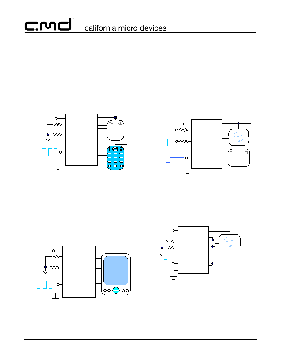
Two Display Cell Phone
Typically, the mobile phone LCD displays (both STN
and mini-TFT) require three to four white LEDs for
backlighting, but as few as two of the newer high-
brightness LEDs can be used. Light guides are used to
distribute the light uniformly behind the LCD. In this
application, four white LEDs are used for the larger
main display (inside the clamshell) and two for the sub-
display.
A typical application for the CM9142 is a dual display
clamshell phone, with an internal main display and an
external sub-display typically used for caller ID and
time of day, backlighting only when there is an incom-
ing call. When the clamshell is opened, the sub-display
backlight goes off and the main display backlight goes
on. See
Figure 10
.
Either display's intensity can be lowered by a PWM sig-
nal applied to R
SET
resistors for the host controller, as
determine by ambient light conditions.
Figure 10. Clamshell Phone Application
CM9142
VOUT
Display
Group2
LED5
LED6
LED1
LED2
LED3
LED4
Display
Group1
VIN
V
BATT
GND
R
SET1
ISET2
EN
ISET1
R
SET2
on
off
Enable
Group2
Group1
PWM
on
off
I
LED (1,2,3)
VOUT
I
SET
EN
PWM signal
CM9142
VIN
LED2
V
BATT
GND
R
SET1
ISET2
EN
ISET1
R
SET2
PWM
on
off
VOUT
Display
Group2
LED5
LED6
LED1
LED3
LED4
Display
Group1
PWM
off
on
on
off
Enable
CM9142
VIN
GND
ISET2
EN
ISET1
VOUT
LED1
LED2
LED3
LED5
LED6
Main
Display
MENU
Sub
Display
Caller ID
LED4
V
BATT
R
SET1
R
SET2
PWM
on
off
Analog
or
Enable
Display 1
on
off
Enable
on
off
Application Information (cont'd)
©
2006 California Micro Devices Corp. All rights reserved.
12
490 N. McCarthy Blvd., Milpitas, CA 95035-5112
l
Tel: 408.263.3214
l
Fax: 408.263.7846
l
www.cmd.com
04/26/06
CM9142
PRELIMINARY
Phone with Keyboard Backlight
The CM9142 can support a wireless phone with LCD
and a backlit keyboard. Group one can drive the back-
light to the LCD, and group two drive the keyboard
backlight. Each group can have a different current set-
ting, and individual PWM signals applied. One or both
groups can have their brightness controlled by a PWM
signal. In the example in
Figure 11
, both are controlled
with one PWM signal.
Figure 11. Phone with Keyboard Backlight
PDA Backlight
The CM9142 can support larger displays such as color
LCDs for PDAs by utilizing both groups. Typically,
larger displays will require four or more WLED back-
lights. With all the drivers set at the same current, uni-
form backlighting can be achieved. EN can be used for
ON/OFF control PWM dimming.
Figure 12
shows a
typical application.
Figure 12. PDA Display Backlight
Camera Flash
The CM9142 can support a camera flash and a display
in digital still cameras as well as in camera equipped
smart phones and PDAs. A typical example would be
the main display is supplied by group 2, and the out-
puts of group 1 are used to support flash white LEDs.
See
Figure 13
. If less current is required for the Main
display drivers in group two, it can be allocated to
group one with the appropriate programming of the
R
SET
resistors.
Figure 13. Display and Flash Application
If a full regulated flash current is needed, both display
outputs can be used to drive flash modules, as shown
in
Figure 14
. In this case, EN controls the flash,
enabling both outputs.
Figure 14. All Flash
Another option, which provides the maximum flash cur-
rent, can be implemented by pulling the cathode of the
flash LED to ground with a switch for the brief duration
of the flash. The example shown in
Figure 15
shows an
example that allows the flash LED to be used as a
CM9142
VIN
V
BATT
ISET1
ISET2
GND
EN
PWM
on
off
R
SET2
R
SET1
LED5
VOUT
LED1
LED2
LED3
LED6
Main
Display
MENU
LED4
CM9142
VIN
ISET1
ISET2
GND
EN
LED5
VOUT
LED6
PDA
Display
LED1
LED2
LED3
LED4
V
BATT
PWM
on
off
R
SET2
R
SET1
CM9142
VIN
V
BATT
GND
R
SET1
ISET2
EN
ISET1
R
SET2
Flash
LED5
VOUT
LED1
LED2
LED3
LED6
LED4
Main
Display
WLED
Flash
Enable
Display 1
on
off
Enable
on
off
R
SET1
R
SET2
Flash
CM9142
VIN
EN
V
BATT
GND
ISET1
ISET2
LED5
VOUT
LED6
LED1
LED3
WLED
Flash
LED4
LED2
Application Information (cont'd)

©
2006 California Micro Devices Corp. All rights reserved.
04/26/06
490 N. McCarthy Blvd., Milpitas, CA 95035-5112
l
Tel: 408.263.3214
l
Fax: 408.263.7846
l
www.cmd.com
13
CM9142
PRELIMINARY
torch light or a preview light in normal operation, and
for full flash when the external switch is turned on. In
this example, the main display intensity is controlled by
two line inputs to ISET1, and the torch light is con-
trolled by S1.
Figure 15. Display, Torch and Full Flash
Capacitor Selection
For proper performance, use surface-mount, low ESR
ceramic capacitors for all four positions. X7R or X5R
ceramic dielectric provides good stability over the oper-
ating temperature and voltage range,
The capacitance and ESR of the external bucket
capacitors will directly affect the output impedance and
efficiency of the converter. A ceramic 1
F capacitor is
recommended.
Reflected input ripple depends on the impedance of
the V
IN
source, such as the PCB traces and the Li-ion
battery, which have elevated impedance at higher fre-
quencies. The input capacitor located near the con-
verter input reduces this source impedance and ripple.
Any ESR from the capacitor will result in steps and
spikes in the ripple waveform, and possibly produce
EMI. Much of the ripple voltage is due to moving cur-
rent charge in and out of the capacitor and the capaci-
tor's impedance at the charge pump frequency. If ripple
voltage or current on the battery bus is an application
issue, add a small input inductor between the battery
and the capacitor, or just increase the capacitor.
For a given output current, increasing the output
capacitance reduces output ripple in the 1.5x mode.
Increasing the output capacitor will also increase star-
tup current and time. In most LED applications, high
frequency output ripple is not a concern because it will
not cause intensity variations that are visible to the
human eye.
Layout Guide
The charge pump is rapidly charging and discharging
the external capacitors, so external traces to the
capacitors should be made wide and short to minimize
inductance and high frequency ringing. The four
capacitors should be located as close as practical to
the charge pump, particularly C1 and C2, which have
the highest dv/dt. Use a solid ground plane, and con-
nect the ground side of C
IN
, C
OUT
and the package
GND as close as practical.
Flash/Torch
CM9142
VIN
V
BATT
GND
VOUT
LED1
LED2
LED3
LED5
LED6
Main
Display
MENU
LED4
Photo Flash
ISET1
ISET2
R
SET2
66K
15K
33K
EN2
EN1
S1
Application Information (cont'd)

©
2006 California Micro Devices Corp. All rights reserved.
04/26/06
490 N. McCarthy Blvd., Milpitas, CA 95035-5112
l
Tel: 408.263.3214
l
Fax: 408.263.7846
l
www.cmd.com
14
CM9142
PRELIMINARY
TQFN-16 Mechanical Specifications
The CM9142 is supplied in a 16-lead, 4.0mm x 4.0mm
TQFN package. Dimensions are presented below.
For complete information on the TQFN16, see the Cal-
ifornia Micro Devices TQFN Package Information doc-
ument.
* This is an approximate number which may vary.
Package Dimensions for 16-Lead TQFN
PACKAGE DIMENSIONS
Package
TQFN-16 (4x4)
Leads
16
Dim.
Millimeters
Inches
Min
Nom
Max
Min
Nom
Max
A
0.80
0.84
0.031
0.033
A1
0.00
0.04
0.00
0.002
A3
0.20 REF
.008
b
0.25
0.33
0.010
0.013
D
4.0 BSC
0.157
D1
1.95 REF
0.077
D2
2.05
2.15
0.081
0.085
E
4.0 BSC
0.157
E1
1.95 REF
0.077
E2
2.05
2.15
0.081
0.085
e
0.65 TYP.
0.026
L
0.55
0.65
0.022
0.026
# per
tube
xx
pieces*
# per
tape and
reel
xxxx pieces
Controlling dimension: millimeters
A3 A1
0.10 C
0.08 C
A
SIDE VIEW
Mechanical Package Diagrams
D
E
0.15 C
0.15 C
BOTTOM VIEW
TOP VIEW
e
b
L
0.10
C A B
M
16X
D2
E2
DAP SIZE
1.8 X 1.8
E1
D1
Pin 1 Marking
Mechanical Details