©
2006 California Micro Devices Corp. All rights reserved.
04/26/06
490 N. McCarthy Blvd., Milpitas, CA 95035-5112
l
Tel: 408.263.3214
l
Fax: 408.263.7846
l
www.cmd.com
1
CM9153
PRELIMINARY
Features
∑
3.0V to 6.5V input voltage range
∑
Two mode operation; 1x and 1.5x
∑
Fixed 4.5V output with initial accuracy of ± 2%
∑
Supports 150mA (@4V) continuous output current
∑
High efficiency at both high and low input voltages
∑
Low external parts count, requires no inductor
∑
PWM brightness control via the ENA pin
∑
650
-
kHz switching frequency
∑
Low shutdown current of <1µA
∑
Soft start prevents excessive inrush current
∑
Over temperature and over current protection
∑
Low output ripple (<1%), low EMI
∑
Input protection provides superior ESD rating,
requiring only standard handling precautions
∑
TDFN-8 or MSOP-8 package
∑
Optional RoHS compliant lead free packageing
Applications
∑
Drive white LEDs to backlight color LCDs
∑
Drive white or RGB LEDs for camera flash
∑
Cellular phones
∑
MP3 players
∑
PDAs, GPS
Product Description
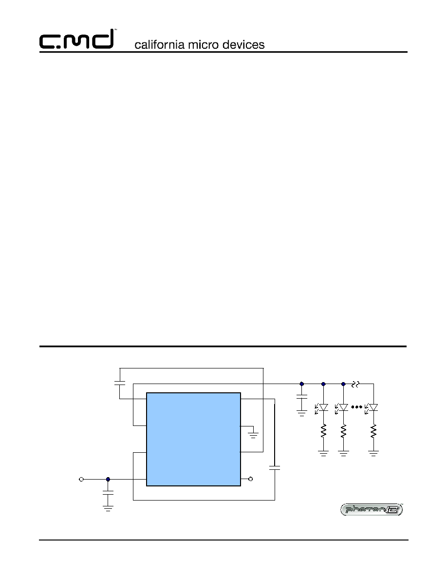
The CM9153 is an efficient 1.5x switched capacitor
(charge pump) regulator ideal for white LED applica-
tions. It has a regulated 4.5V, 120mA output, capable
of driving up to six parallel white LEDs. With a typical
operating input voltage range from 3.0V to 6.0V, the
CM9153 can be operated from a single cell Li-Ion bat-
tery.
It features an efficient, 1.5x charge pump circuit that
uses only two 1.0
F ceramic bucket capacitors and
two small capacitors for VIN and VOUT. The LED
brightness can be adjusted by applying a PWM signal
on the ENA pin.
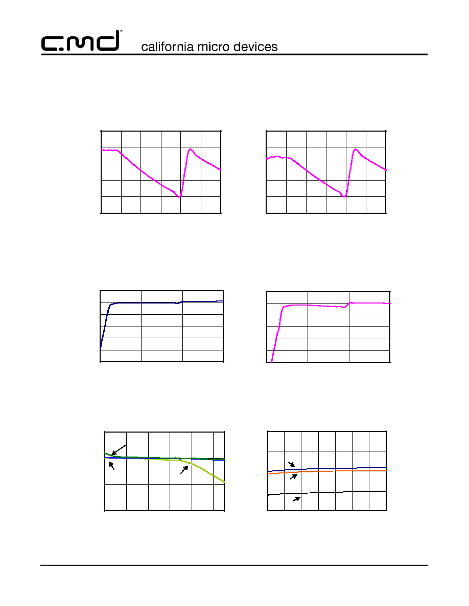
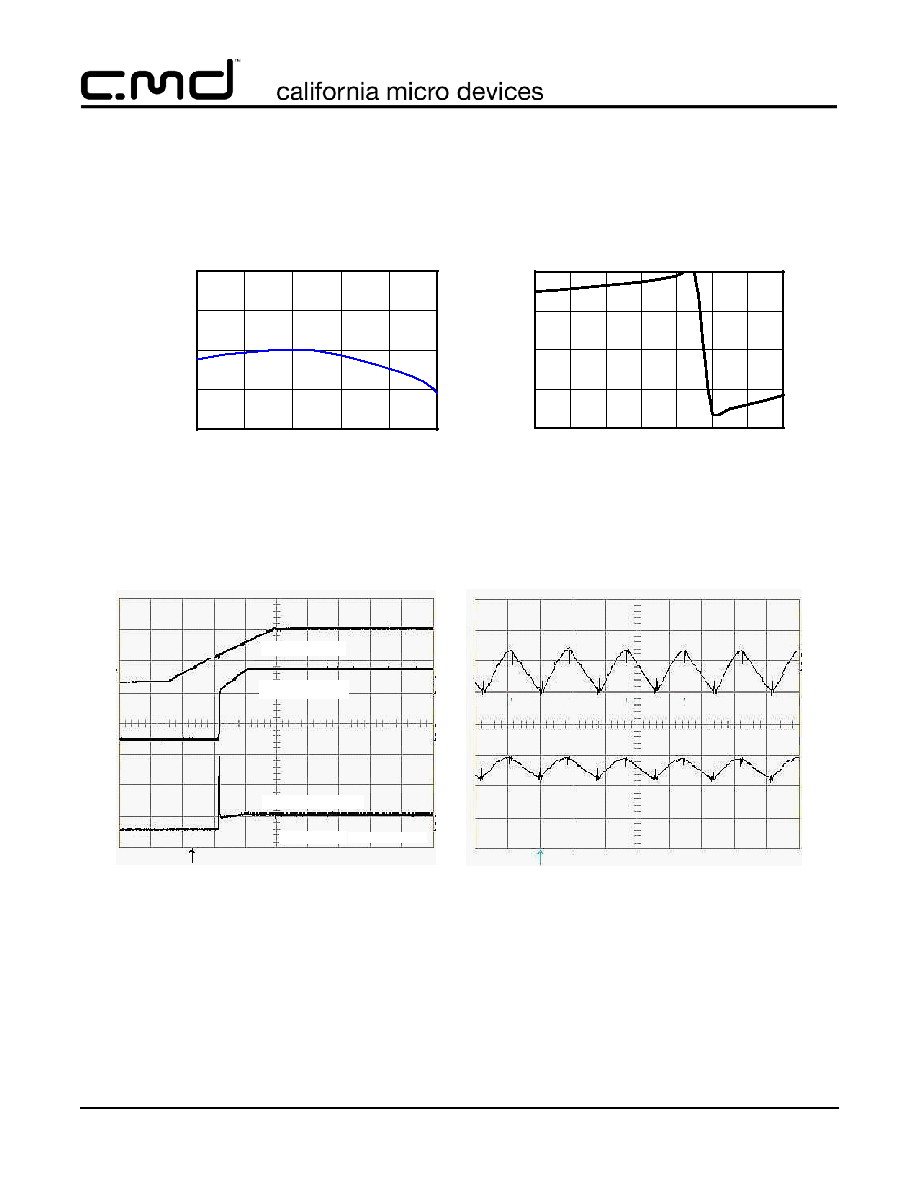
The CM9153 output voltage is regulated to 4.5V, ± 5%
over the line and load ranges. Up 150mA of output cur-
rent is available. A proprietary design architecture
(patent pending) maintains high efficiency (> 80%), at
both below 3.2 V
IN
, resulting in longer battery life, and
above 5.25 V
IN
, when an adapter is plugged in, keep-
ing the part cool. It offers low output voltage ripple, typ-
ically less than 50mV. Internal over-temperature and
over-current management provide short circuit protec-
tion.
The CM9153 is packaged in either a space-saving 8-
lead TDFN or 8-lead MSOP package. It can operate
over the industrial temperature range of ≠25
∞C
to 85
∞C
.
.
1.0uF
1.0uF
4.5V
3.0V to 6.0V
1.0uF
C 1P
V OUT
V IN
C 1N
C 2P
GND
E NA
C 2N
CM9153
1.0uF
PhotonIC
TM
Typical Application
Charge Pump White LED Driver
©
2006 California Micro Devices Corp. All rights reserved.
2
490 N. McCarthy Blvd., Milpitas, CA 95035-5112
l
Tel: 408.263.3214
l
Fax: 408.263.7846
l
www.cmd.com
04/26/06
CM9153
PRELIMINARY
Ordering Information
Note 1: Parts are shipped in Tape & Reel form unless otherwise specified.
Specifications
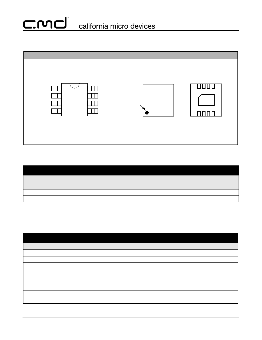
PACKAGE / PINOUT DIAGRAM
Note: This drawing is not to scale.
8 Lead MSOP Package
1
2
3
4
8
7
6
5
C2P
VOUT
C1P
VIN
C1N
GND
C2N
ENA
TOP VIEW
CM9153-01DE
8 Lead TDFN Package
GND
4
3
2
1
4
3
2
1
5
6
7
PAD
5
6
7
8
8
Pin 1
Marking
BOTTOM VIEW
(Pins Up View)
TOP VIEW
(Pins Down View)
CM9153-01MR
PART NUMBERING INFORMATION
Leads
Package
Lead-free Finish
Ordering Part Number
1
Part Marking
8
TDFN
CM9153-01DE
8
MSOP
CM9153-01MR
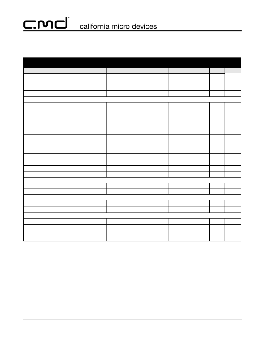
ABSOLUTE MAXIMUM RATINGS
PARAMETER
RATING
UNITS
ESD Protection (HBM)
±
2
kV
VIN to GND
[GND - 0.3] to +6.5
V
Pin Voltages
V
OUT
to GND
C1P, C1N to GND
C2P, C2N to GND
[GND - 0.3] to +6.0
[GND - 0.3] to +4.5
[GND - 0.3] to +4.5
V
V
V
Storage Temperature Range
-65 to +150
∞C
Operating Temperature Range
-40 to +85
∞C
Lead Temperature (Soldering, 10s)
300
∞C
Package Pinout