 | –≠–ª–µ–∫—Ç—Ä–æ–Ω–Ω—ã–π –∫–æ–º–ø–æ–Ω–µ–Ω—Ç: CMC7101AR | –°–∫–∞—á–∞—Ç—å:  PDF PDF  ZIP ZIP |
1
© 2000 California Micro Devices Corp. All rights reserved.
2/00
215 Topaz Street, Milpitas, California 95035 Tel: (408) 263-3214 Fax: (408) 263-7846 www.calmicro.com
CALIFORNIA MICRO DEVICES
CMC7101A
CMC7101A Low Power Operational Amplifier, RRIO, SOT23-5
Features
Tiny SOT23-5 package
Guaranteed specs at 2.7V, 3V and 5V
Low supply current typically 300µA
Rail-to-Rail input and output (RRIO)
Typical total harmonic distortion of 0.01% at 5V
1.0MHz gain-bandwidth
Input common mode range includes V- and V+
Applications
Mobile Communications
Cellular Phones
Portable Equipment
Notebooks and PDAs
C0570499
Product Description
The CMC7101A is a high performance CMOS operational amplifier available in a small SOT23-5 package. Operating with low
supply current, it is ideal for battery operated applications where power, space and weight are critical.
Performance is compatible to the industry standard 7101 SOT Amp, with enhancements of reduced supply current, much
higher output drive current, and enhanced operation at low supply voltage (2.7V). It is the economical solution for 3V to 5V
applications.
Ideal for use in personal electronics such as cellular handsets, pagers, cordless telephones, and other products with limited space
and battery power.
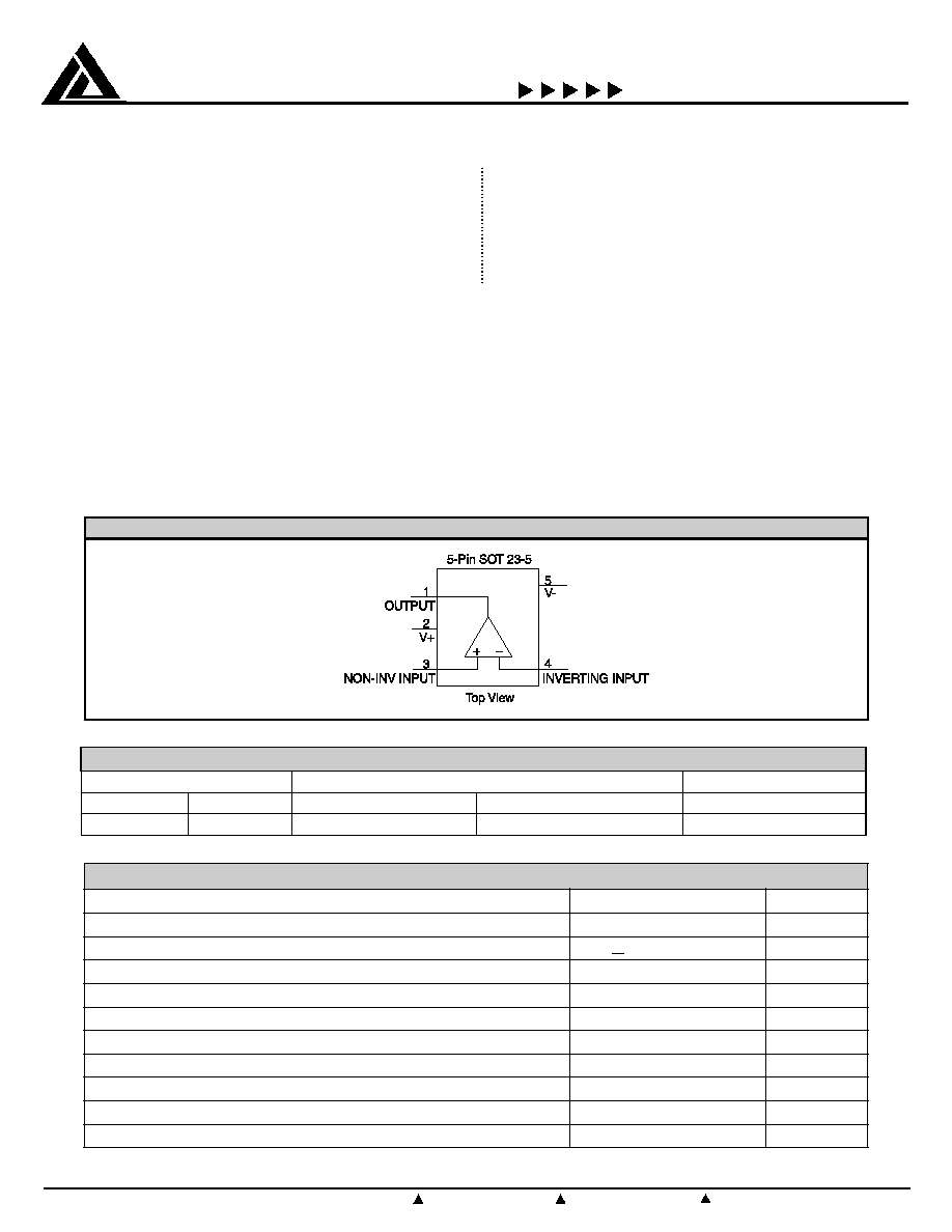
CONNECTION DIAGRAM
N
O
I
T
A
M
R
O
F
N
I
G
N
I
R
E
D
R
O
T
R
A
P
D
R
A
D
N
A
T
S
e
g
a
k
c
a
P
r
e
b
m
u
N
t
r
a
P
g
n
i
r
e
d
r
O
s
n
i
P
e
l
y
t
S
s
e
b
u
T
l
e
e
R
&
e
p
a
T
g
n
i
k
r
a
M
t
r
a
P
5
5
-
3
2
T
O
S
T
/
Y
A
1
0
1
7
C
M
C
R
/
Y
A
1
0
1
7
C
M
C
A
1
0
)
1
e
t
o
N
(
S
G
N
I
T
A
R
M
U
M
I
X
A
M
E
T
U
L
O
S
B
A
r
e
t
e
m
a
r
a
P
g
n
i
t
a
R
t
i
n
U
)
2
e
t
o
n
e
e
s
(
e
c
n
a
r
e
l
o
T
D
S
E
0
0
0
,
2
V
e
g
a
tl
o
V
t
u
p
n
I
l
a
it
n
e
r
e
f
fi
D
+
e
g
a
tl
o
V
y
l
p
p
u
S
V
n
i
P
t
u
p
t
u
O
/
t
u
p
n
I
t
a
e
g
a
tl
o
V
V
3
.
0
-
)-
V
(
,
V
3
.
0
+
)
+
V
(
V
)
-
V
o
t
+
V
(
e
g
a
tl
o
V
y
l
p
p
u
S
5
.
7
V
n
i
P
t
u
p
n
I
t
a
t
n
e
r
r
u
C
5
A
m
)
3
e
t
o
n
e
e
s
(
n
i
P
t
u
p
t
u
O
t
a
t
n
e
r
r
u
C
5
3
A
m
s
n
i
P
y
l
p
p
u
S
r
e
w
o
P
t
a
t
n
e
r
r
u
C
5
3
A
m
).
c
e
s
0
1
,
g
n
ir
e
d
l
o
s
(
.
p
m
e
T
d
a
e
L
0
6
2
o
C
e
g
n
a
R
e
r
u
t
a
r
e
p
m
e
T
e
g
a
r
o
t
S
0
5
1
+
o
t
5
6
-
o
C
)
4
e
t
o
n
e
e
s
(
.
p
m
e
T
n
o
it
c
n
u
J
0
5
1
o
C

©2000 California Micro Devices Corp. All rights reserved.
2/00
215 Topaz Street, Milpitas, California 95035 Tel: (408) 263-3214 Fax: (408) 263-7846 www.calmicro.com
2
CALIFORNIA MICRO DEVICES
CMC7101A
S
N
O
I
T
I
D
N
O
C
G
N
I
T
A
R
E
P
O
)
e
s
i
w
r
e
h
t
o
d
e
i
f
i
c
e
p
s
s
s
e
l
n
u
(
r
e
t
e
m
a
r
a
P
g
n
i
t
a
R
t
i
n
U
e
g
a
tl
o
V
y
l
p
p
u
S
7
.
2 < +
V < 7
V
e
g
n
a
R
.
p
m
e
T
n
o
it
c
n
u
J
0
4
-
< T
J
<
5
8
+
o
C
e
c
n
a
t
si
s
e
R
l
a
m
r
e
h
T
5
2
3
o
W
/
C
S
C
I
T
S
I
R
E
T
C
A
R
A
H
C
G
N
I
T
A
R
E
P
O
L
A
C
I
R
T
C
E
L
E
V
7
.
2
T
r
o
f
d
e
e
t
n
a
r
a
u
g
s
ti
m
il
ll
a
,
d
e
if
i
c
e
p
s
e
s
i
w
r
e
h
t
o
s
s
e
l
n
U
J
R
,
V
0
=
-
V
,
V
7
.
2
=
+
V
,
C
∞
5
2
=
L
M
1
>
l
o
b
m
y
S
r
e
t
e
m
a
r
a
P
s
n
o
i
t
i
d
n
o
C
P
Y
T
T
I
M
I
L
T
I
N
U
V
S
O
e
g
a
tl
o
V
t
e
s
f
f
O
t
u
p
n
I
1
1
.
0
6
V
m
V
C
T
S
O
e
g
a
tl
o
V
t
e
s
f
f
O
t
u
p
n
I
t
fi
r
D
e
g
a
r
e
v
A
1
µ /
V
o
C
I
B
t
n
e
r
r
u
C
s
a
i
B
t
u
p
n
I
1
A
p
I
S
O
t
n
e
rr
u
C
t
e
s
ff
O
t
u
p
n
I
5
.
0
A
p
R
N
I
e
c
n
a
t
s
i
s
e
R
t
u
p
n
I
1
T
R
R
M
C
e
d
o
M
-
n
o
m
m
o
C
o
it
a
R
n
o
it
c
e
j
e
R
V
0 < V
M
C
<
V
7
.
2
0
7
5
5
B
d
V
M
C
e
d
o
M
n
o
m
m
o
C
t
u
p
n
I
V
=
+
V
0
0
V
e
g
n
a
R
e
g
a
tl
o
V
B
d
0
5
>
R
R
M
C
r
o
F
0
.
3
7
.
2
V
R
R
S
P
n
o
it
c
e
j
e
R
y
l
p
p
u
S
r
e
w
o
P
o
it
a
R
V
5
6
.
1
o
t
V
5
3
.
1
=
+
V
V
5
6
.
1
-
o
t
V
5
3
.
1
-
=
-
V
V
M
C
0
=
0
6
0
5
B
d
C
N
I
t
u
p
n
I
e
d
o
M
-
n
o
m
m
o
C
e
c
n
a
ti
c
a
p
a
C
3
f
p
V
O
g
n
i
w
S
t
u
p
t
u
O
R
L
0
0
6
=
0
6
.
2
V
0
1
.
0
V
R
L
K
2
=
0
6
.
2
5
1
.
2
V
0
1
.
0
5
.
0
V
R
L
K
0
1
=
8
6
.
2
4
6
.
2
V
2
0
.
0
6
0
.
0
V
I
S
t
n
e
rr
u
C
y
l
p
p
u
S
0
0
3
.
0
1
8
.
0
µA
R
S
e
t
a
R
w
e
l
S
7
.
0
/
V µs
W
B
G
h
t
d
i
w
d
n
a
B
n
i
a
G
t
c
u
d
o
r
P
6
.
0
z
H
M
3
© 2000 California Micro Devices Corp. All rights reserved.
2/00
215 Topaz Street, Milpitas, California 95035 Tel: (408) 263-3214 Fax: (408) 263-7846 www.calmicro.com
CALIFORNIA MICRO DEVICES
CMC7101A
S
C
I
T
S
I
R
E
T
C
A
R
A
H
C
G
N
I
T
A
R
E
P
O
L
A
C
I
R
T
C
E
L
E
V
3
T
r
o
f
d
e
e
t
n
a
r
a
u
g
s
ti
m
il
ll
a
,
d
e
if
i
c
e
p
s
e
si
w
r
e
h
t
o
s
s
e
l
n
U
J
∞
5
2
=
R
,
V
0
=
-
V
,
V
3
=
+
V
,
C
L
M
1
>
l
o
b
m
y
S
r
e
t
e
m
a
r
a
P
s
n
o
i
t
i
d
n
o
C
P
Y
T
t
i
m
i
L
T
I
N
U
V
S
O
t
e
s
f
f
O
t
u
p
n
I
e
g
a
tl
o
V
1
1
.
0
4
V
m
V
C
T
S
O
t
e
s
f
f
O
t
u
p
n
I
e
g
a
r
e
v
A
e
g
a
tl
o
V
t
fi
r
D
1
µ /
V
o
C
I
B
t
n
e
r
r
u
C
s
a
i
B
t
u
p
n
I
1
A
p
I
S
O
t
n
e
rr
u
C
t
e
s
ff
O
t
u
p
n
I
5
.
0
A
p
R
N
I
e
c
n
a
t
s
i
s
e
R
t
u
p
n
I
1
T
R
R
M
C
e
d
o
M
-
n
o
m
m
o
C
o
it
a
R
n
o
it
c
e
j
e
R
V
<
V
0
M
C
V
3
<
4
7
4
6
B
d
V
M
C
e
d
o
M
n
o
m
m
o
C
t
u
p
n
I
V
=
+
V
0
0
V
e
g
n
a
R
e
g
a
tl
o
V
B
d
0
5
>
R
R
M
C
r
o
F
3
.
3
0
.
3
V
R
R
S
P
y
l
p
p
u
S
r
e
w
o
P
o
it
a
R
n
o
it
c
e
j
e
R
V
8
.
1
o
t
V
5
.
1
=
+
V
V
8
.
1
-
o
t
V
5
.
1
-
=
-
V
V
M
C
0
=
0
8
8
6
B
d
C
N
I
t
u
p
n
I
e
d
o
M
-
n
o
m
m
o
C
e
c
n
a
ti
c
a
p
a
C
3
F
p
V
O
g
n
i
w
S
t
u
p
t
u
O
R
L
0
0
6
=
9
.
2
6
.
2
V
1
.
0
4
.
0
V
R
L
K
2
=
9
.
2
6
.
2
V
1
.
0
4
.
0
V
R
L
K
0
1
=
9
9
.
2
7
.
2
V
1
0
.
0
3
.
0
V
I
S
t
n
e
rr
u
C
y
l
p
p
u
S
3
.
0
1
8
.
0
A
m
R
S
e
t
a
R
w
e
l
S
7
.
0
/
V µS
W
B
G
h
t
d
i
w
d
n
a
B
n
i
a
G
t
c
u
d
o
r
P
6
.
0
z
H
M

©2000 California Micro Devices Corp. All rights reserved.
2/00
215 Topaz Street, Milpitas, California 95035 Tel: (408) 263-3214 Fax: (408) 263-7846 www.calmicro.com
4
CALIFORNIA MICRO DEVICES
CMC7101A
Note 1
Absolute Maximum Ratings indicate limits beyond which damage to the device may occur. Operating conditions indicate ratings for which the
device is intended to be functional, but specific performance is not guaranteed. For guaranteed specifications and the test conditions, see the
Electrical Characteristics.
Note 2
Human body model, 1.5K in series with 100pF.
Note 3
Applies to both single-supply and split-supply operation. Continuous short circuit operation at elevated ambient temperatures can result in
exceeding the maximum allowed junction temperature of 150∞C.
Note 4
The maximum power dissipation is a function of T
J(MAX)
,
JA
and T
A.
The maximum allowable power dissipation at any ambient temperature is PD
= (T
J(MAX)
- T
A
)/
JA
. All numbers apply for packages soldered directly to a PC board.
Note 5
See Application Section
S
C
I
T
S
I
R
E
T
C
A
R
A
H
C
G
N
I
T
A
R
E
P
O
L
A
C
I
R
T
C
E
L
E
V
5
T
r
o
f
d
e
e
t
n
a
r
a
u
g
s
ti
m
il
ll
a
,
d
e
if
i
c
e
p
s
e
si
w
r
e
h
t
o
s
s
e
l
n
U
J
∞
5
2
=
R
,
V
0
=
-
V
,
V
5
=
+
V
,
C
L
M
1
>
l
o
b
m
y
S
r
e
t
e
m
a
r
a
P
s
n
o
i
t
i
d
n
o
C
P
Y
T
T
I
M
I
L
T
I
N
U
V
S
O
e
g
a
tl
o
V
t
e
s
f
f
O
t
u
p
n
I
V
5
=
+
V
1
1
.
0
3
V
m
V
C
T
S
O
e
g
a
tl
o
V
t
e
s
f
f
O
t
u
p
n
I
t
fi
r
D
e
g
a
r
e
v
A
1
µ /
V
o
C
I
B
t
n
e
r
r
u
C
s
a
i
B
t
u
p
n
I
1
A
p
I
S
O
t
n
e
rr
u
C
t
e
s
ff
O
t
u
p
n
I
5
.
0
A
p
R
N
I
e
c
n
a
t
s
i
s
e
R
t
u
p
n
I
1
T
R
R
M
C
e
d
o
M
-
n
o
m
m
o
C
o
it
a
R
n
o
it
c
e
j
e
R
V
<
V
0
M
C
V
5
<
2
8
5
6
B
d
V
M
C
e
d
o
M
-
n
o
m
m
o
C
t
u
p
n
I
V
=
+
V
3
.
0
-
V
e
g
n
a
R
e
g
a
tl
o
V
B
d
0
5
>
R
R
M
C
r
o
F
3
.
5
V
R
R
S
P
y
l
p
p
u
S
r
e
w
o
P
V
8
.
2
o
t
V
5
.
2
=
+
V
2
8
0
7
B
d
o
it
a
R
n
o
it
c
e
j
e
R
V
8
.
2
-
o
t
V
5
.
2
-
=
-
V
V
M
C
0
=
C
N
I
t
u
p
n
I
e
d
o
M
-
n
o
m
m
o
C
e
c
n
a
ti
c
a
p
a
C
3
F
p
V
0
g
n
i
w
S
t
u
p
t
u
O
R
L
0
0
6
=
9
.
4
5
.
4
V
1
.
0
5
.
0
V
R
L
K
2
=
9
.
4
7
.
4
V
1
.
0
8
1
.
0
V
R
L
K
0
1
=
9
9
.
4
8
.
4
V
1
0
.
0
5
1
.
0
V
I
C
S
ti
u
c
ri
C
tr
o
h
S
t
u
p
t
u
O
t
n
e
rr
u
C
V
g
n
i
c
r
u
o
S
0
)
5
e
t
o
n
e
e
s
(
V
0
=
0
0
1
6
1
A
m
V
g
n
i
k
n
i
S
0
)
5
e
t
o
n
e
e
s
(
V
5
=
0
8
1
1
A
m
I
S
t
n
e
rr
u
C
y
l
p
p
u
S
3
.
0
5
8
.
0
A
m
.
D
.
H
.
T
c
i
n
o
m
r
a
H
l
a
t
o
T
n
o
it
r
o
t
si
D
2
-
=
v
A
,
z
H
k
0
1
=
f
R
L
k
0
1
=
,
p
p
V
0
.
4
=
o
V
1
0
.
0
%
R
S
e
t
a
R
w
e
l
S
0
.
1
/
V µs
W
B
G
h
t
d
i
w
d
n
a
B
n
i
a
G
t
c
u
d
o
r
P
0
.
1
z
H
M
5
© 2000 California Micro Devices Corp. All rights reserved.
2/00
215 Topaz Street, Milpitas, California 95035 Tel: (408) 263-3214 Fax: (408) 263-7846 www.calmicro.com
CALIFORNIA MICRO DEVICES
CMC7101A
CONNECTION DIAGRAMS
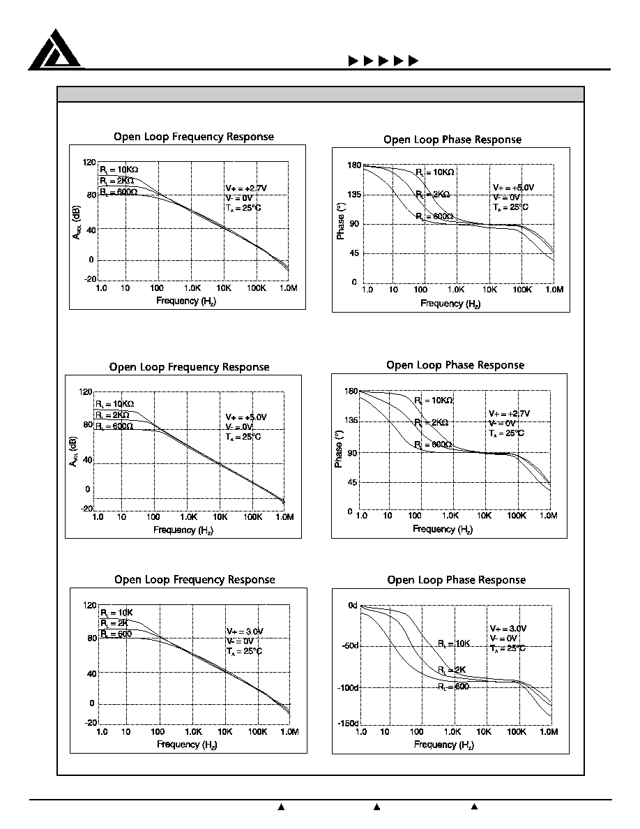
TYPICAL PERFORMANCE CHARACTERISTICS

©2000 California Micro Devices Corp. All rights reserved.
2/00
215 Topaz Street, Milpitas, California 95035 Tel: (408) 263-3214 Fax: (408) 263-7846 www.calmicro.com
6
CALIFORNIA MICRO DEVICES
CMC7101A
TYPICAL PERFORMANCE CHARACTERISTICS

7
© 2000 California Micro Devices Corp. All rights reserved.
2/00
215 Topaz Street, Milpitas, California 95035 Tel: (408) 263-3214 Fax: (408) 263-7846 www.calmicro.com
CALIFORNIA MICRO DEVICES
CMC7101A
TYPICAL PERFORMANCE CHARACTERISTICS

©2000 California Micro Devices Corp. All rights reserved.
2/00
215 Topaz Street, Milpitas, California 95035 Tel: (408) 263-3214 Fax: (408) 263-7846 www.calmicro.com
8
CALIFORNIA MICRO DEVICES
CMC7101A
2.0 Input Common Mode Range and Output
Voltage Considerations
The CMC7101A is capable of accommodating input
common mode and output voltages equal to both
power supply rails. Nor will voltages that exceed the
supply voltages cause phase inversion of the output.
However, ESD diode clamps are provided at the inputs
that can be damaged if static currents in excess of ± 5
mA are allowed to flow through them. This can occur
when the magnitude of input voltage exceeds the rail
by more than 0.3 volt. To preclude damage, an current
limiting resistor, R
s
, in series with the input is
recommended as illustrated in Figure 1 whose value
for R
s
is given by:
Vin - (V+ + 0.3 V)
R
s
>
5 mA
For V+ (or V-) equal to 2.7 volts and Vin equal to
10 volts, Rs should be chosen for a value of 1.5 K
or greater.
2.1 Output Current and Power Dissipation
Considerations
The CMC7101A is capable of sinking and sourcing
output currents in excess of 75 mA at voltages very
nearly equal to the rails. As such, it does not have any
internal short circuit protection (which would in any
event detract from its rail to rail capability). Accordingly,
power dissipation and junction temperature should be
considered in any application.
Obviously, the worst case from a power dissipation
point of view is when the output is shorted to either
ground in a single rail application or to the opposite
supply voltage in split rail applications. Since this device
only draws 300 micro Amps supply current, its
contribution to the junction temperature, T
J
, is
negligible. As an example, let us analyze a situation in
Application Trouble Shooting
(1)
Figure 1 R
S
Input Current Protection
Application Benefits
1.0 Packaging
Most of the benefits of the CMC7101A are due to the use of
a SOT package. The industry has readily adopted the SMT
package technique and a SOT23-5 footprint is an easy way
to save space. This leads to smaller finished products.
PC CARDS (PCMCIA type III cards) require low profile
components. At 0.056 inches (1.43 mm), the CMC7101A
is ideal.
1.1 Signal Integrity
As products become smaller, the natural space used to
isolate circuits is lost. Signals can interact or pick up
noise in these designs. By using a physically smaller
amplifier package, the CMC7101A can be placed closer
to the signal source, reducing noise pickup, and its small
size makes it a simple buffer.
Rail to Rail Inputs and Output allow the amplifier to
operate from lower supplies and also maintain signal
level swings under large signal amplitude conditions.
1.2 Simplified Board Layout
Board layout is helped in a couple of ways due to the
small size. Op Amps can be placed where amps are
needed, shortening signal paths and PCB traces subject
to noise pick up. Compared to a dual or quad device,
two or four strategically placed SOT AMPs reduce cross-
talk and avoid long PC wiring traces.
1.3 Lower Distortion
The CMC7101A has lower distortion than other SOT
Amps, which combined with the high open loop gain
allows it to achieve very low audio signal distortion.
1.4 Lower Power Supply Current Drain
The CMC7101A has lower power supply drain than other
SOT Amps, making the part an instant upgrade to
industry standard 7101 applications. Lower supply
current means longer operation in battery operated
products, and simpler power supply regulator or
converter designs when many amplifiers are used in one
system.
1.5 Higher Output Drive
The CMC7101A has higher output current than other
SOT Amps, making the part an instant upgrade to industry
standard 7101 applications. Higher output current
means that existing circuits can start up sooner when
power is applied (due to output current charging load
capacitance), a feature needed when sections of a system
are powered down frequently to save power or reduce
cross-talk, such as a cellular handset.

9
© 2000 California Micro Devices Corp. All rights reserved.
2/00
215 Topaz Street, Milpitas, California 95035 Tel: (408) 263-3214 Fax: (408) 263-7846 www.calmicro.com
CALIFORNIA MICRO DEVICES
CMC7101A
Since the parasitic capacitance can change between
the breadboard and the production printed circuit board,
we favor the use of a gimmick , a technique perfected
by TV technicians in the 1950s. A gimmick is made
by taking two lengths (typically about a foot) of small
gauge insulated wire such as AWG 24, twisting them
together, and then after baring all ends soldering the
gimmick across R
f
. With the circuit operating, C
f
is
adjusted by clipping short lengths of the gimmick
off until the compensation is nominal. Then simply
remove the gimmick, take it to an impedance bridge,
and select the capacitor accordingly.
Figure 2 C
F
High Frequency Compensation
2.3 Capacitive Load Considerations
The CMC7101A is capable of driving capacitive loads
in excess of 100 pF without oscillation. However,
significant peaking will result. Probably the easiest way
to minimize this problem is to use an isolation resistor
as shown in Figure 3.
Figure 3 Riso Capacitive Load Isolation
2.4 Power Supply Decoupling
The CMC7101A is not prone to oscillation without the
use of power supply decoupling capacitors, however to
minimize hum and noise pick-up, it is recommended
that the rails be bypassed with 0.01 micro farad capacitors.
which the CMC7101A is operated from a +5 volt
supply, the output is programmed to positive
saturation, and the output pin is indefinitely shorted to
the opposite rail. In general:
P
diss
= (V+ Vout) * Iout
Where: P
diss
= Power dissipated by the chip
V+ = Supply voltage
Vout = The output voltage
In this example, V+ Vout would equal 2.5 V (-2.5
V) = 5 V, and power dissipation would be equal to
375 mW.
T
J
= T
A
+
JA
* P
diss
Where: T
A
= The ambient temperature
JA
= The thermal impedance of the package
junction to ambient
The SOT23 exhibits a
JA
equal to 325 ∞C/W. Thus for
our example the junction temperature rise would be
about 122∞C which is nearly a destructive situation
since the maximum junction temperature rating is 150
∞C. Under normal operating conditions with a resistive
load, equations (2) and (3) may be used to determine
T
J .
For example, for Vout = 1.35 volts, V+ = 2.7
volts, V- = ground, and a load of 20 mA, P
diss
= 27
mW with a corresponding junction temperature rise
of a mere 9 ∞C. If the ambient temperature is 85 ∞C
maximum, the junction temperature is a safe 94 ∞C.
2.2 Input Impedance Considerations
The CMC7101A exhibits an input impedance typically
in excess of 1 Tera (1 X 10
12
ohms) making it very
appropriate for applications involving high source
impedance such as photodiodes and high output
impedance transducers or long time constant
integrators. High source impedances usually dictate
large feedback resistors. But, the output capacitance
of the source in parallel with the input capacitance of
the CMC7101A (which is typically 3 pF) creates a
parasitic pole with the feedback resistor which erodes
the phase margin of the amplifier. The usual fix is to
bypass, R
f
, as shown in Figure 2 with a small capacitor
to cancel the input pole. The usual formula for
calculating C
f
always results in a value larger than
required:
1 1
>
2
R
S
C
S
2
R
f
C
f
(2)
(4)
(3)

©2000 California Micro Devices Corp. All rights reserved.
2/00
215 Topaz Street, Milpitas, California 95035 Tel: (408) 263-3214 Fax: (408) 263-7846 www.calmicro.com
10
CALIFORNIA MICRO DEVICES
CMC7101A
TAPE AND REEL SPECIFICATIONS
CMC7101A Benefits
3.0 High Side Current Sense
To monitor a load current it is necessary to insert a
current sense resistor in the power supply feed, as shown
in figure 4. The resulting voltage drop is proportional
to the load current, but as both ends of this resistor are
at (or very near to) the supply voltage, it is difficult to
use a conventional Op Amp.
The CMC7101A is ideal for this application as the inputs
can operate at either supply rail (or at ground when
used with a single supply). The output voltage is directly
proportional to current in the load, scaled by the gain
of the amplifier.
To reduce the power loss in the sense resistor and also
keep the supply voltage to the load immune to load
current variations, a small value Rsense is used.
An excellent application for this circuit is in a battery
charger, where the charging current is monitored to
detect end of charge (battery current will rise as the
cells top off), and charging must be reduced to prevent
damage (out gassing or over heating).
The sense resistor can be placed in the negative side
(known as Low Side Sensing), however this is less desirable
due to disruption of the ground path.
3.1 Rail To Rail Output Swing
Making smaller and lighter products requires the reduction
of battery size, lowering of battery voltage, or both. The
lower voltage products have less headroom, for a given
signal swing, and this demands better amplifier
performance. Rail To Rail Outputs help maintain the
existing signal level when products are redesigned for
lower voltage supplies.
3.2 Rail to Rail input Swing
When the amplifier is used as a buffer, the input of the
amplifier follows the input signal and if this is large
compared to the available supply voltage, it is important
that the Op Amp has a wide CMVR (Common Mode
Voltage Range). RRIO Op Amps have a CMVR equal (or
greater than) the supplies and this allows large signal
swings without clipping or distortion.
Figure 4 High Side Current Sense circuit
CMC7101A Physical Dimensions
For a complete mechanical drawing refer to http://www.calmicro.com/prod/data/package/sot-23.htm.