Äîêóìåíòàöèÿ è îïèñàíèÿ www.docs.chipfind.ru
3/5/2001
1
215 Topaz Street, Milpitas, California 95035
Tel: (408) 263-3214 Fax: (408) 263-7846 www.calmicro.com
CMPWR130
CALIFORNIA MICRO DEVICES
© 2001 California Micro Devices Corp. All rights reserved. SmartORTM is a trademark of California Micro Devices Corp
300mA SmartOR
TM
Regulator with V
AUX
Drive
Features
· Automatic detection of V
CC
input supply
· Glitch-free output during supply transitions
· Built-in hysteresis during supply selection
· 300mA output maximum load current
· Overload current protection
· Short circuit current protection
· Operates from either V
CC
or V
OUT
· 8-pin SOIC package
Product Description
The SmartOR
TM
CMPWR130 is a low dropout regulator
that delivers up to 300mA of load current at a fixed 3.3V
output. An internal threshold level (TYP 4.1V) is used to
prevent the regulator from being operated below dropout
voltage. The device continuously monitors the input
supply and will automatically disable the regulator when
V
CC
falls below the threshold level. When the regulator is
disabled, the control signal "Drive" (Active Low) is
enabled, which allows an external PMOS switch to
power the load from an auxiliary 3.3V supply.
Applications
· PCI adapter cards
· Network Interface Cards (NIC's)
· Dual power systems
· Systems with standby capabilities
C1670101
When V
CC
is restored to a level above the select thresh-
old, the control signal for the external PMOS switch is
disabled and the regulator is once again enabled.
All the necessary control circuitry needed to provide a
smooth and automatic transition between the supplies
has been incorporated. This allows V
CC
to be dynamically
switched without loss of output voltage.
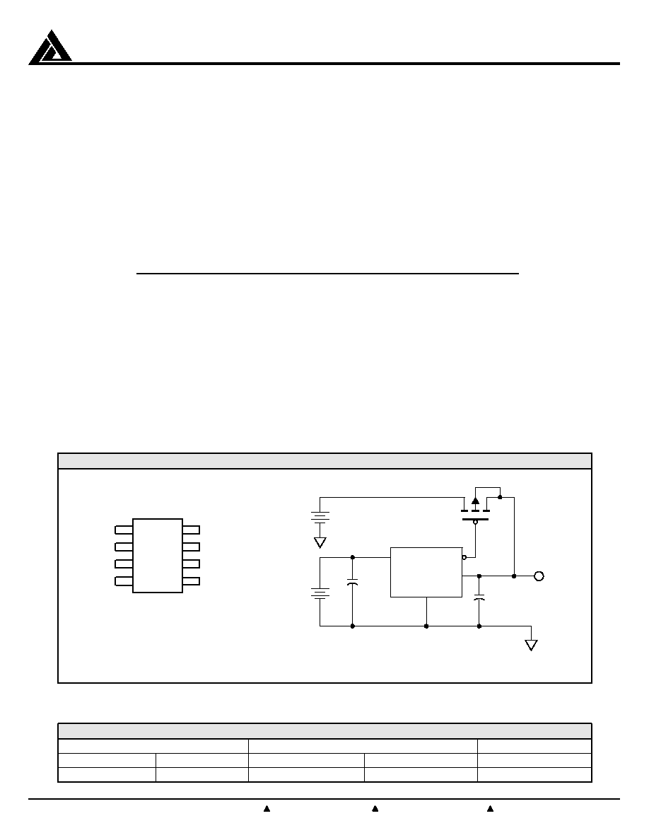
PIN DIAGRAM AND APPLICATION CIRCUIT
Pin Diagram
NC
Top View
CMPWR130
8-Pin SOIC
GND
5
4
V
OUT
NC
6
3
V
OUT
NC
7
2
DRIVE
V
CC
8
1
STANDARD PART ORDERING INFORMATION
Package
Ordering Part Number
Pins
Style
Tubes
Tape & Reel
Part Marking
8
SOIC
CMPWR130S/T CMPWR130S/R CMPWR130S
V
CC
V
CC
5V
GND
GND
DRIVE
MGSF1PO2ELT1
V
OUT
V
OUT
3.3V
300mA
CMPWR130
V
AUX
3.3V
4µF
GND
+
C
IN
1µF
C
OUT
+
+
+
Typical Application Circuit
3/5/2001
215 Topaz Street, Milpitas, California 95035
Tel: (408) 263-3214 Fax: (408) 263-7846 www.calmicro.com
2
CMPWR130
CALIFORNIA MICRO DEVICES
© 2001 California Micro Devices Corp. All rights reserved. SmartORTM is a trademark of California Micro Devices Corp
ABSOLUTE MAXIMUM RATINGS
Parameter
Rating
Unit
ESD Protection (HBM)
2000
V
V
CC,
V
OUT
Voltages
6.0, GND 0.5 V
Drive Logic Voltage
V
CC
+ 0.5, GND 0.5 V
Temperature: Storage
40 to 150
°
C
Operating Ambient
0 to 70
°
C
Operating Junction
0 to 125
°
C
Power Dissipation
(Note 1)
0.6
W
OPERATING CONDITIONS
Parameter
Range
Unit
V
CC
5 ± 0.5
V
Temperature (Ambient)
0 to 70
°
C
Load Current
0 to 300
mA
C
EXT
4.7 ± 20%
µF
ELECTRICAL OPERATING CHARACTERISTICS
(over operating conditions unless specified otherwise)
Symbol
Parameter
Conditions
MIN
TYP
MAX
UNIT
V
OUT
Regulator Output Voltage
0mA < I
LOAD
< 300mA
3.10
3.30
3.50
V
V
CCSEL
Select Voltage
Regulator Enabled
4.30
4.45
V
V
CCDES
Deselect
Voltage
Regulator Disabled
3.90 4.10
V
V
CCHYST
Hysteresis
Voltage
Hysteresis
(Note 2)
0.20
V
I
S/C
Short Circuit Output Current
V
CC
= 5V, V
OUT
= 0V
310
mA
I
RCC
V
CC
Pin Reverse Leakage
V
OUT
= 3.3V, V
CC
= 0V
2
50
µA
V
R LOAD
Load Regulation
V
CC
= 5V,
I
LOAD
= 30 to 300mA
50
mV
V
R LINE
Line
Regulation
V
CC
= 4.5V to 5.5V,
I
LOAD
= 5mA
50
mV
ICC
Quiescent Supply Current
V
CC
> V
CCSEL
, I
LOAD
= 0mA
0.6
0.8
mA
V
CCDES
> V
CC
> V
OUT
0.2
mA
V
OUT
> V
CC
0.01
0.02
mA
I
GND
Ground
Current
(Note 3)
V
CCSEL
>
V
CC
(Regulator Disabled)
0.2 0.4 mA
V
CC
= 5V,
I
LOAD
= 5mA
0.6
0.8
mA
V
CC
= 5V,
I
LOAD
= 300mA
0.7
1.4
mA
R
OH
Drive
Pull-up
Resistance
R
PULLUP
to V
CC,
V
CC
> V
CCSEL
4.0
8.0 k
R
OL
Drive
Pull-down
Resistance
R
PULLDOWN
to GND, V
CCDES
> V
CC
0.1 0.4 k
Note 1: The power rating is based on a printed circuit board heat spreading capability equivalent to 2 square inches of copper connected to
the GND pins. Typical multilayer boards using power plane construction will provide this heat spreading ability without the need for
additional dedicated copper area. (Please consult with factory for thermal evaluation assistance.)
Note 2: The hysteresis defines the maximum level of acceptable disturbance on V
CC
during switching. It is recommended that the V
CC
source impedance be kept below 0.25
to ensure the switching disturbance remains below the hysteresis during select/deselect
transitions. An input capacitor may be required to help minimize the switching transient.
Note 3: Ground pin current consists of controller current (0.15mA) and regulator current if enabled. The controller always draws 0.15mA
from either V
CC
or V
OUT
, whichever is greater. All regulator current is supplied exclusively from V
CC
. At high load currents a small
increase occurs due to current limit protection circuitry.
3/5/2001
3
215 Topaz Street, Milpitas, California 95035
Tel: (408) 263-3214 Fax: (408) 263-7846 www.calmicro.com
CMPWR130
CALIFORNIA MICRO DEVICES
© 2001 California Micro Devices Corp. All rights reserved. SmartORTM is a trademark of California Micro Devices Corp
Interface Signals
V
CC
is the power source for the internal regulator and is
monitored continuously by an internal controller circuit.
Whenever V
CC
exceeds V
CCSEL
(4.30V TYP), the internal
regulator (300mA MAX) will be enabled and deliver a
fixed 3.3V at V
OUT
. When V
CC
falls below V
CCDES
(4.10V
TYP) the regulator will be disabled.
Internal loading on this pin is typically 0.6mA when the
regulator is enabled, which reduces to 0.2mA whenever
the regulator is disabled. If V
CC
falls below the voltage on
the V
OUT
pin the V
CC
loading will further reduce to only a
few microamperes.
During a V
CC
power up sequence, there will be an
effective step increase in V
CC
line current when the
regulator is enabled. The amplitude of this step increase
will depend on the DC load current and any necessary
current required for charging/discharging the load
capacitance. This line current transient will cause a
voltage disturbance at the V
CC
pin. The magnitude of the
disturbance will be directly proportional to the effective
power supply source impedance being delivered to the
V
CC
input.
To prevent chatter during Select and Deselect transi-
tions, a built-in hysteresis voltage of 200mV has been
incorporated. It is recommended that the power supply
connected to the V
CC
input should have a source resis-
tance of less than 0.25
to minimize the event of chatter
during the enabling/disabling of the regulator.
An input filter capacitor in close proximity to the V
CC
pin
will reduce the effective source impedance and help
minimize any disturbances. If the V
CC
pin is within a few
inches of the main input filter, a capacitor may not be
necessary. Otherwise an input filter capacitor in the
range of 1µF to 10µF will ensure adequate filtering.
GND is the negative reference for all voltages. This
current that flows in the ground connection is very low
(TYP 550µA) and has minimal variation over all load
conditions.
V
OUT
is the regulator output voltage connection used to
power the load. An output capacitor of 4.7µF is used to
provide the necessary phase compensation, thereby
preventing oscillation. The capacitor also helps to
minimize the peak output disturbance during power
supply changeover.
When V
CC
falls below V
OUT
, then V
OUT
will be used to
provide the necessary quiescent current for the internal
reference circuits. This ensures excellent start-up
characteristics for the regulator.
DRIVE is an active LOW logic output intended to be
used as the control signal for driving an external PFET
whenever the regulator is disabled. This will allow the
voltage at V
OUT
to be powered from an auxiliary supply
voltage (3.3V).
The Drive pin is pulled HIGH to V
CC
whenever the
regulator is enabled, this ensures the auxiliary remains
isolated during normal regulator operation.
The output current sinking ability of this logic signal is
equivalent to a 100W resistor. The current sourcing
ability is equivalent to a 4k
resistor.
NC pins are electrically isolated from the internal
circuitry. These pins can be connected to any external
voltage level without impacting the device functionality.
PIN FUNCTIONS
Pin
Symbol
Description
1
V
CC
Positive (5V) supply input for regulator. (V
CC
> V
CCSEL
)
6,
7
V
OUT
Continuous output voltage (3.3V) is derived from either the internal regulator or low impedance
switch connected to the auxiliary supply input.
8
DRIVE
Output drive signal to control external MOSFET switch
4
GND
Negative reference for all voltages
2, 3, 5
NC
Unconnected pin which is electrically isolated from internal circuitry.
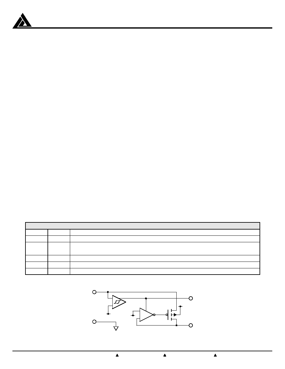
V
OUT
3.3V
300mA
V
REF
3.3V
+
V
CC
+
V
DESELECT
4.1V
GND
DRIVE
ENABLE
Simplified Electrical Schematic
3/5/2001
215 Topaz Street, Milpitas, California 95035
Tel: (408) 263-3214 Fax: (408) 263-7846 www.calmicro.com
4
CMPWR130
CALIFORNIA MICRO DEVICES
© 2001 California Micro Devices Corp. All rights reserved. SmartORTM is a trademark of California Micro Devices Corp
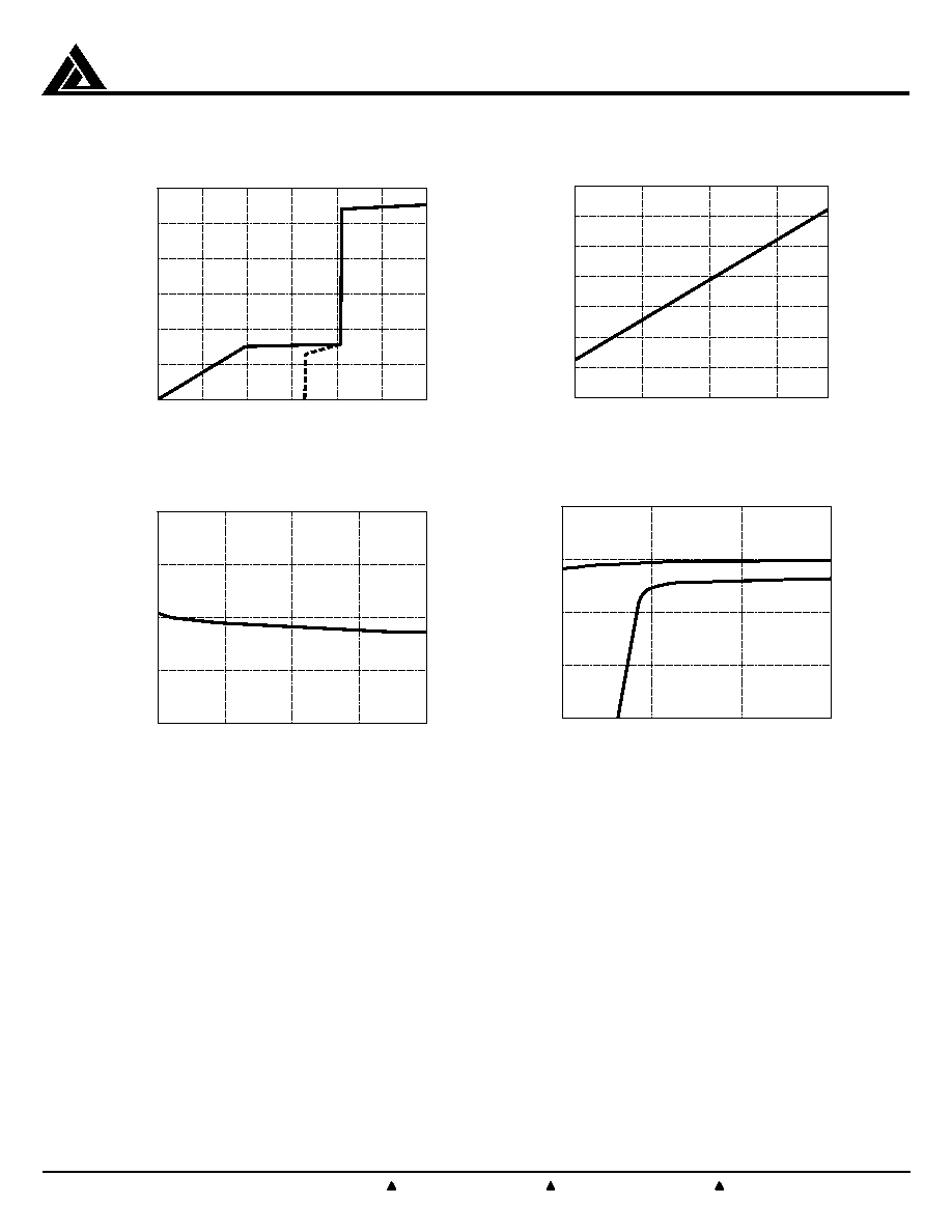
Typical DC Characteristics (nominal conditions unless specified otherwise)
0
100
200
300
400
500
600
0
1.0
2.0
3.0
4.0
5.0
6.0
V
CC
(V)
V
AUX
= 3.3V
V
AUX
= 0V
Suppl
y Current (µA)
Figure 1. Supply Current vs Voltage (V
AUX
= 3.3V)
520
540
560
580
600
620
640
660
0
100
200
300
Load Current (mA)
Gr
ound Current (µA)
Figure 2. Ground Current vs Output Load
Figure 3. Load Regulation
Figure 4. Line Regulation
3.20
3.25
3.30
3.35
3.40
0
100
200
300
400
Load Current (mA)
V
OUT
(V)
3.15
3.20
3.25
3.30
3.35
3.5
4.0
4.5
5.0
V
CC
(V)
5mA Load
300mA Load
V
OUT
(V)
3/5/2001
5
215 Topaz Street, Milpitas, California 95035
Tel: (408) 263-3214 Fax: (408) 263-7846 www.calmicro.com
CMPWR130
CALIFORNIA MICRO DEVICES
© 2001 California Micro Devices Corp. All rights reserved. SmartORTM is a trademark of California Micro Devices Corp
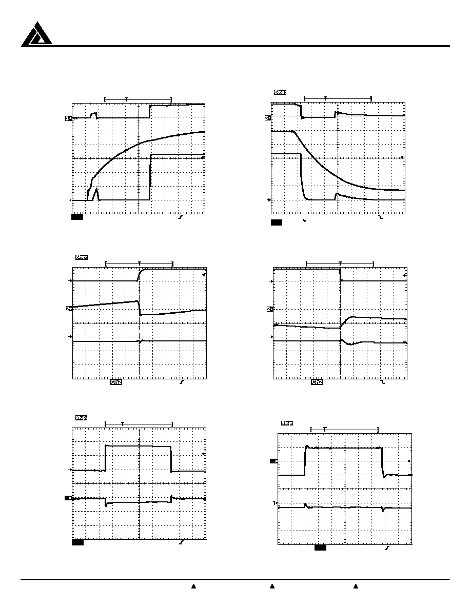
3.06V
Drive
(300mA Load)
V
CC
V
OUT
M 1ms
1V
Ch1
Ch2
5V
2
Ch3
1V
Tek Run: 50kS/s
Sample
Ch2
Typical Transient Characteristics (Supply source resistance set to 0.2
)
Figure 5. V
CC
Cold Start Power UP (V
AUX
= 0V)
Figure 6. V
CC
Complete Power Down (V
AUX
= 0V)
Figure 8. V
CC
Power Down (V
AUX
= 3.3V)
Figure 7. V
CC
Power UP (V
AUX
= 3.3V)
Figure 10. Line Transient (1V
pp
) Step Response
Figure 9. Load Transient (10% to 90%)
Step Response
3.06V
Drive
(300mA Load)
V
CC
V
OUT
M 1ms
1V
5V
2
Ch3
Ch1
Ch2
1V
50kS/s
Tek 1
Acqs
Ch2
2.32V
V
CC
(offset = 4.2V)
Drive
V
OUT
(offset = 3.3V)
(300mA Load)
M 10µs
100mV
Ch1
5V
3
1
Ch3
2V
2.5MS/s
Tek
5 Acqs
Ch3
2.1V
V
CC
(offset = 4.2V)
Drive
V
OUT
(offset = 3.3V)
(300mA Load)
M 20µs
100mV
Ch1
5V
Ch3
3
1
100mV
Teck Run: 2.5MS/s Sample
Ch3
Ch2
2.32V
Load
275mA
25mA
V
OUT
(offset = 3.3V)
M 10µs
100mV
Ch1
1
2
2V
5MS/s
Tek 3
Acqs
Ch2
5V
V
CC
V
OUT
(offset = 3.3V)
M 100µs
20mV
Ch2
Ch1
500mV
500kS/s
Tek 2
Acqs
Ch2
4.5V
5.5V
2