Äîêóìåíòàöèÿ è îïèñàíèÿ www.docs.chipfind.ru
CALIFORNIA MICRO DEVICES
©2000 California Micro Devices Corp. All rights reserved. SmartORTM is a trademark of California Micro Devices Corporation.
12/5/2000
1
215 Topaz Street, Milpitas, California 95035
Tel: (408) 263-3214 Fax: (408) 263-7846 www.calmicro.com
CMPWR160
USB Peripheral Power Management
Features
· 3.3V regulated output up to 500mA
· Quiescent current 35µA (typical)
· Shutdown mode current 7µA (typical)
· 30ms active LOW Power-On Reset (POR) pulse
· Thermal overload protection
· Foldback current limiting protection
· Reverse-current protection
· 8 pin SOIC power package
Applications
· Bus-powered USB peripherals
· Self-powered USB peripherals
· Portable/battery-powered devices
· Critical power monitoring, hot-insertion devices
C1571000
1
2
3
4
V
CC
SD
POR
V
OUT
8
7
6
5
GND
GND
GND
GND
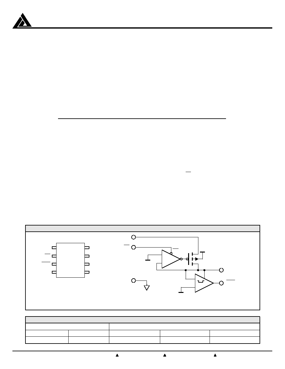
Top View
CMPWR160
8 LEAD SOIC
V
OUT
3.3V/500mA
POR
V
REF
3.3V
+
V
CC
SD
2.9V
GND
+
30ms
SD
Pin Diagram
Simplified Electrical Schematic
Standard Part Ordering Information
Package
Ordering Part Number
Pin
Style
Tubes
Tape & Reel
Part Marking
8
Power
SOIC CMPWR160SA/T
CMPWR160SA/R CMPWR160SA
The SmartOR
TM
CMPWR160 combines a Low Dropout
Regulator (LDO) with a Power-On Reset (POR) pulse
generator, and is intended for Universal Serial Bus
(USB) peripherals. To meet the specification require-
ments of both USB 1.0 and USB 2.0, the CMPWR160
draws a very low quiescent current (35µA), and delivers
up to 500mA of load current at a fixed 3.3V output.
The POR pulse (active LOW) has a typical duration of
30ms after the output has exceeded and stabilized
above 2.9V. Thus a new POR pulse is developed each
time the regulator power is interrupted and restored,
which occurs often on USB buses when cables are
connected (or disconnected) by the user. It is not
necessary to have a V
CC
supply for POR to operate,
allowing the CMPWR160 to work in Wired-ORed power
systems.
When V
CC
is powered down, the device will automatically
enter reverse-current protection mode and maintain
isolation between V
OUT
and V
CC
. This is useful for applica-
tions that can use power from the USB port in addition to
internal batteries or an AC adapter supply (Wired-ORed
power systems). In the event of V
CC
collapsing below
V
OUT
, the device will automatically enter shutdown mode
and fully isolate the V
CC
power source from the output.
A ShutDown input (SD) forces the regulator to be
powered down on demand. While in shutdown mode the
POR circuitry will remain active, making the device
suitable for systems which contain backup or alternative
power sources.
The CMPWR160 is available in an 8-pin SOIC thermally
enhanced package, ideal for applications where space
is tight.
Block Diagram
CALIFORNIA MICRO DEVICES
©2000 California Micro Devices Corp. All rights reserved. SmartORTM is a trademark of California Micro Devices Corporation.
12/5/2000
215 Topaz Street, Milpitas, California 95035
Tel: (408) 263-3214 Fax: (408) 263-7846 www.calmicro.com
2
CMPWR160
Operating Conditions
Parameter
Range
Unit
V
CC
4.2
to
5.5
V
Temperature (Ambient)
0 to 70
°
C
Load Current
0 to 500 mA
C
EXT
10 ± 10%
µF
Absolute Maximum Ratings
Parameter
Rating
Unit
ESD Protection (HBM)
2000
V
V
CC
/V
OUT
Voltage
6.0, GND 0.5 V
SD Logic Input Voltage
V
CC
+ 0.5, GND 0.5 V
POR Logic Output Voltage
V
OUT
+ 0.5, GND 0.5
V
Temperature: Storage
40 to 150
Operating Ambient
0 to 70
°
C
Operating Junction
0 to 125
Power Dissipation
Note 1
Internally
Limited
Electrical Operating Characteristics
(over operating conditions unless specified otherwise)
Symbol
Parameter
Conditions
MIN
TYP
MAX
UNIT
V
OUT
Regulator Output Voltage
0mA < I
LOAD
< 500mA
3.135
3.30
3.465
V
I
LIM
Regulator
Current
Limit
550
mA
I
S/C
Short-Circuit Current Limit
300
mA
V
R LOAD
Load
Regulation
V
CC
= 5V, I
LOAD
= 5mA to 500mA
75
mV
V
R LINE
Line
Regulation
V
CC
= 4.2V to 5.5V, I
LOAD
= 5mA
2
mV
V
DO
Regulator
Dropout
Voltage
MIN V
CC
V
OUT
for I
LOAD
= 500mA
0.6 0.9 V
I
Q
Quiescent Supply Current
Regulator Enabled (No Load)
35
50
µA
I
SD
Shutdown Supply Current
Regulator Disabled
7
10
µA
I
RCC
V
CC
Pin Reverse Leakage
V
OUT
= 3.3V, V
CC
= 0V
1
10
µA
V
IH SD
Shutdown
High
Detect
V
CC
= 5V
3.0
V
V
IL SD
Shutdown
Low
Detect
V
CC
= 5V
1.0
V
V
POR
POR Detect Threshold
4.2V < V
CC
< 5.5V
2.8
2.9
3.0
V
T
POR
POR
Pulse
Duration
20
30
40
ms
R
POR
POR
Output
Impedance After POR Threshold Detected
0.2 0.5 2 k
Sinking to GND/Sourcing from V
CC
T
DISABLE
Shutdown
Temperature
160
°
C
T
HYST
Thermal
Hysteresis
20
°
C
Note 1: The SOIC package used is thermally enhanced through the use of a fused integral leadframe. The power rating is based on a printed
circuit board heat spreading capability equivalent to 2 square inches of copper connected to the GND pins. Typical multi-layer boards
using power plane construction will provide this heat spreading ability without the need for additional dedicated copper area. (Please
consult with factory for thermal evaluation assistance.)
CALIFORNIA MICRO DEVICES
©2000 California Micro Devices Corp. All rights reserved. SmartORTM is a trademark of California Micro Devices Corporation.
12/5/2000
3
215 Topaz Street, Milpitas, California 95035
Tel: (408) 263-3214 Fax: (408) 263-7846 www.calmicro.com
CMPWR160
Interface Signals
V
CC
is the input power source for the Low Drop Out
Regulator, capable of delivering 3.3V/500mA output
current even when the input is as low as 4.2V.
Internal loading on this pin is typically 35µA when the
regulator is enabled, which reduces to only 7µA when-
ever the regulator is shutdown (SD taken Low). In the
event of V
CC
collapsing below V
OUT
, the loading at V
CC
will
immediately reduce to less than 0.1µA.
If the V
CC
pin is within a few inches of the main input
filter, a capacitor may not be necessary. Otherwise an
input filter capacitor in the range of 1µF to 10µF will
ensure adequate filtering.
SD is the regulator shutdown input logic signal which is
Active Low. This is a true CMOS input signal referenced
to V
CC
supply. When the pin is tied High (V
CC
) the
regulator operates fully. When the pin is taken to GND,
the device enters shutdown mode and the regulator is
fully disabled. In this mode all critical POR circuitry
remains fully powered consuming less than 7µA (typical).
V
OUT
is the regulator output voltage used to power the
load. An output capacitor of 10µF is used to provide the
necessary phase compensation, thereby preventing
oscillation. The capacitor also helps to minimize the peak
output disturbance during line or load transients. When-
ever V
CC
collapses below the output the device immedi-
ately enters reverse protection mode to prevent any
current flow back into the regulator pass transistor.
Under these conditions V
OUT
will also be used to provide
the necessary quiescent current for the internal refer-
ence and POR circuits. This ensures excellent start-up
characteristics for the regulator.
POR is the Power-On-Reset output pin (Active Low).
When V
OUT
rises above the POR threshold voltage
(typically 2.9V), the pin is forced to logic low (GND). The
pin remains logic low for 30ms then it is forced logic high
(3.3V). If V
OUT
falls below the POR threshold voltage
during this 30ms interval POR will remain logic low. If it
falls below the voltage threshold and then recovers the
30ms time will reset.
If V
OUT
falls below the POR threshold voltage POR is
immediately forced to logic low.
The power-on reset circuitry is designed to remain active
under all conditions and will produce a valid output even
when V
CC
is not present. A very low quiescent current
(7µA typical) ensures continuous operation of the POR
circuit.
GND is the negative reference for all voltages. This
current that flows in the ground connection is very low
(35µA typical with the regulator enabled and 7µA typical
with the regulator disabled).
Pin Functions
Symbol
Description
V
CC
Positive supply input for regulator. When V
CC
falls below V
OUT
the regulator is disabled.
SD
Shutdown control input signal (Active Low) to disable internal voltage regulator and current supply
to less than 7µA.
POR Power-On-Reset output signal is held Low until the output has been stable (>2.9V) for at least 30ms.
V
OUT
Regulator voltage ouput (3.3V) capable of delivering 500mA when device is enabled (SD is High).
Whenever the output exceeds 2.9V (TYP) the POR pulse is triggered.
GND
Negative reference for all voltages
V
CC
V
CC
5V
SD
GND
GND
POR
V
OUT
V
OUT
3.3V/500mA
uP Reset
CMPWR160
10µF
+
C
IN
1µF
C
OUT
+
+
Typical Application Circuit
CALIFORNIA MICRO DEVICES
©2000 California Micro Devices Corp. All rights reserved. SmartORTM is a trademark of California Micro Devices Corporation.
12/5/2000
215 Topaz Street, Milpitas, California 95035
Tel: (408) 263-3214 Fax: (408) 263-7846 www.calmicro.com
4
CMPWR160
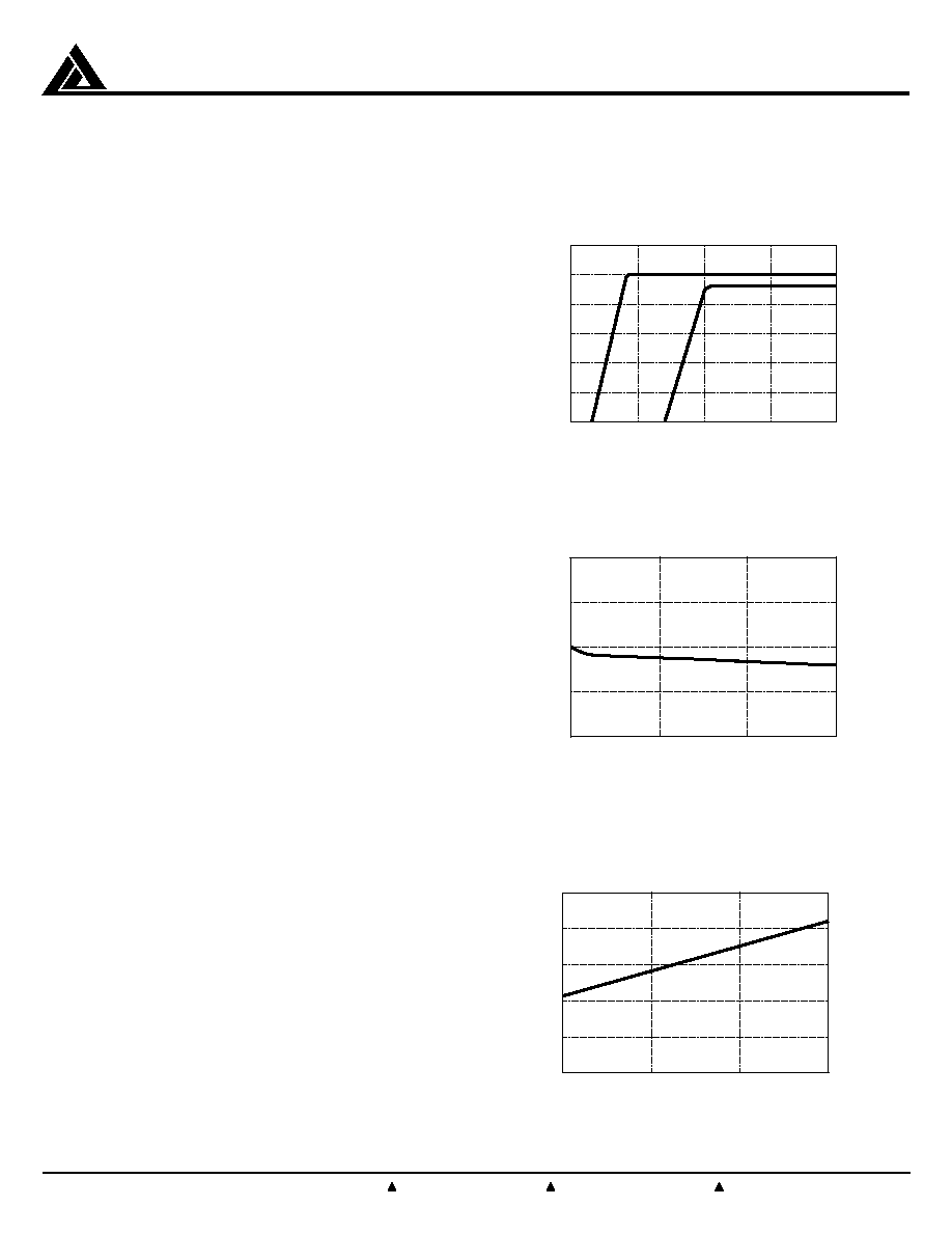
Typical DC Characteristics
Unless stated otherwise, all DC characteristics were
measured at room temperature with a nominal V
CC
supply voltage of 5V and an output capacitance of 10µF.
Resistive load conditions were used.
Line Regulation Characteristics of the regulator are
shown in Figure 1. At maximum rated load conditions
(500mA), a 100mV drop in regulation occurs when the
line voltage has collapses below 3.8V. For light load
conditions (5mA), regulation is maintained for line
voltages as low as 3.3V.
Load Regulation performance is shown from zero to
maximum rated load in Figure 2. A 10% to 100% change
of rated load, results in an output voltage change of less
than 10mV. This translates into an effective output
impedance of approximately 0.02
.
Figure 1. Line Regulation
3.05
3.10
3.15
3.20
3.25
3.30
3.35
3.0
3.5
4.0
VCC (V)
V
OUT
(V)
4.5
5mA Load
500mA Load
5.0
3.40
3.35
3.30
3.25
3.20
0
200
400
Load Current (mA)
V
OUT
(V)
600
Figure 2. Load Regulation
Ground Current is shown across the entire range of
load conditions in Figure 3. The ground current increases
by 40µA across the range of load conditions. This
increase is due to the current limiting protective circuitry
becoming active.
Figure 3. Ground Current
80
100
60
40
20
0
0
200
400
Load Current (mA)
Gr
ound Current (µA)
600
CALIFORNIA MICRO DEVICES
©2000 California Micro Devices Corp. All rights reserved. SmartORTM is a trademark of California Micro Devices Corporation.
12/5/2000
5
215 Topaz Street, Milpitas, California 95035
Tel: (408) 263-3214 Fax: (408) 263-7846 www.calmicro.com
CMPWR160
Typical DC Characteristics
continued
V
CC
Operating Current (no load, SD high) is shown
across a range of V
CC
supply voltages with the regulator
enabled in Figure 4. The graph shows that the operating
current is 35µA typical and changes by less than 1µA
across this range.
Figure 4. V
CC
Operating Current (no load)
40
50
60
30
20
10
0
3.5
4.5
5.5
V
CC
(V)
Suppl
y Current (µA)
V
CC
Shutdown Current variation with the V
CC
supply
voltage is shown in Figure 5.
8
10
6
4
2
0
1.5
2.5
3.5
V
CC
(V)
Suppl
y Current (µA)
5.5
4.5
Figure 5. V
CC
Shutdown Current