 | ÐлекÑÑоннÑй компоненÑ: CMPWR161 | СкаÑаÑÑ:  PDF PDF  ZIP ZIP |
Äîêóìåíòàöèÿ è îïèñàíèÿ www.docs.chipfind.ru
©
2004 California Micro Devices Corp. All rights reserved.
01/14/04
430 N. McCarthy Blvd., Milpitas, CA 95035-5112
L Tel: 408.263.3214
L Fax: 408.263.7846 L www.calmicro.com
1
CMPWR161
Micropower, Low Noise 4.75V/150mA LDO Regulator
Features
·
Excellent power supply ripple rejection for
V
IN
-V
OUT
down to 110mV
·
Excellent power supply ripple rejection in
audible band (20Hz to 20KHz)
·
Very low dropout voltage (110mV at 150mA)
·
Fast transient response minimizes glitches in
audible band.
·
Low noise in audible band
·
Guaranteed to deliver 150mA output at
4.75V output
·
Low quiescent current--300
µ
A
typical
·
"Zero" current shutdown mode
·
5205 compatible pin-out
·
5-lead SOT-23 package
·
Lead-free version available
Applications
·
5V analog supply for audio CODEC
·
Low noise power supply ideal for audio use
·
Notebook computers
·
Sound cards
·
Motherboards
·
Set top boxes
Product Description
The CMPWR161 is a micropower, low noise regulator
designed specifically to filter out noise from a 5V digital
supply making it ideal for noise-sensitive analog appli-
cations. The CMPWR161 delivers up to 150mA at a
fixed 4.75V output. A bandgap reference bypass pin
(BYP) provides low noise operation when an external
capacitor is connected between this pin and ground. In
addition, the CMPWR161 features an enable pin (EN)
which allows the regulator to be placed into shutdown
mode supporting low power and battery applications.
The CMOS regulator features low quiescent current
even at full load.
The CMPWR161 is housed in a 5-pin SOT-23 package,
which is ideal for space critical applications. It is avail-
able with optional lead-free finishing.
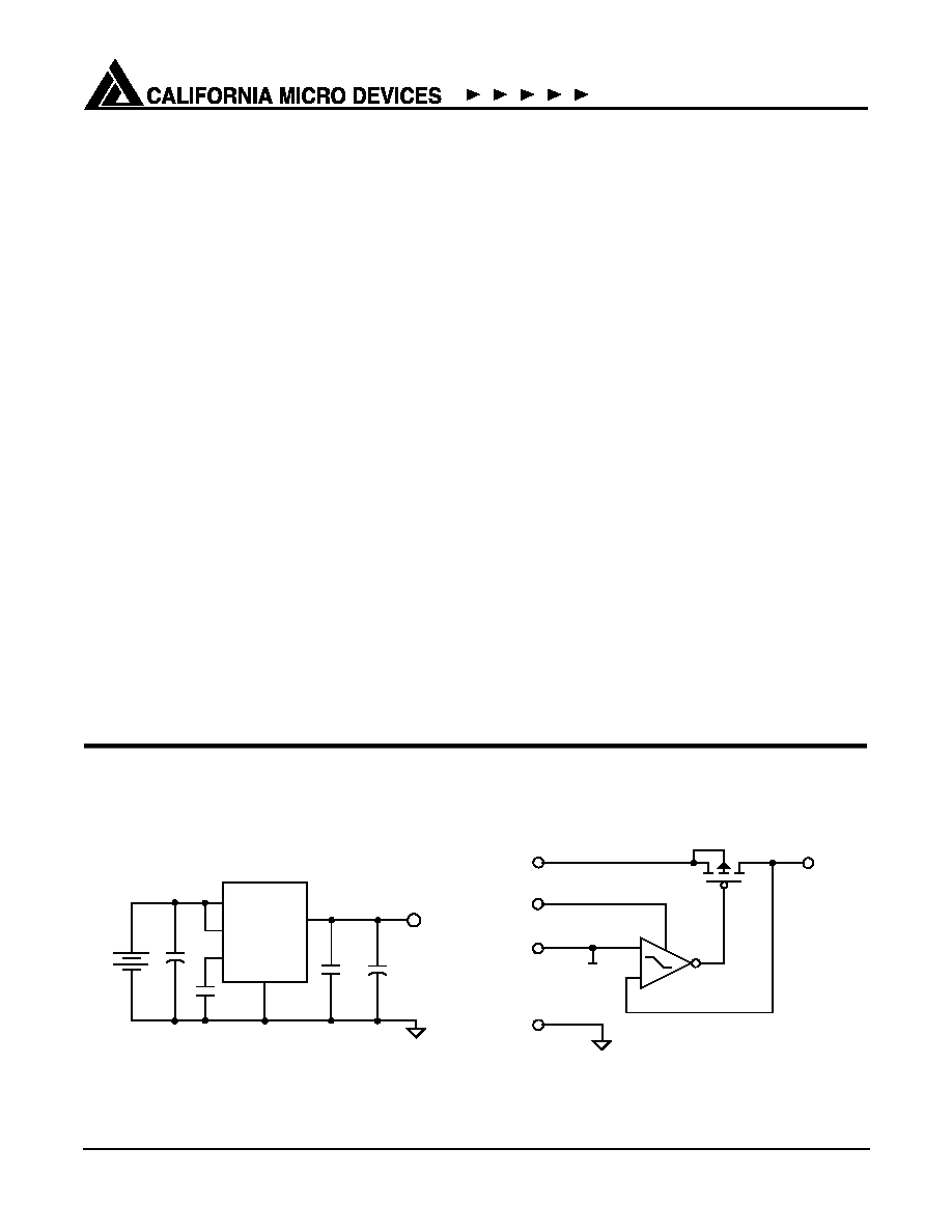
Simplified Electrical Schematic
Typical Application Circuit
EN
+
V
IN
GND
V
OUT
-
BYP
V
REF
4.75V
10kHz
V
IN
EN
V
OUT
GND
Supply
Voltage
1
µ
F
100nF
10
µ
F
+
-
V
OUT
+
+
BYP
10nF
C
OUT
C
IN
4.75V@
5V
GND
CMPWR161
150mA
©
2004 California Micro Devices Corp. All rights reserved.
2
430 N. McCarthy Blvd., Milpitas, CA 95035-5112
L Tel: 408.263.3214
L Fax: 408.263.7846 L www.calmicro.com
01/14/04
CMPWR161
Ordering Information
Note 1: Parts are shipped in Tape & Reel form unless otherwise specified.
PIN DESCRIPTIONS
PIN
NAME
DESCRIPTION
1
V
IN
Positive input voltage for the regulator. The internal loading on this input is typically 300
µA when-
ever the regulator is enabled and less than 1
µA when the regulator is disabled. If this input is
greater than 2 inches from the main input filter, a 1
µF ceramic capacitor is recommended for addi-
tional filtering.
2
GND
The negative reference for all voltages.
3
EN
Enable/shutdown input. When EN is asserted high (V
EN
2V), the regulator is enabled. When EN
is asserted low, the regulator is shutdown (V
OUT
=0V). This input is compatible with CMOS logic.
4
BYP
Reference bypass pin. This input is used to connect an external capacitor (C
BYP
) for noise reduc-
tion and to maximize power supply ripple rejection. A 10nF capacitor is recommended for this func-
tion.
5
V
OUT
The regulated voltage output. An output capacitor of 10
µF is recommended to provide the neces-
sary phase compensation for the regulator and also minimize any transient disturbances.
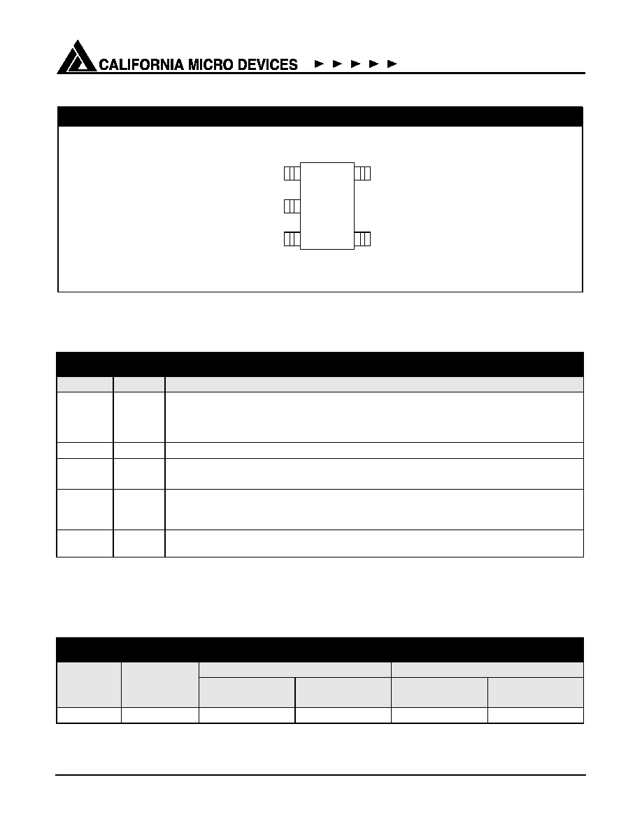
PACKAGE / PINOUT DIAGRAM
Note: This drawing is not to scale.
5-pin SOT23
V
IN
GND
EN
V
OUT
BYP
1
2
5
3
4
1
61Y/R
Top View
PART NUMBERING INFORMATION
Pins
Package
Standard Finish
Lead-free Finish
Ordering Part
Number
1
Part Marking
Ordering Part
Number
1
Part Marking
5
SOT23-5
CMPWR161Y
161Y
CMPWR161R
161R
©
2004 California Micro Devices Corp. All rights reserved.
01/14/044
430 N. McCarthy Blvd., Milpitas, CA 95035-5112
L Tel: 408.263.3214
L Fax: 408.263.7846
L www.calmicro.com
3
CMPWR161
Specifications
Note 1: Operating Characteristics are over Standard Operating Conditions unless otherwise specified.
ABSOLUTE MAXIMUM RATINGS
PARAMETER
RATING
UNITS
ESD Protection (HBM)
+2000
V
Pin Voltages
V
IN
V
OUT
V
EN
[GND - 0.5] to [+6.5]
[GND - 0.5] to [+6.5]
[GND - 0.5] to [V
CC
+0.5]
V
V
V
Storage Temperature Range
-40 to +150
°C
Operating Temperature Range
Ambient
Junction
0 to +70
0 to +125
°C
°C
STANDARD OPERATING CONDITIONS
PARAMETER
RATING
UNITS
V
IN
4.9 to 5.5
V
Ambient Operating Temperature Range
0 to +70
°C
Load Current
0 to 150
mA
C
OUT
10 +10%
µF
ELECTRICAL OPERATING CHARACTERISTICS
(SEE NOTE 1)
SYMBOL
PARAMETER
CONDITIONS
MIN
TYP
MAX
UNITS
V
OUT
Regulator Output Voltage
0mA < I
LOAD
< 150mA
4.65
4.75
4.85
V
V
R LOAD
Load Regulation
5mA < I
LOAD
< 150mA, V
IN
=5.0V
0
mV
V
R LINE
Line Regulation
xx
I
LOAD
= 5mA, 4.9V < V
CC
< to 5.5V
1
mV
V
DO
Regulator Dropout Voltage
Minimum V
IN
-
V
OUT
for I
LOAD
= 150mA
110
250
mV
I
IN
V
IN
Current
Shutdown (Regulator Disabled), V
OUT
tied to GND
0.01
10
µA
I
GND
Ground Current
Regulator Enabled, I
LOAD
= 0mA
300
500
µA
Regulator Enabled, I
LOAD
= 150mA
300
500
µA
R
REJ
Ripple Rejection
V
IN
-
V
OUT
= 150mV, I
LOAD
= 150mA,
C
BYP
= 10nF
=100Hz
=10kHz
x
x
42
25
x
x
dB
dB
V
IH
EN Input Logic High Threshold
2.0
V
V
IL
EN Input Logic Low Threshold
0.5
V
©
2004 California Micro Devices Corp. All rights reserved.
4
430 N. McCarthy Blvd., Milpitas, CA 95035-5112
L Tel: 408.263.3214
L Fax: 408.263.7846 L www.calmicro.com
01/14/04
CMPWR161
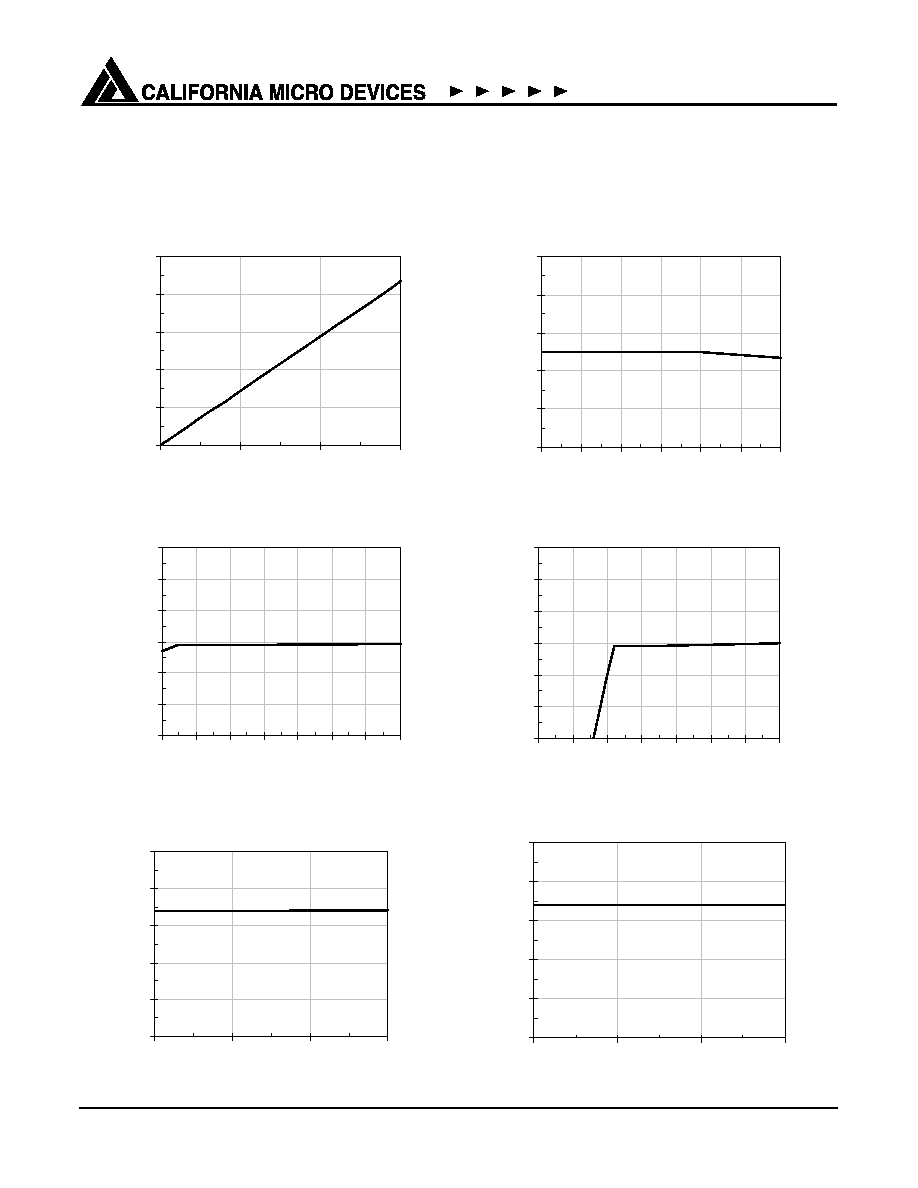
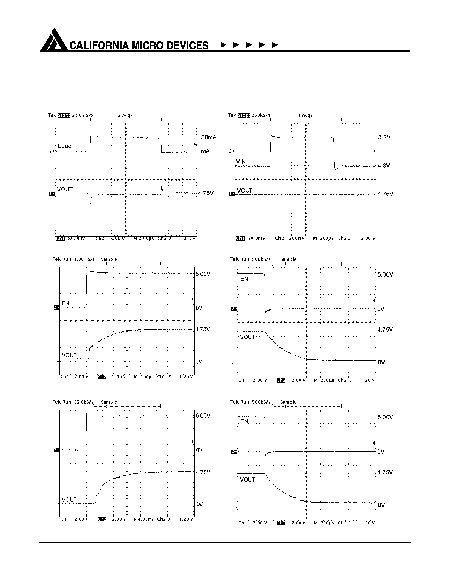
Performance Information
CMPWR161 Typical DC Characteristics (nominal conditions unless specified otherwise)
Nominal Conditions: C
IN
=10
µF & 0.1µF, C
OUT
=10
µF & 0.1µF, C
BYP
=0.01
µF, V
IN
=5.0V, I
LOAD
=5mA.
Dropout Voltage vs. Load (V
OUT
=4.70V)
0
25
50
75
100
125
0
50
100
150
Load Current [mA]
Dropout [mV]
Load Regulation
4.70
4.72
4.74
4.76
4.78
4.80
0
50
100
150
200
250
300
Load Current [mA]
Output Voltage [V]
Line Regulation (5mA Load)
4.72
4.73
4.74
4.75
4.76
4.77
4.78
4.75 4.80 4.85 4.90 4.95 5.00 5.05 5.10
Supply Voltage [V]
Output Voltage [V]
Line Regulation (150mA Load)
4.72
4.73
4.74
4.75
4.76
4.77
4.78
4.75 4.80 4.85 4.90 4.95 5.00 5.05 5.10
Supply Voltage [V]
Output Voltage [V]
Supply Current vs. Voltage (EN = V
IN
)
0
100
200
300
400
500
4.75
5.00
5.25
5.50
Supply Voltage [V]
Supply Current [uA]
Ground Current vs. Output Load
0
100
200
300
400
500
0
50
100
150
Load Current [mA]
Ground Current [uA]
©
2004 California Micro Devices Corp. All rights reserved.
01/14/044
430 N. McCarthy Blvd., Milpitas, CA 95035-5112
L Tel: 408.263.3214
L Fax: 408.263.7846
L www.calmicro.com
5
CMPWR161
Performance Information (cont'd)
CMPWR161 Transient Characteristics (nominal conditions unless specified otherwise)
1mA-150mA Load Step (V
IN
-V
OUT
=250mV)
4.8V 5.2V Line Step (5mA Load)
Enable Response (no BYP cap)
Disable Response (no BYP cap)
Enable Response (C
BYP
= 10nF)
Disable Response (C
BYP
= 10nF)
EN
Document Outline