 | ÐлекÑÑоннÑй компоненÑ: CMPWR330 | СкаÑаÑÑ:  PDF PDF  ZIP ZIP |
Äîêóìåíòàöèÿ è îïèñàíèÿ www.docs.chipfind.ru
CALIFORNIA MICRO DEVICES
3/6/2001
1
215 Topaz Street, Milpitas, California 95035
Tel: (408) 263-3214 Fax: (408) 263-7846 www.calmicro.com
CMPWR330
©2001 California Micro Devices Corp. All rights reserved. Smart ORTM is a trademark of California Micro Devices.
400mA SmartOR
TM
Dual Regulator with V
AUX
Switch
Features
· Continuous 3.3V output from three inputs
· Complete power management solution
· V
CC
, V
SBY
regulator supplies 400mA output
· Built-in hysteresis when selecting input supplies
· Integrated switch has very low R
DS(ON)
0.25
(TYP)
· Foldback current limiting protection
· Thermal overload shutdown protection
· 8-pin power SOIC package
Product Description
The CMPWR330 is a dual input regulator with a fully
integrated V
AUX
switch capable of delivering up to
400mA continuously at 3.3V. The output power is
provided from three independent input voltage sources
on a prioritized basis. Power is always taken in priority
using the following order V
CC
, V
SBY
, and V
AUX
.
When V
CC
(5V) or V
SBY
is present, the device automati-
cally enables the regulator and produces a stable 3.3V
output at V
OUT
.
Applications
· PCI adapter cards with Wake-On-LAN
· Network Interface Cards (NICs)
· Multiple power systems
· Systems with standby capabilities
C1680101
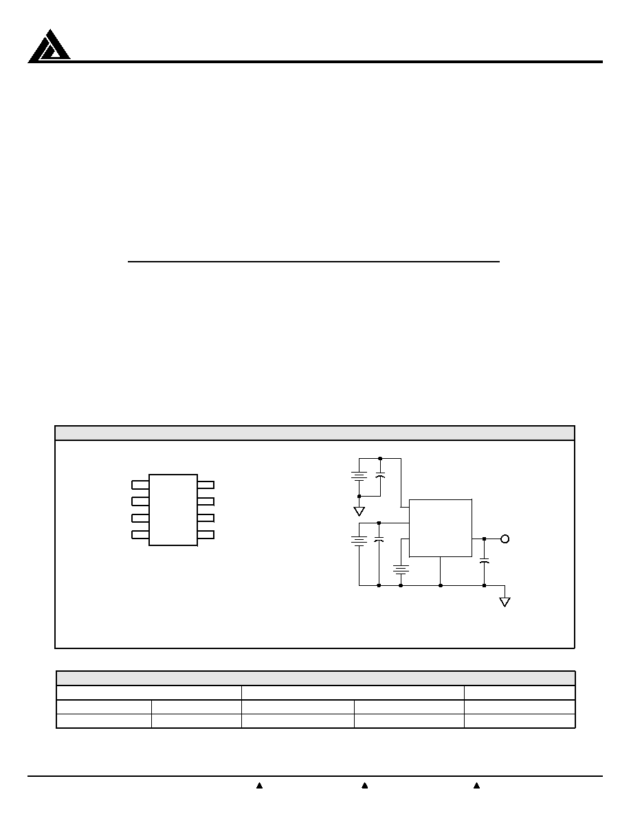
Pin Diagram
When only V
AUX
(3.3V) is present, the device provides a
low impedance direct connection (0.25
TYP) from V
AUX
to V
OUT
.
All the necessary control circuitry needed to provide a
smooth and automatic transition between all three
supplies has been incorporated. This allows the V
CC
input supply to be dynamically switched without loss of
output voltage.
PIN DIAGRAM AND ELECTRICAL SCHEMATIC
GND
Top View
CMPWR330
8-Pin Power SOIC
V
AUX
5
4
GND
V
OUT
6
3
GND
V
CC
7
2
GND
V
SBY
8
1
STANDARD PART ORDERING INFORMATION
Package
Ordering Part Number
Pins
Style
Tubes
Tape & Reel
Part Marking
8
Power
SOIC CMPWR330SA/T
CMPWR330SA/R CMPWR330SA
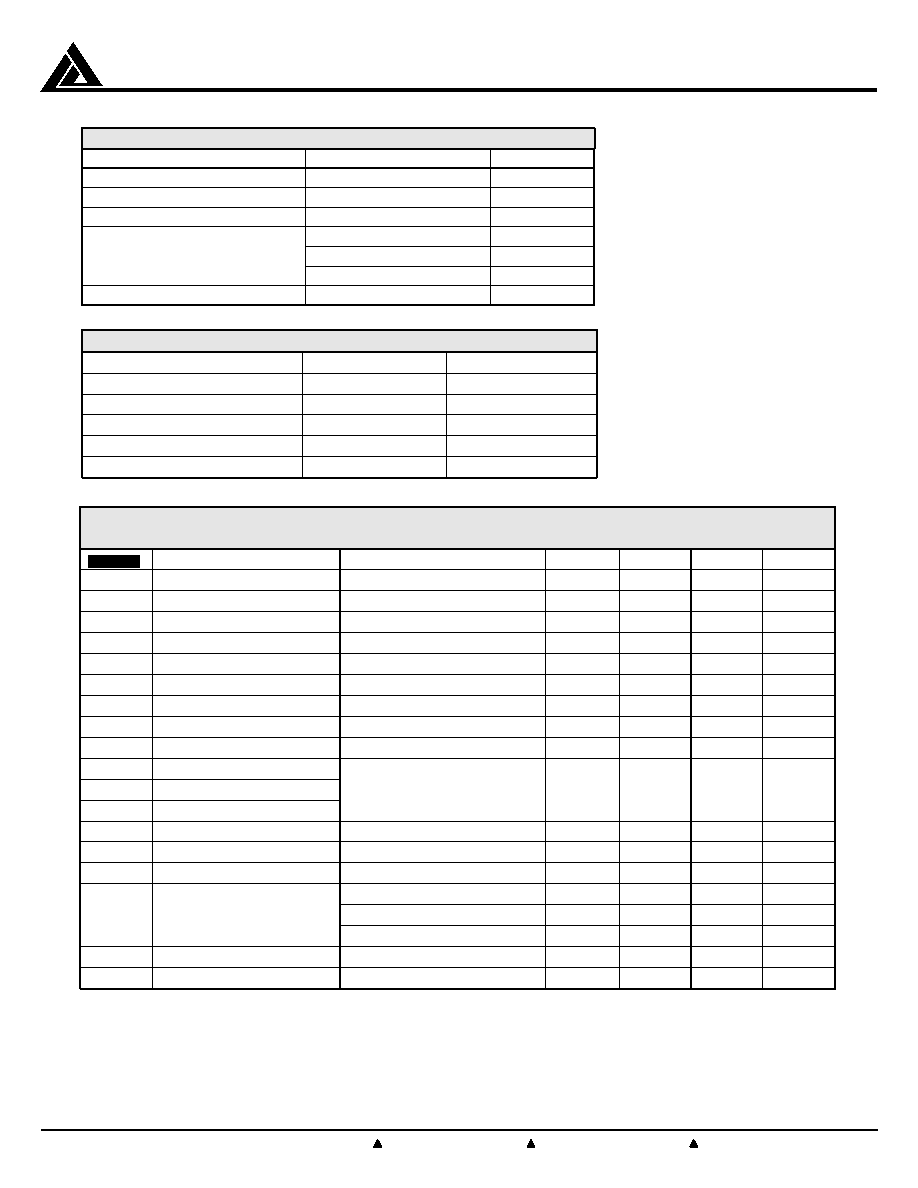
Typical Application Circuit
V
CC
V
CC
V
AUX
V
SBY
GND
GND
V
OUT
V
OUT
3.3V
400mA
CMPWR330
V
AUX
3.3V
10µF
+
+
1µF
V
SBY
GND
+
1µF
5V
5V
CALIFORNIA MICRO DEVICES
©2001 California Micro Devices Corp. All rights reserved. Smart ORTM is a trademark of California Micro Devices.
3/6/2001
215 Topaz Street, Milpitas, California 95035
Tel: (408) 263-3214 Fax: (408) 263-7846 www.calmicro.com
2
CMPWR330
ABSOLUTE MAXIMUM RATINGS
Parameter
Rating
Unit
ESD Protection (HBM)
2000
V
V
CC,
V
SBY
Input Voltage
6.0, GND 0.5 V
V
AUX
Input Voltage
4.0, GND 0.5 V
Temperature: Storage
40 to 150
°C
Operating Ambient
0 to 70
°C
Operating Junction
0 to 125
°C
Power Dissipation:
(Note 1)
Internally
Limited
W
OPERATING CONDITIONS
Parameter
Range
Unit
V
CC
, V
SBY
5 ± 0.25
V
V
AUX
3.3 ± 0.3
V
Temperature (Ambient)
0 to 70
°C
Load Current
0 to 400
mA
C
EXT
10 ± 20%
µF
ELECTRICAL OPERATING CHARACTERISTICS
(over operating conditions unless specified otherwise)
Parameter
Conditions
MIN
TYP
MAX
UNIT
V
OUT
Regulator Output Voltage
0mA < I
LOAD
< 400mA
3.135
3.30
3.465
V
I
LIM
Regulator
Current
Limit
500
mA
I
S/C
Short Circuit Current
V
CC/SBY
= 5V,
V
out
= 0V
150
mA
V
R LOAD
Load Regulation
V
CC
= 5V,
I
LOAD
= 5 to 400mA
20
mV
V
R LINE
Line
Regulation
V
CC
= 4.5V to 5.5V,
I
LOAD
= 5mA
2
mV
V
CCSEL
V
CC
Select Voltage
V
SBY
or V
AUX
present
4.40
4.60
V
V
CCDES
V
CC
Deselect Voltage
V
SBY
or V
AUX
present
4.00
4.20
V
V
HYST
Hysteresis
Voltage
(Note 2)
V
SBY
or V
AUX
present
0.20
V
R
SW
V
AUX
Switch Resistance
0.25
0.4
I
RCC
V
CC
Reverse Leakage
One supply input taken to
I
RSBY
V
SBY
Reverse Leakage
ground while the others remain
5 100 µA
I
RAUX
V
AUX
Reverse Leakage
at nominal voltage
I
CC
V
CC
Supply Current
V
CC
> V
CCSEL
,
I
LOAD
= 0mA
0.8
1.5
mA
I
SBY
V
SBY
Supply Current
V
CC
< V
CCDES
,
I
LOAD
= 0mA
0.8
1.5
mA
I
AUX
V
AUX
Supply Current
V
AUX
is selected, I
LOAD
= 0mA
0.2
0.30
mA
I
GND
Ground
Current
V
AUX
is selected, (v
CC/SBY
= 0V)
0.2 0.30 mA
V
CC/SBY
= 5V, I
LOAD
= 0mA
0.8
1.5
mA
V
CC/SBY
= 5V, I
LOAD
= 400mA
1.0 2.0 mA
T
DISABLE
Shutdown
Temperature
160
°C
T
HYST
Thermal
Hysteresis
20
°C
Note 1: At rated load, the power dissipation will be 0.68W (1.7V x 0.4A). Under these conditions, (in a 70°C ambient), the thermal
resistance from junction to ambient (
JA
) must not exceed 80°C/W. This is typically achieved with 2 square inches of copper printed
circuit board area connected to the GND pins for heat spreading, or equivalent.
Note 2: The disturbance on V
CC
during supply changeover should be kept below the hysteresis voltage to prevent any chatter. The source
resistance on the V
CC
supply should be kept to less than 0.3
to ensure precise switching.
CALIFORNIA MICRO DEVICES
3/6/2001
3
215 Topaz Street, Milpitas, California 95035
Tel: (408) 263-3214 Fax: (408) 263-7846 www.calmicro.com
CMPWR330
©2001 California Micro Devices Corp. All rights reserved. Smart ORTM is a trademark of California Micro Devices.
Interface Signals
V
CC
is a positive input supply for the voltage regulator.
Whenever this supply voltage exceeds the V
CCSEL
level
(4.4V), it will immediately be given priority and be used
to power the regulator output. If this supply voltage falls
below the V
CCDES
level (4.2V) it will immediately be
deselected and no longer provide power for the regula-
tor output. An internal hysteresis voltage of 0.2V is used
to prevent any chatter during selection and deselection
of V
CC
. The effective source impedance of V
CC
should be
kept below 0.3
to ensure changeover disturbances do
not exceed the hysteresis level.
If the connection to V
CC
is made within a few inches of
the main input filter, a bypass capacitor may not be
necessary. Otherwise a bypass filter capacitor in the
range of 1µF to 10µF will ensure adequate filtering.
V
SBY
is the standby input supply (5V), which is immedi-
ately used to power the regulator output whenever V
CC
is
below the deselect level (4.2V).
If the V
SBY
connection is made within a few inches of the
main input filter, a bypass capacitor may not be neces-
sary. Otherwise a bypass filter capacitor in the range of
1µF to 10µF will ensure adequate filtering.
V
AUX
is the auxiliary voltage power source. This supply is
selected only when V
CC
falls below 4.2V and the V
SBY
is
not present. Under these conditions an internal switch is
enabled and provides a very low impedance connection
directly between V
OUT
and V
AUX
.
V
OUT
is the output voltage. Power is provided from the
regulator or via the low impedance auxiliary switch. This
output requires a capacitance of 10µF to ensure regula-
tor stability and minimize the peak output disturbance
during power supply changeover.
GND provides the reference for all voltages.
INTERFACE SIGNALS
Pin
Symbol
Description
1
V
SYB
Standby supply voltage (5V) input for regulator whenever V
CC
falls below 4.2V.
2
V
CC
Primary supply voltage (5V) input for regulator
3
V
OUT
Regulator voltage output (3.3V) regulator when either V
CC
or V
SYB
is present
4
V
AUX
Auxiliary supply voltage (3.3V) input for low impedance switch
5 - 8
GND
Reference for all voltages
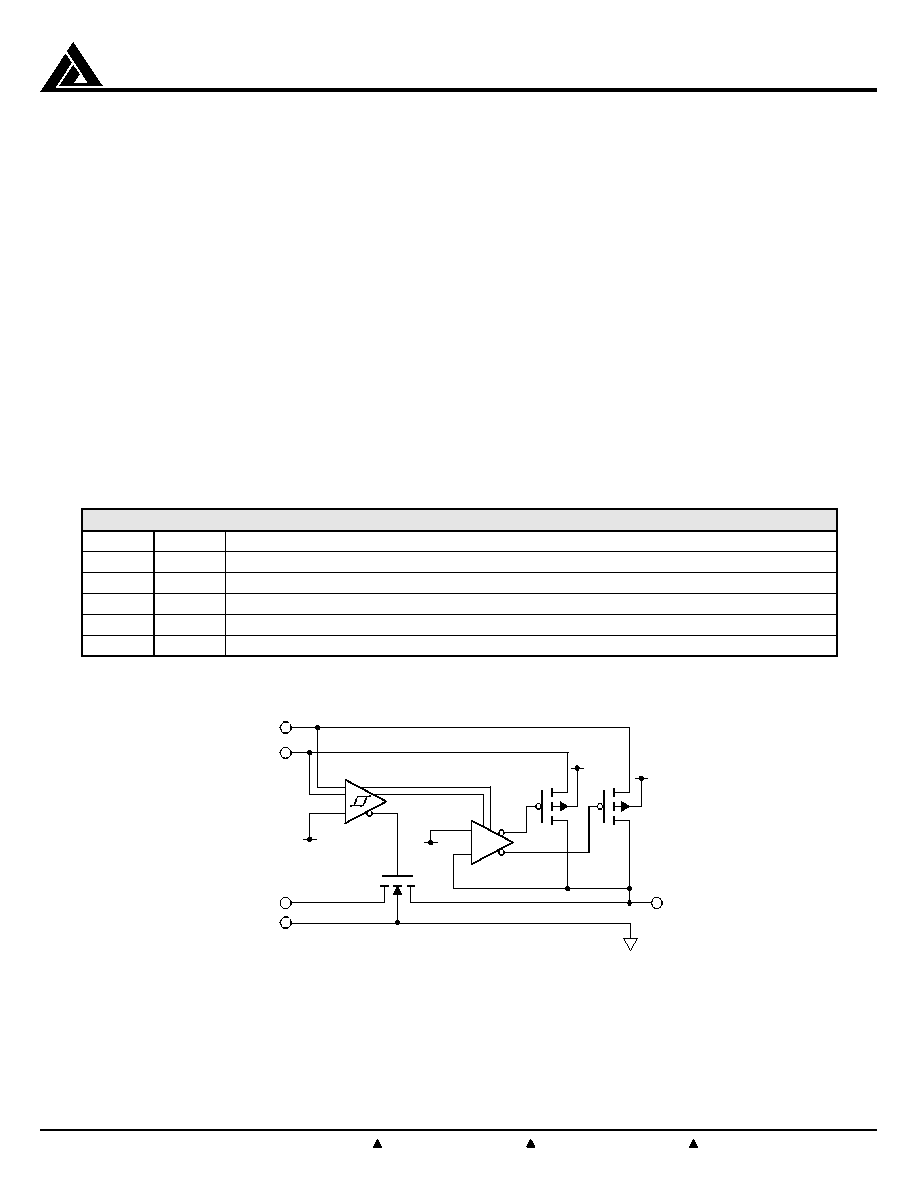
Simplified Electrical Schematic
V
OUT
3.3V
400mA
V
REF
3.3V
+
5V
CC
+
+
V
DESELECT
4.2V
CONTROLLER
REGULATOR AMP
ENABLE
SELECT (V
CC
/V
SBY
)
5V
SBY
3.3V
AUX
GND
GND
V
SBY
V
CC
A
UX
S
W
0.25
A
UX
S
W
CALIFORNIA MICRO DEVICES
©2001 California Micro Devices Corp. All rights reserved. Smart ORTM is a trademark of California Micro Devices.
3/6/2001
215 Topaz Street, Milpitas, California 95035
Tel: (408) 263-3214 Fax: (408) 263-7846 www.calmicro.com
4
CMPWR330
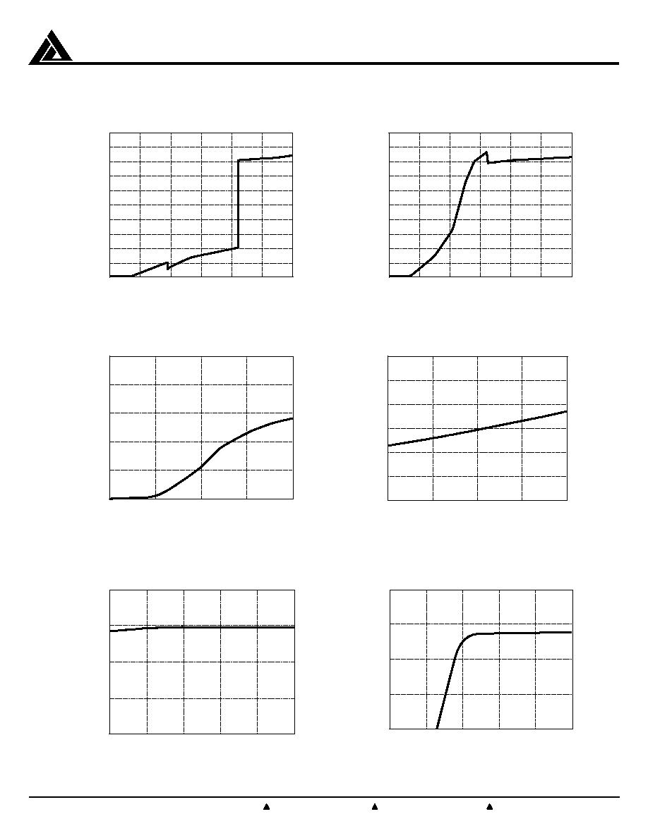
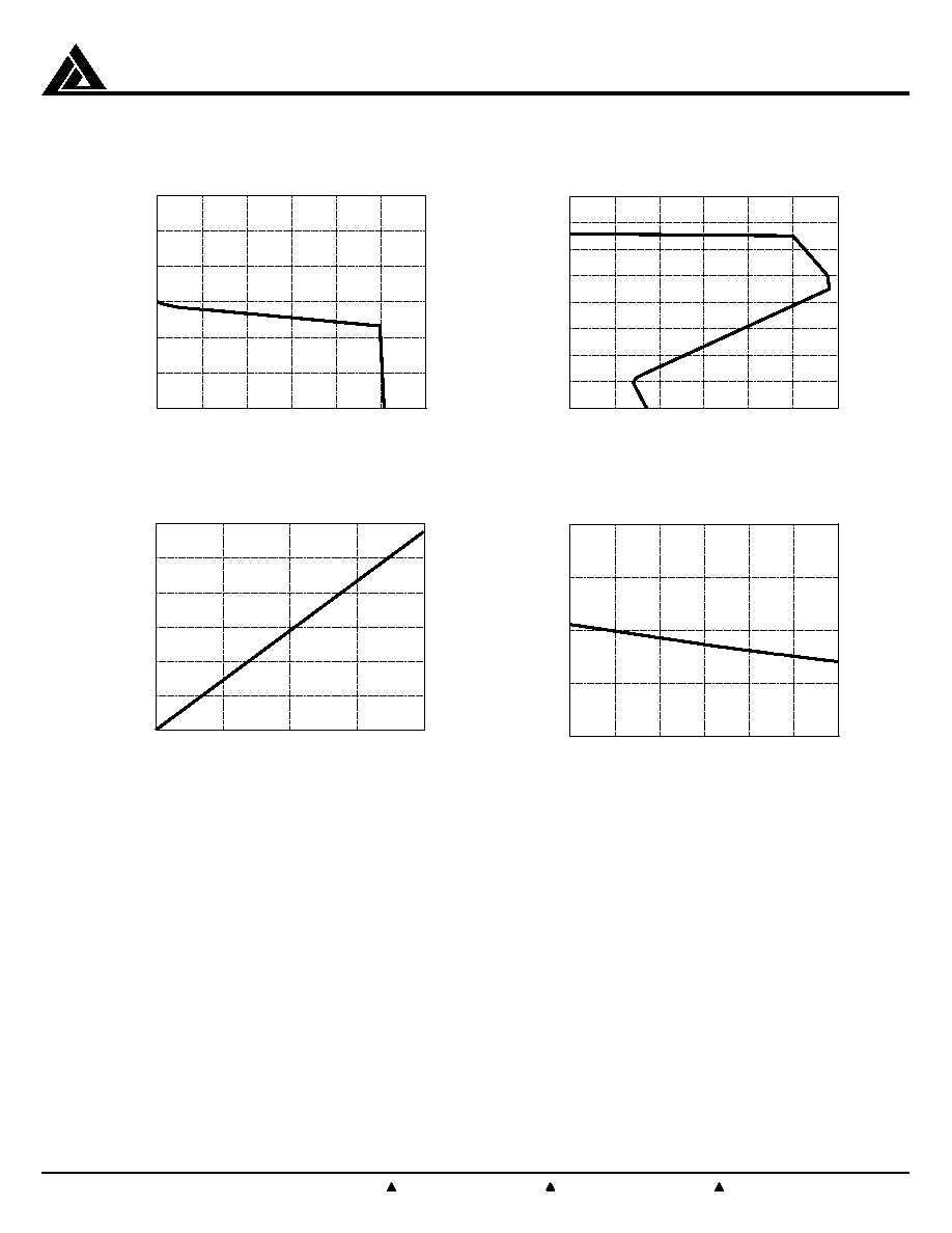
Figure 1. V
CC
Supply Current vs Voltage
Figure 2. V
SBY
Supply Current vs Voltage
Figure 3. V
AUX
Supply Current vs Voltage
Figure 4. Ground Current vs Output Load
Figure 5. Line Regulation (5mA Load)
Figure 6. Line Regulation (400mA Load)
0
1
2
3
4
5
6
V
CC
Input Voltage (V)
0.0
0.1
0.2
0.3
0.4
0.5
0.6
0.7
0.8
0.9
1.0
Suppl
y
Current (mA)
0
1
2
3
4
5
6
V
SBY
Input Voltage (V)
0.0
0.1
0.2
0.3
0.4
0.5
0.6
0.7
0.8
0.9
1.0
Suppl
y
Current (mA)
3.5
4
4.5
5
5.5
6
Line Voltage (V)
3.0
3.1
3.2
3.3
3.4
Regulator Output
V
olta
g
e
(V)
3.5
4
4.5
5
5.5
6
Line Voltage (V)
3.0
3.1
3.2
3.3
3.4
Regulator Output
V
o
lta
g
e
(V)
Typical DC Characteristics (nominal conditions unless specified otherwise)
0
100
200
300
400
Load Current (mA)
0.6
0.7
0.8
0.9
1.0
1.1
1.2
Gr
ound Current (mA)
0
1
2
3
4
V
AUX
Input Voltage (V)
0.0
0.1
0.2
0.3
0.4
0.5
Suppl
y Current (mA)
CALIFORNIA MICRO DEVICES
3/6/2001
5
215 Topaz Street, Milpitas, California 95035
Tel: (408) 263-3214 Fax: (408) 263-7846 www.calmicro.com
CMPWR330
©2001 California Micro Devices Corp. All rights reserved. Smart ORTM is a trademark of California Micro Devices.
Typical DC Characteristics
Figure 7. Load Regulation (5V Supply)
Figure 8. Foldback Current Limit Protection
Figure 9. Regulator Dropout Characteristics
Figure 10. Switch Resistance vs V
AUX
Supply
0
100
200
300
400
500
600
Load Current (mA)
3.15
3.20
3.25
3.30
3.35
3.40
3.45
Regulator Output
V
olta
g
e
(V)
0
100
200
300
400
Load Current (mA)
0.0
0.2
0.4
0.6
0.8
1.0
1.2
Dr
opout V
olta
g
e
(V)
3.0
3.1
3.2
3.3
3.4
3.5
3.6
V
AUX
INPUT VOLTAGE (V)
0.20
0.25
0.30
0.35
0.40
ON Resisitance (
)
0
100
200
300
400
500
600
Output Current (mA)
0.0
0.5
1.0
1.5
2.0
2.5
3.0
3.5
4.0
Regulator Output
V
olta
g
e
(V)