 | ÐлекÑÑоннÑй компоненÑ: CPCI102BR | СкаÑаÑÑ:  PDF PDF  ZIP ZIP |
Äîêóìåíòàöèÿ è îïèñàíèÿ www.docs.chipfind.ru
©
2005 California Micro Devices Corp. All rights reserved.
02/28/05
430 N. McCarthy Blvd., Milpitas, CA 95035-5112
Tel: 408.263.3214
Fax: 408.263.7846
www.calmicro.com
1
CMCPCI102B
CompactPCI
®
Backplane Interface
Features
·
CompactPCI® standards compliant
·
Allows CompactPCI System Cards to be
used in any Slot
·
Provides termination for up to ten channels
·
Provides a series switch in each channel
·
Supports hot-swap capability
·
Very low capacitance load on each line
·
Industrial temperature range
·
28-pin TSSOP package
·
Lead-free version available
Applications
·
Redundant System CompactPCI® cards
·
Hot-swap CompactPCI cards
·
Industrial PCs
·
Telecom/Datacom equipment
·
Instrumentation
·
Computer Telephony
·
Real-time machine control
Product Description
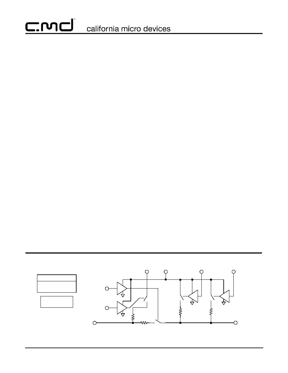
The CMCPCI102BT/BR is a 10-channel backplane
interface/termination IC specifically designed for Com-
pactPCI redundant system-slot cards. The
CMCPCI102BT/BR allows CompactPCI boards to
interface to the backplane and provides the versatility
to use system cards in any slot (system or peripheral).
Per the CompactPCI specification, the CMCPCI102BT/
BR provides a 10
termination resistor for each chan-
nel to terminate the transmission line stub on the
board. An integral series switch and associated control
signal (SW_EN) permits connection/disconnection of
the channel, so that the device side of the circuit may
be isolated from the backplane side.
The CompactPCI standard requires system boards to
be hot-swappable. To accommodate this requirement,
the CMCPCI102BT/BR features a switched 10k
resis-
tor connected to the 1V Precharge Supply Voltage. If
the precharge enable pin (P_EN) is asserted, then the
10k
pull-up resistors are connected to precharge the
circuits.
In addition, a system board requirement mandates
either a 1.0k
pull-up resistor or a 2.7k resistor con-
nected to VIO. CompactPCI slot cards must work in
either 3.3V or 5V systems, hence the need for both
2.7k
and 1k resistors. If the 3_EN pin is logic high,
the 2.7k
resistor is used as the pull-up. If the 5_EN pin
is logic high, the 1k
resistor is used.
The CMCPCI102BT/BR integrates all these functions in
a low-profile 28-pin TSSOP package and is available
with optional lead-free finishing.
Simplified Electrical Schematic
*One of 10 parallel
channels is shown.
1V
5_EN
3_EN
VIO
B1-B10*
A1-A10*
CompactPCI Device Side
Backplane Side
P_EN
SW_EN
For all Enable signals:
Logic 0 = switch open
Logic 1 = switch closed
R
S
10
R
PU1
10k
SW
PU1
SW
PU2
SW
PU3
R
PU2
2.7k
R
PU3
1k
SW
S
©
2005 California Micro Devices Corp. All rights reserved.
2
430 N. McCarthy Blvd., Milpitas, CA 95035-5112
Tel: 408.263.3214
Fax: 408.263.7846
www.calmicro.com
02/28/05
CMCPCI102B
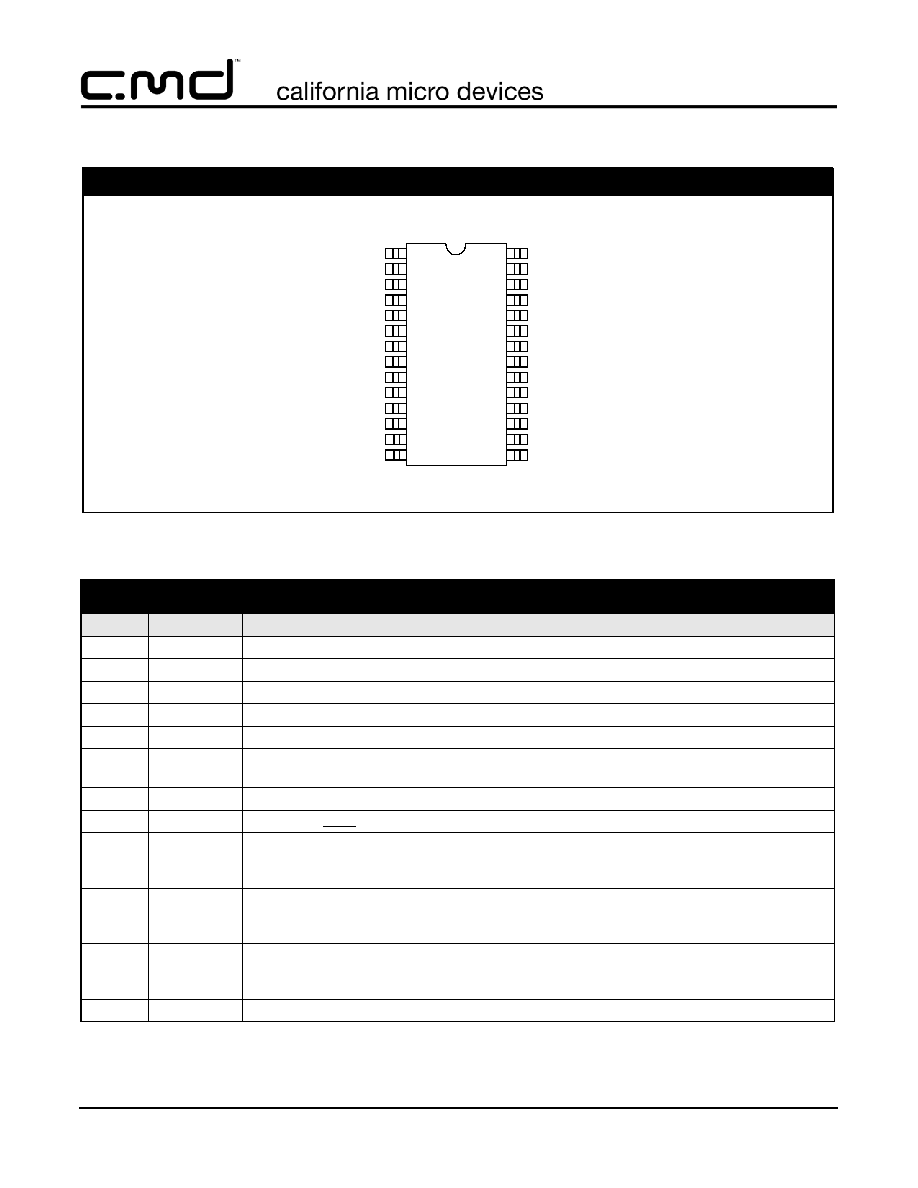
PIN DESCRIPTIONS
PIN(S)
NAME
DESCRIPTION
1-5
A1 - A5
The backplane-side input signals for channels 1 through 5, respectively.
10-14
A6 - A10
The backplane-side input signals for channels 6 through 10, respectively.
24-28
B1 - B5
The device-side connection for channels 1 through 5, respectively.
15-19
B6 - B10
The device-side connection for channels 6 through 10, respectively.
6
1V
A precharge supply voltage input for all channels. This voltage can be less than or equal to VIO.
7
P_EN
The precharge enable input which controls the precharge pull-up resistors. When this active high
control signal is set to '1', the precharge of all channels is enabled.
8
GND
The ground voltage reference for the CMCPCI102BT/BR.
9
CAP
A capacitor must be placed from this pin to GND. The recommended value is 0.01
µF,16V.
20
SW_EN
The series switch enable input. When this active high control signal is set to '1', the series switch
between the channel's backplane-side terminal and device-side terminal is closed. When this sig-
nal is cleared to '0', the switch is open.
21
3_EN
The enable signal for the device-side channel pull-up mechanism when 3.3V is the supply volt-
age. When this active high control signal is set to '1', the 2.7k
pull-up resistor which pulls up the
channel to the supply rail is engaged. Otherwise, this pin should be set to '0'.
22
5_EN
The enable signal for the device-side channel pull-up mechanism when 5V is the supply voltage.
When this active high control signal is set to '1', the 1k
pull-up resistor which pulls up the channel
to the supply rail is engaged. Otherwise, this pin should be set to '0'.
23
VIO
The positive supply voltage for the CMCPCI102BT/BR. Either 3.3V or 5V may be used.
28-pin TSSOP
1
2
3
4
5
6
7
8
20
19
18
17
21
22
9
10
24
23
25
26
11
12
27
28
A5
1V
P_EN
GND
CAP
A6
A7
A8
A1
A2
A3
A4
B2
B3
B4
B5
VIO
5_EN
3_EN
SW_EN
B6
B7
B8
B1
13
14
16
15
B9
B10
A9
A10
PACKAGE / PINOUT DIAGRAM
Note: This drawing is not to scale.
Top View
©
2005 California Micro Devices Corp. All rights reserved.
02/28/05
430 N. McCarthy Blvd., Milpitas, CA 95035-5112
Tel: 408.263.3214
Fax: 408.263.7846
www.calmicro.com
3
CMCPCI102B
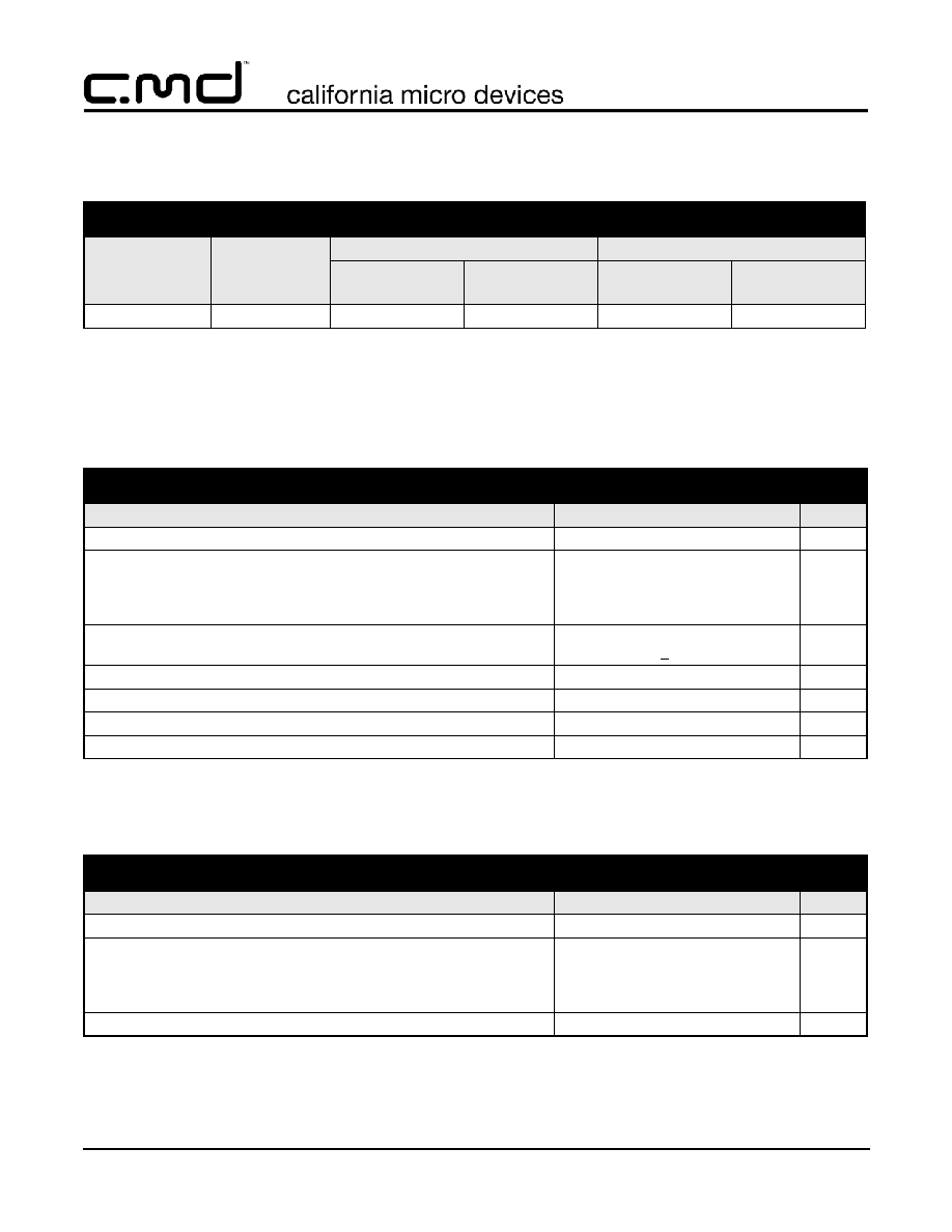
Ordering Information
Note 1: Parts are shipped in Tape & Reel form unless otherwise specified.
Specifications
Note 1: ESD is applied to input / output pins with respect to GND, one at a time; unused pins are left open.
Note 2: This parameter guaranteed by design.
PART NUMBERING INFORMATION
Pins
Package
Standard Finish
Lead-free Finish
Ordering Part
Number
1
Part Marking
Ordering Part
Number
1
Part Marking
28
TSSOP
CMCPCI102BT
CPCI102B
CMCPCI102BR
CPCI102BR
ABSOLUTE MAXIMUM RATINGS
PARAMETER
RATING
UNITS
VIO (supply voltage)
-0.5 to +6
V
Pin Voltages
1V, P_EN, 3_EN, 5_EN, SW_EN
A1-A10
B1-B10
-0.5 to (VIO+0.5)
-0.5 to (VIO+0.5)
-0.5 to (VIO+0.5)
V
V
V
ESD Withstand Voltage
Human Body Model, MIL-STD-883D, Method 3015 (Notes 1, 2)
+2000
V
Storage Temperature Range
-65 to +150
°C
Operating Temperature Range (Ambient)
-40 to +85
°C
DC Power per Resistor
62
mW
Package Power Rating
1
W
STANDARD OPERATING CONDITIONS
PARAMETER
RATING
UNITS
VIO (supply voltage)
3 to 5.5
V
Pin Voltages
P_EN, 3_EN, 5_EN, SW_EN, 1V
A1-A10
B1-B10
0 to VIO
0 to VIO
0 to VIO
V
V
V
Ambient Operating Temperature Range
-40 to +85
°C
©
2005 California Micro Devices Corp. All rights reserved.
4
430 N. McCarthy Blvd., Milpitas, CA 95035-5112
Tel: 408.263.3214
Fax: 408.263.7846
www.calmicro.com
02/28/05
CMCPCI102B
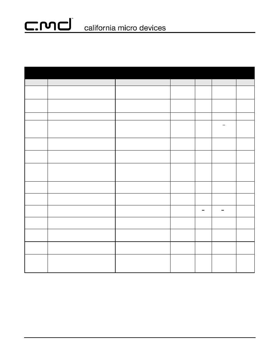
Specifications (Cont'd)
Note 1: Operating Characteristics are over Standard Operating Conditions unless otherwise specified.
Note 2: This parameter is guaranteed by design; it is not tested 100%.
ELECTRICAL OPERATING CHARACTERISTICS
(NOTE 1)
SYMBOL PARAMETER
CONDITIONS
MIN
TYP
MAX
UNITS
R
S1
Series Resistance through R
S
A to B; switch SW
S
closed;
T
A
=25°C
5
10
15
R
S2
Series Resistance through R
S
A to B; switch SW
S
open;
T
A
=25°C
1
M
R
PU1
Resistance of R
PU1
pull-up
T
A
=25°C
9.5
18
k
TOL
RPU2
TOL
RPU3
Resistance Tolerance
(R
PU2
and R
PU3
)
T
A
=25°C
+5
%
TCR
PU
Temperature Coefficient of
Resistance (R
PU1
, R
PU2
, R
PU3
)
-100
ppm/°C
C
1
Capacitance on backplane side
(A side) of series resistor R
S
Measured @ 66MHz,
0VDC, SW_EN=0V; Note 2
1.9
pF
C
2
Capacitance on device side (B
side) of series resistor R
S
and
series switch SW
S
Measured @ 66MHz,
0VDC, VIO=5V, 5_EN=5V
SW_EN=0V; Note 2
4.2
pF
V
IL
Logic Low Input Voltage to P_EN,
3_EN, 5_EN, SW_EN
-0.5
[VIO] x 0.3
V
V
IH
Logic High Input Voltage to P_EN,
3_EN, 5_EN, SW_EN
[VIO] x 0.7
[VIO] + 0.5
V
I
LEAK
Leakage Current into P_EN, 3_EN,
5_EN, SW_EN
GND < V < VIO
+1
+10
µA
I
GND
Supply Current for internal circuits
(measured at GND pin)
0.25
1
m
A
t
PLH
Switch SW
S
closure delay from the
low-to-high transition of SW_EN
Note 2, 'CAP' pin capaci-
tor=0.01
µF
14
ms
t
PHL
Switch SW
S
delay from the high-to-
low transition of SW_EN
Note 2, 'CAP' pin capaci-
tor=0.01
µF
12
µs
t
PPU
Propagation delay for pull-up
switches SW
PU1
,
SW
PU2
, and
SW
PU3
, all transitions
Note 2
10
ns
©
2005 California Micro Devices Corp. All rights reserved.
02/28/05
430 N. McCarthy Blvd., Milpitas, CA 95035-5112
Tel: 408.263.3214
Fax: 408.263.7846
www.calmicro.com
5
CMCPCI102B
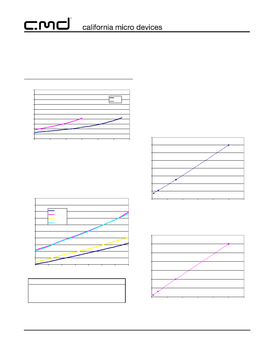
Performance Information
Resistance Variation with Input Voltage
The series resistance R
S
varies with input voltage and
supply voltage, as shown in
Figure 1
.
Figure 1. Resistance Variation vs. Input Voltage
Resistance Variation with Temperature
The series resistance R
S
also varies with temperature,
as shown in
Figure 2
.
Figure 2. Resistance Variation vs. Temperature
CAP Pin Capacitance
Some external capacitance is necessary to prevent the
voltage on the CAP pin from falling during sustained
data transfers through the device. This ensures that
the logic 1 level does not degrade.
The time required to open and close the series switch,
SWs, varies according to how much capacitance is
present on the CAP pin.
The minimum usable value is 200pF, placed close to
the pins. A 0.01uF, 16V capacitor is recommended.
See
Figure 3
and
Figure 4
for variation of switch on/off
times vs. capacitance.
Figure 3. Switch ON Time vs. CAP Capacitor Value
Figure 4. Switch OFF Time vs. CAP Capacitor Value
Variation of 10R Resistor with I/O Voltage, T=25'C
5
6
7
8
9
10
11
12
13
14
15
0
1
2
3
4
5
6
I/O Voltage [ V ]
R
e
si
st
an
ce
[
]
Vcc5.5
Vcc3.0
CONDITIONS:
Curve V
CC
3V
IN
0:
Curve V
CC
3V
IN
3:
Curve V
CC
5V
IN
0:
Curve V
CC
5V
IN
5:
V
IO
= 3.0V
V
IO
= 3.0V
V
IO
= 5.5V
V
IO
= 5.5V
channel voltage = 0.0V
channel voltage = 3.0V
channel voltage = 0.0V
channel voltage = 5.5V
Temperature Variation of 10R Resistor
5
6
7
8
9
10
11
12
13
14
15
-40
-20
0
20
40
60
80
100
Temperature [
o
C ]
R
esi
st
an
ce
[
]
V
CC
5V
IN
0
V
CC
5V
IN
5
V
CC
3V
IN
0
V
CC
3V
IN
3
Switch ON Time vs. CAP Capacitor Value
0
2
4
6
8
10
12
14
16
0
2000
4000
6000
8000
10000
12000
Capacitor Value on CAP Pin [pF]
S
W
s
C
l
o
s
i
n
g
Ti
m
e
[mS]
Switch OFF Time vs. CAP Capacitor Value
0
2
4
6
8
10
12
14
0
2000
4000
6000
8000
10000
12000
Capacitor Value on CAP Pin [pF]
S
W
s
O
pe
ni
ng
T
i
m
e
[
µ
S]
Document Outline