Äîêóìåíòàöèÿ è îïèñàíèÿ www.docs.chipfind.ru
© 2003 California Micro Devices Corp. All rights reserved.
10/10/03
430 N. McCarthy Blvd., Milpitas, CA 95035-5112
L Tel: 408.263.3214
L Fax: 408.263.7846 L www.calmicro.com
1
CSPEMI307A
4-Channel ESD/EMI Filter Array plus
4-Channel ESD Array for USB
Features
·
Four channels of combined EMI/RFI filtering +
ESD protection
·
Four additional channels of ESD-only protection
·
EMI/ESD channels provide greater than 32dB
attenuation at 1GHz
·
+
15kV ESD protection on all channels
(IEC 61000-4-2 Level 4, contact discharge)
·
+
30kV ESD protection on all channels (HBM)
·
Chip Scale Package features extremely low
lead inductance for optimum filter and ESD
performance
·
15-bump, 2.960mm X 1.330mm footprint
Chip Scale Package (CSP)
·
Lead-free version available
Applications
·
EMI filtering and ESD protection for both data and
I/O ports
·
Outer 4 channels provide ESD protection for
USB lines and other I/O port applications
·
Wireless Handsets
·
Handheld PCs / PDAs
·
MP3 Players
·
Notebooks
·
Desktop PCs
Product Description
The CSPEMI307A is a multichannel EMI/ESD array
offering a combination of four low-pass filter + ESD
channels to reduce EMI/RFI emissions on a data port
and four dedicated ESD-only channels intended specif-
ically for ESD protection on a USB port. Each EMI/RFI
channel integrates a high quality pi-style filter (C-R-C)
which provides greater than 30dB attenuation in the
800-2700 MHz range. These pi-style filters support
bidirectional filtering, controlling EMI both to and from a
data port connector.
The CSPEMI307A provides a high-level of ESD protec-
tion on all eight channels for sensitive electronic com-
ponents that may be subjected to electrostatic
discharge (ESD). The input pins are designed and
characterized to safely dissipate ESD strikes of 15kV,
exceeding the maximum requirement of the IEC
61000-4-2 international standard. Using the MIL-STD-
883 (Method 3015) specification for Human Body
Model (HBM) ESD, the device provides protection for
contact discharges to greater than 30kV.
The CSPEMI307A is particularly well suited for porta-
ble electronics (e.g., cellular telephones, PDAs, note-
book computers) because of its small package footprint
and low weight. The CSPEMI307A is available in a
space-saving, low-profile Chip Scale Package with
optional lead-free finishing.
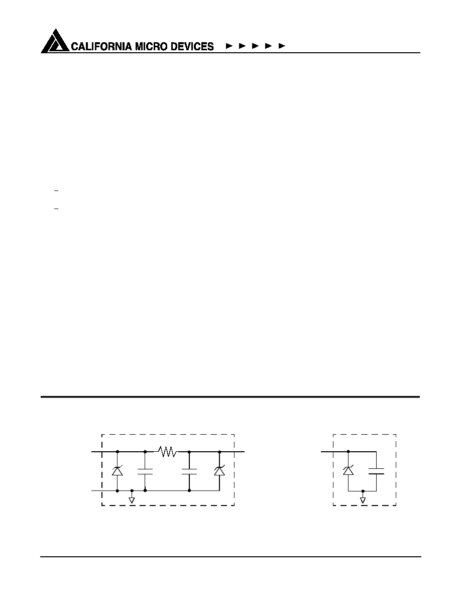
Electrical Schematic
100
30pF
30pF
FILTER+ESDn*
GND
FILTER+ESDn*
1 of 4 EMI/RFI + ESD Channels.
(Pins B1-B3)
30pF
ESDn*
1 of 4 ESD-only Channels
* See Package/Pinout Diagram for expanded pin information
© 2003 California Micro Devices Corp. All rights reserved.
2
430 N. McCarthy Blvd., Milpitas, CA 95035-5112
L Tel: 408.263.3214
L Fax: 408.263.7846 L www.calmicro.com
10/10/03
CSPEMI307A
Ordering Information
Note 1: Parts are shipped in Tape & Reel form unless otherwise specified.
Note 2: Lead-free devices are specified by using a "
+
" character for the top side orientation mark.
PIN DESCRIPTIONS
PIN(s)
NAME
DESCRIPTION
A1
ESD_1
ESD Channel 1
A2
FILTER+ESD_1
Filter + ESD Channel 1
A3
FILTER+ESD_2
Filter + ESD Channel 2
A4
FILTER+ESD_3
Filter + ESD Channel 3
A5
FILTER+ESD_4
Filter + ESD Channel 4
A6
ESD_2
ESD Channel 2
B1-B3
GND
Device Ground
C1
ESD_3
ESD Channel 3
C2
FILTER+ESD_1
Filter + ESD Channel 1
C3
FILTER+ESD_2
Filter + ESD Channel 2
C4
FILTER+ESD_3
Filter + ESD Channel 3
C5
FILTER+ESD_4
Filter + ESD Channel 4
C6
ESD_4
ESD Channel 4
FILTER/ESD_4
ESD_2
GND
FILTER/ESD_4
ESD_4
A6
A5
Orientation
Marking
B3
C6
C5
FILTER/ESD_2
FILTER/ESD_3
GND
FILTER/ESD_2
FILTER/ESD_3
A4
A3
B2
C4
C3
ESD_1
FILTER/ESD_1
GND
ESD_3
FILTER/ESD_1
A2
A1
B1
C2
C1
A1
307A
4
3
2
6
5
1
C
B
A
Orientation
Marking
(see note 2)
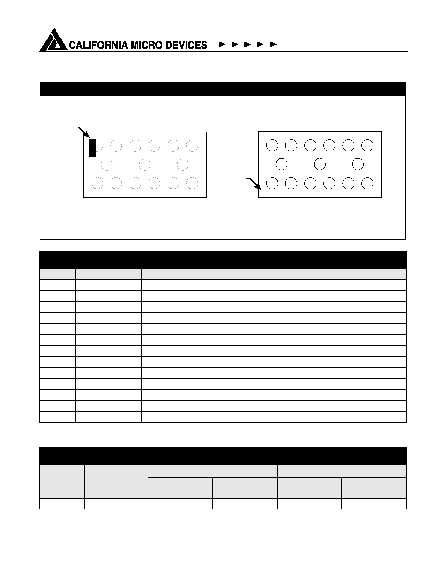
PACKAGE / PINOUT DIAGRAMS
Notes:.
BOTTOM VIEW
CSP Package
(Bumps Up View)
TOP VIEW
(Bumps Down View)
CSPEMI307A
1) These drawings are not to scale.
2) Lead-free devices are specified by using a "+" character for the top side orientation mark.
PART NUMBERING INFORMATION
Bumps
Package
Standard Finish
Lead-free Finish
2
Ordering Part
Number
1
Part Marking
Ordering Part
Number
1
Part Marking
15
CSP
CSPEMI307A
307A
CSPEMI307AG
307A
© 2003 California Micro Devices Corp. All rights reserved.
10/10/03
430 N. McCarthy Blvd., Milpitas, CA 95035-5112
L Tel: 408.263.3214
L Fax: 408.263.7846
L www.calmicro.com
3
CSPEMI307A
Specifications
Note 1: T
A
=25
°
C unless otherwise specified.
Note 2: ESD applied to input and output pins with respect to GND, one at a time.
Note 3: Clamping voltage is measured at the opposite side of the EMI filter to the ESD pin. For example, if ESD is applied to Pin A2,
then clamping voltage is measured at Pin C2.
Note 4: Unused pins are left open
Note 5: These parameters are guaranteed by design and characterization.
ABSOLUTE MAXIMUM RATINGS
PARAMETER
RATING
UNITS
Storage Temperature Range
-65 to +150
°C
DC Power per Resistor
100
mW
DC Package Power Rating
600
mW
STANDARD OPERATING CONDITIONS
PARAMETER
RATING
UNITS
Operating Temperature Range
-40 to +85
°C
ELECTRICAL OPERATING CHARACTERISTICS
1
SYMBOL
PARAMETER
CONDITIONS
MIN
TYP
MAX
UNITS
R
Resistance
80
100
120
C
Capacitance
At 2.5V DC
24
30
36
pF
TCR
Temperature Coefficient of Resistance
1200
ppm/°C
TCC
Temperature Coefficient of Capacitance
At 2.5V DC
-300
ppm/°C
V
DIODE
Diode Voltage (reverse bias)
I
DIODE
=10
µA
5.5
V
I
LEAK
Diode Leakage Current (reverse bias)
V
DIODE
=3.3V
100
nA
V
SIG
Signal Voltage
Positive Clamp
Negative Clamp
I
LOAD
= 10mA
5.6
-0.4
6.8
-0.8
9.0
-1.5
V
V
V
ESD
In-system ESD Withstand Voltage
a) Human Body Model, MIL-STD-883,
Method 3015
b) Contact Discharge per IEC 61000-4-2
Level 4
Notes 2,4 and 5
±30
±15
kV
kV
V
CL
Clamping Voltage during ESD Discharge
MIL-STD-883 (Method 3015), 8kV
Positive Transients
Negative Transients
Notes 2,3,4 and 5
+10
- 5
V
V
f
C
Cut-off frequency
Z
SOURCE
= 50
, Z
LOAD
= 50
R = 100
, C = 30pF
64
MHz
© 2003 California Micro Devices Corp. All rights reserved.
4
430 N. McCarthy Blvd., Milpitas, CA 95035-5112
L Tel: 408.263.3214
L Fax: 408.263.7846 L www.calmicro.com
10/10/03
CSPEMI307A
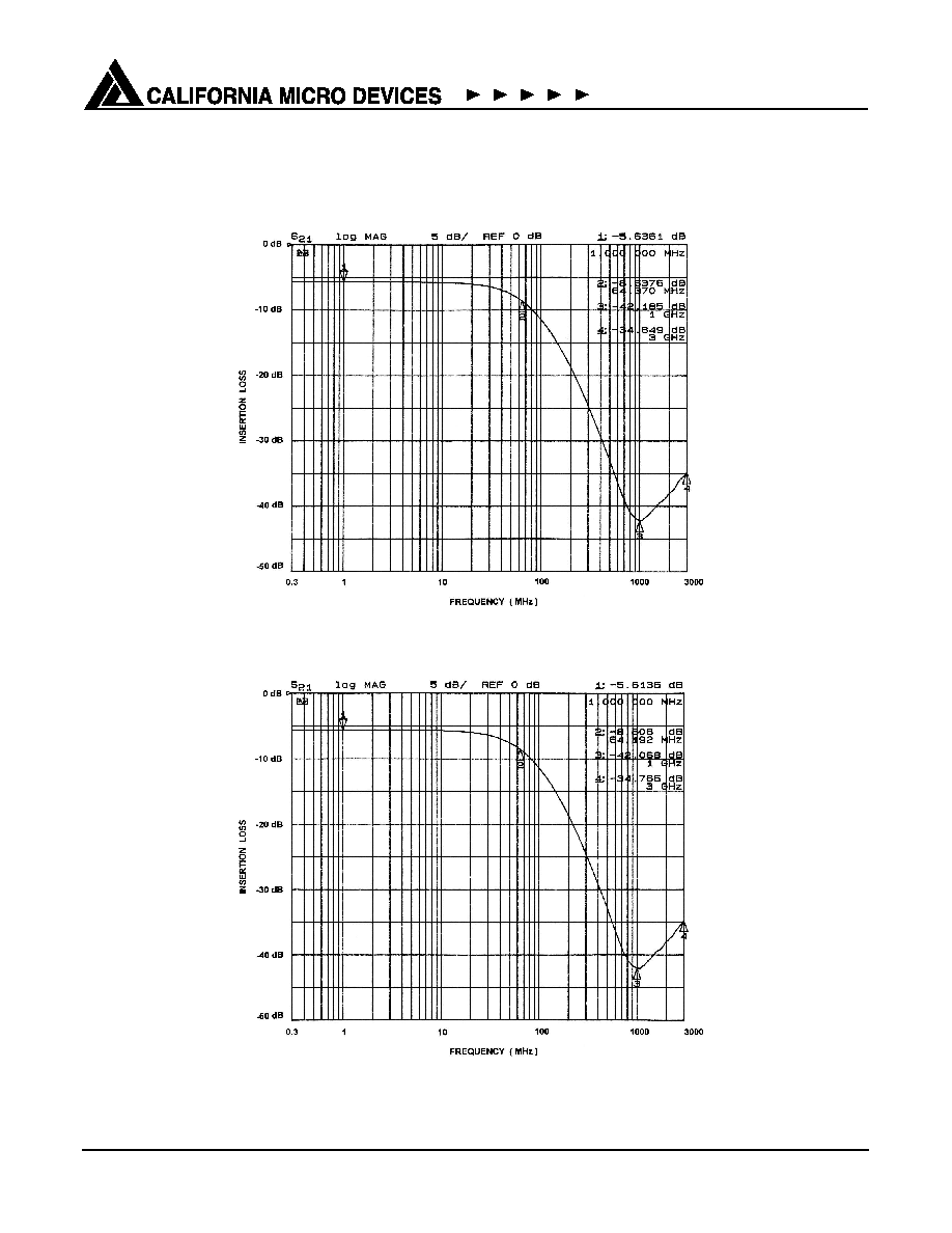
Performance Information
Typical Filter Performance (T
A
=25°C, DC Bias=0V, 50 Ohm Environment)
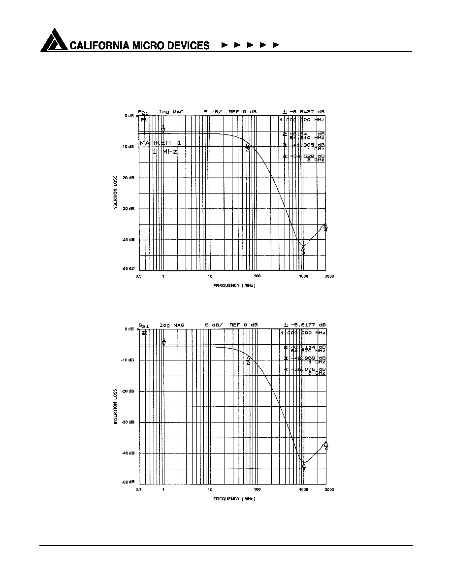
Figure 1. Insertion Loss VS. Frequency (A2-C2 to GND B2)
Figure 2. Insertion Loss VS. Frequency (A3-C3 to GND B2)
© 2003 California Micro Devices Corp. All rights reserved.
10/10/03
430 N. McCarthy Blvd., Milpitas, CA 95035-5112
L Tel: 408.263.3214
L Fax: 408.263.7846
L www.calmicro.com
5
CSPEMI307A
Performance Information
Typical Filter Performance (T
A
=25°C, DC Bias=0V, 50 Ohm Environment)
Figure 3. Insertion Loss VS. Frequency (A4-C4 to GND B2)
Figure 4. Insertion Loss VS. Frequency (A5-C5 to GND B2)
Document Outline