Äîêóìåíòàöèÿ è îïèñàíèÿ www.docs.chipfind.ru
© 2005 California Micro Devices Corp. All rights reserved.
09/28/05
490 N. McCarthy Blvd., Milpitas, CA 95035-5112
Tel: 408.263.3214
Fax: 408.263.7846
www.cmd.com
1
CSPEMI400
SIM Card EMI Filter Array with ESD Protection
Features
·
Three channels of EMI filtering, each with ESD
protection
·
Two additional channels of ESD-only protection
·
±10kV ESD protection (IEC 61000-4-2, contact
discharge)
·
±25kV ESD protection (HBM)
·
Greater than 30dB of attenuation at 1GHz
·
10-bump, 1.960mm x 1.330mm footprint Chip
Scale Package (CSP)
·
Lead-free version available
Applications
·
SIM Card slot in mobile handsets
·
I/O port protection for mobile handsets, notebook
computers, PDAs, etc.
·
EMI filtering for data ports in cell phones, PDAs or
notebook computers
Product Description
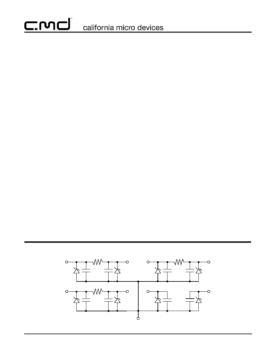
CAMD's CSPEMI400 is an EMI filter array with ESD
protection, which integrates three pi filters (C-R-C) and
two additional channels of ESD protection. The
CSPEMI400 has component values of 20pF-47
-
20pF, and 20pF-100
-20pF. The parts include ava-
lanche-type ESD diodes on every pin, which provide a
very high level of protection for sensitive electronic
components that may be subjected to electrostatic dis-
charge (ESD). The ESD diodes connected to the filter
ports safely dissipate ESD strikes of ±10kV, exceeding
the maximum requirement of the IEC 61000-4-2 inter-
national standard. Using the MIL-STD-883 (Method
3015) specification for Human Body Model (HBM)
ESD, the pins are protected for contact discharges at
greater than ±25kV.
The ESD diodes on pins A4 and C4 ports are designed
and characterized to safely dissipate ESD strikes of
±10kV, well beyond the maximum requirement of the
IEC 61000-4-2 international standard.
This device is particularly well suited for portable elec-
tronics (e.g. mobile handsets, PDAs, notebook com-
puters) because of its small package format and easy-
to-use pin assignments. In particular, the CSPEMI400
is ideal for EMI filtering and protecting data lines from
ESD for the SIM card slot in mobile handsets.
The CSPEMI400 is available in a space-saving, low-
profile Chip Scale Package with optional lead-free fin-
ishing.
Electrical Schematic
R
1
C
C
C1
B2,B4
GND
A1
R
2
C
C
C2
A2
C
C
C4
A4
R
1
C
C
C3
A3
R
1
=100
R
2
=47
© 2005 California Micro Devices Corp. All rights reserved.
2
490 N. McCarthy Blvd., Milpitas, CA 95035-5112
Tel: 408.263.3214
Fax: 408.263.7846
www.cmd.com
09/28/05
CSPEMI400
Ordering Information
Note 1: Parts are shipped in Tape & Reel form unless otherwise specified.
Note 2: Lead-free devices are specified by using a "
+
" character for the top side orientation mark.
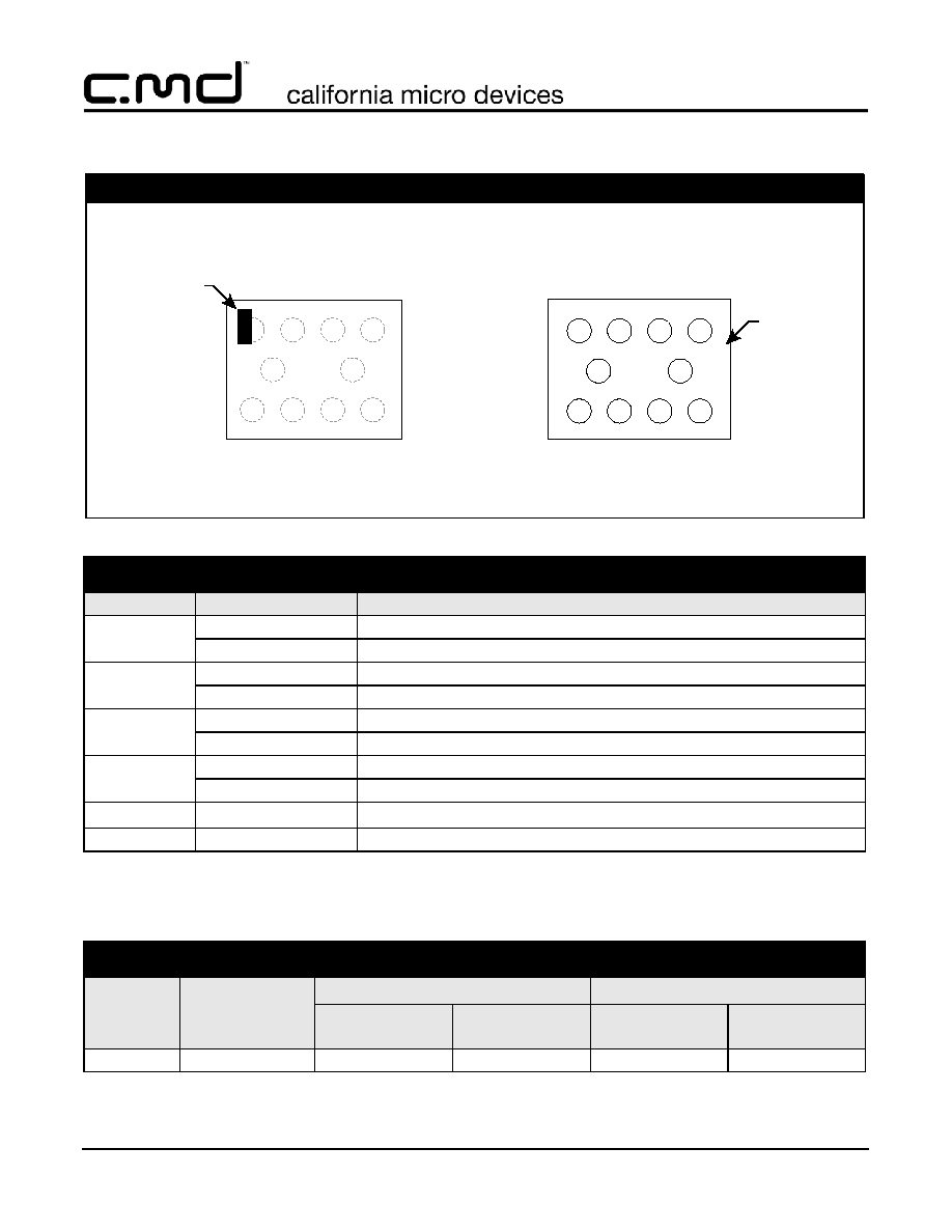
PIN DESCRIPTIONS
TYPE
PIN
DESCRIPTION
EMI
Filter
A1
EMI Filter with ESD Protection for RST Signal
C1
EMI Filter with ESD Protection for RST Signal
EMI
Filter
A2
EMI Filter with ESD Protection for CLK Signal
C2
EMI Filter with ESD Protection for CLK Signal
Device
Ground
B1
Device Ground
B2
Device Ground
EMI
Filter
A3
DAT EMI Filter with ESD Protection
C3
DAT EMI Filter with ESD Protection
ESD Channel
A4
ESD Proection Channel - V
CC
Supply
ESD Channel
C4
ESD Proection Channel
C3
C4
Orientation
Marking
C2
B1
B2
A2
A3
C1
A1
A4
A1
AG
3
1
4
2
C
B
A
Orientation
Marking
(see note 2)
PACKAGE / PINOUT DIAGRAMS
Notes:
TOP VIEW
CSPEMI400
CSP Package
BOTTOM VIEW
(Bumps Down View)
(Bumps Up View)
1) These drawings are not to scale.
2)
Lead-free devices are specified by using a "
+
" character for the top side orientation mark.
PART NUMBERING INFORMATION
Bumps
Package
Standard Finish
Lead-free Finish
2
Ordering Part
Number
1
Part Marking
Ordering Part
Number
1
Part Marking
10
CSP
CSPEMI400
AG
CSPEMI400G
AG
© 2005 California Micro Devices Corp. All rights reserved.
09/28/05
490 N. McCarthy Blvd., Milpitas, CA 95035-5112
Tel: 408.263.3214
Fax: 408.263.7846
www.cmd.com
3
CSPEMI400
Specifications
Note 1: T
A
=25
°
C unless otherwise specified.
Note 2: ESD applied to input and output pins with respect to GND, one at a time.
Note 3: Clamping voltage is measured at the opposite side of the EMI filter to the ESD pin. For example, if ESD is applied to Pin A1,
then clamping voltage is measured at Pin C1.
Note 4: Unused pins are left open
Note 5: The parameters are guaranteed by design.
ABSOLUTE MAXIMUM RATINGS
PARAMETER
RATING
UNITS
Storage Temperature Range
-65 to +150
°C
DC Power per Resistor
100
mW
DC Package Power Rating
300
mW
STANDARD OPERATING CONDITIONS
PARAMETER
RATING
UNITS
Operating Temperature Range
-40 to +85
°C
ELECTRICAL OPERATING CHARACTERISTICS
1
SYMBOL
PARAMETER
CONDITIONS
MIN
TYP
MAX
UNITS
R
1
Resistance of R
1
80
100
120
R
2
Resistance of R
2
38
47
56
C
Capacitance
V
IN
= 2.5VDC, 1MHz,
30mV ac
16
20
24
pF
V
STANDOFF
Stand-off Voltage
I = 10
A
6.0
V
I
LEAK
Diode Leakage Current
V
BIAS
= 3.3V
300
nA
V
SIG
Signal Voltage
Positive Clamp
Negative Clamp
I
LOAD
= 10mA
I
LOAD
= -10mA
5.6
-1.5
6.8
-0.8
9.0
-0.4
V
V
V
ESD
In-system ESD Withstand Voltage
a) Human Body Model, MIL-STD-883,
Method 3015
b) Contact Discharge per IEC
61000-4-2
Notes 2,4 and 5
±25
±10
kV
kV
V
CL
Clamping Voltage during ESD Discharge
MIL-STD-883 (Method 3015), 8kV
Positive Transients
Negative Transients
Notes 2,3,4 and 5
+12
-7
V
V
f
C1
Cut-off frequency
Z
SOURCE
= 50
, Z
LOAD
= 50
R = 100
, C = 20pF
77
MHz
f
C2
Cut-off frequency
Z
SOURCE
= 50
, Z
LOAD
= 50
R = 47
, C = 20pF
85
MHz
© 2005 California Micro Devices Corp. All rights reserved.
4
490 N. McCarthy Blvd., Milpitas, CA 95035-5112
Tel: 408.263.3214
Fax: 408.263.7846
www.cmd.com
09/28/05
CSPEMI400
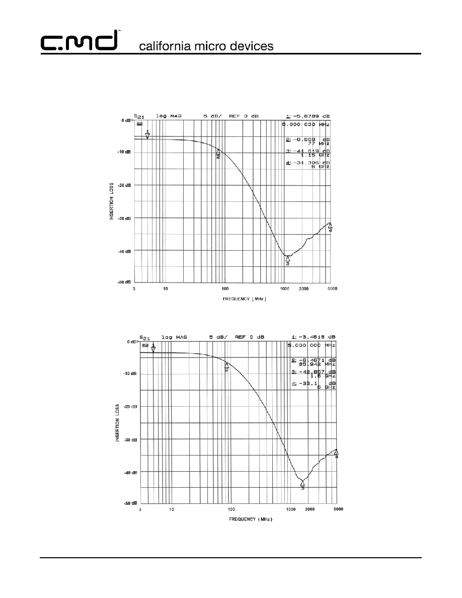
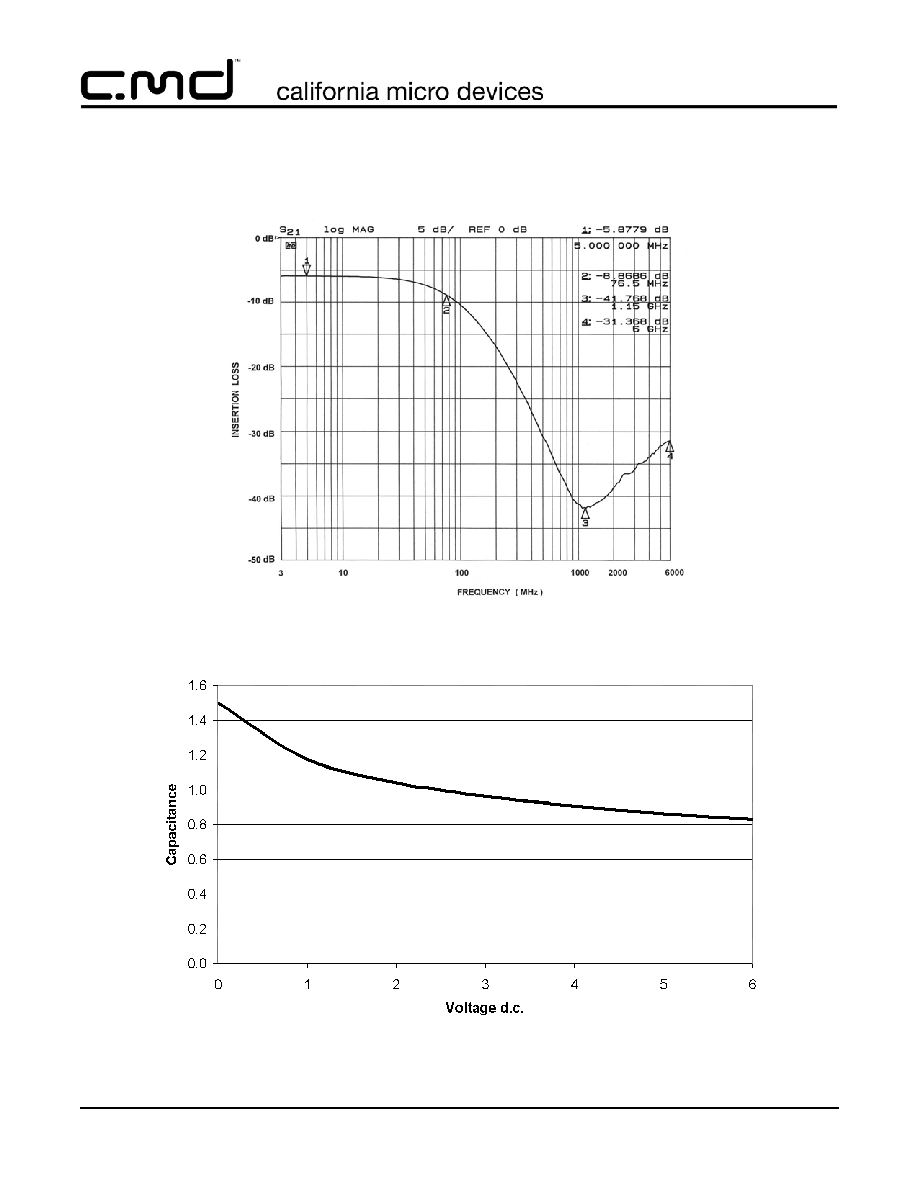
Performance Information
Typical Filter Performance (nominal conditions unless specified otherwise, 50 Ohm Environment)
Figure 1. A1-C1 EMI Filter Performance
Figure 2. A2-C2 EMI Filter Performance
© 2005 California Micro Devices Corp. All rights reserved.
09/28/05
490 N. McCarthy Blvd., Milpitas, CA 95035-5112
Tel: 408.263.3214
Fax: 408.263.7846
www.cmd.com
5
CSPEMI400
Performance Information (cont'd)
Typical Filter Performance (nominal conditions unless specified otherwise, 50 Ohm Environment)
Figure 3. A3-C3 EMI Filter Performance
Figure 4. Typical Diode Capacitance vs. Input Voltage (normalized to 2.5VDC)
Document Outline