 | ÐлекÑÑоннÑй компоненÑ: CSPESD301 | СкаÑаÑÑ:  PDF PDF  ZIP ZIP |
Äîêóìåíòàöèÿ è îïèñàíèÿ www.docs.chipfind.ru
© 2003 California Micro Devices Corp. All rights reserved.
12/10/03
430 N. McCarthy Blvd., Milpitas, CA 95035-5112
L Tel: 408.263.3214
L Fax: 408.263.7846 L www.calmicro.com
1
CSPESD301/302/303
1,2 and 3-Channel ESD Arrays in CSP
Features
·
1, 2 or 3 channels of ESD protection
·
±15kV ESD protection (IEC 61000-4-2, contact
discharge)
·
±30kV ESD protection (HBM)
·
Supports both AC and DC signal applications
·
Low leakage current (<100nA)
·
Chip Scale Package features extremely low lead
inductance for optimum ESD and filter perfor-
mance
·
4 bump, 1.06 x 0.93mm footprint Chip Scale Pack-
age (CSP)
·
Lead-free version available
Applications
·
I/O port protection
·
EMI filtering for data ports
·
Cellphones, notebook computers, PDAs
·
Wireless Handsets
·
MP3 Players
·
Digital Still Cameras
·
Handheld PCs
Product Description
The CSPESD301/302/303 is a family of 1, 2, and 3-
channel ESD protection arrays, which integrate two,
three and four identical avalanche-style diodes. It is
intended that one of these diodes is connected to GND
and the other diodes provide ESD protection for up to 3
lines depending upon the configuration utilized. The
back-to-back diode connections provide ESD protec-
tion for nodes that have AC signals up to 5.9V peak.
These devices provide a very high level of protection
for sensitive electronic components that may be sub-
jected to electrostatic discharge (ESD). The diodes
are designed and characterized to safely dissipate
ESD strikes of ±15kV, well beyond the maximum
requirements of the IEC 61000-4-2 international stan-
dard. Using the MIL-STD-883 (Method 3015) specifica-
tion for Human Body Model (HBM) ESD, these devices
protection against contact discharges at greater than
±30kV. The diodes also provide some EMI filtering,
when used in combination with a PCB trace or series
resistor.
These devices are particularly well suited for portable
electronics (e.g. cellular telephones, PDAs, notebook
computers) because of their small package format and
easy-to-use pin assignments.
The CSPESD301/2/3 is available in a space-saving,
low-profile, chip-scale package with optional lead-free
finishing.
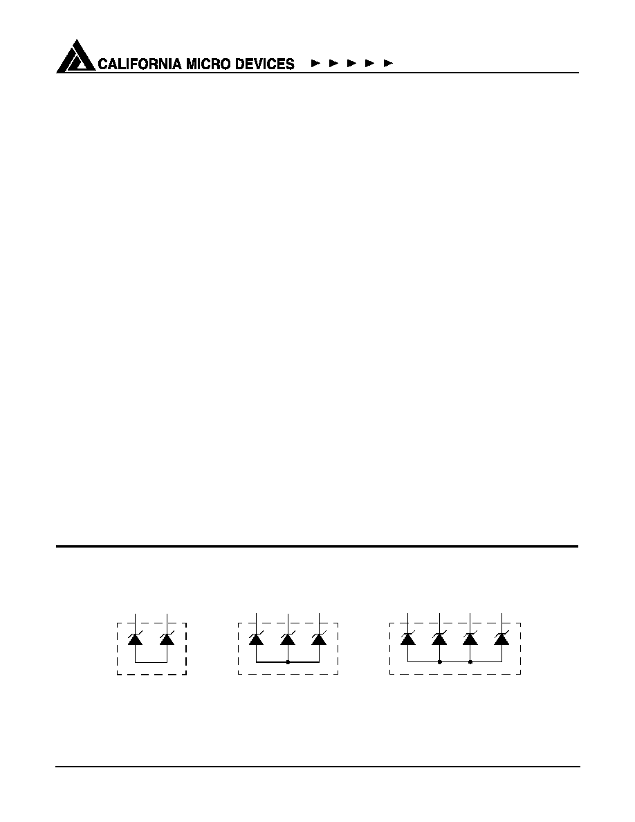
Electrical Schematics
B1
A2
B2
B1
A2
B2
B1
A2
A1
CSPESD301
CSPESD302
CSPESD303
© 2003 California Micro Devices Corp. All rights reserved.
2
430 N. McCarthy Blvd., Milpitas, CA 95035-5112
L Tel: 408.263.3214
L Fax: 408.263.7846 L www.calmicro.com
12/10/03
CSPESD301/302/303
Ordering Information
Note 1: Parts are shipped in Tape & Reel form unless otherwise specified.
Note 2: Lead-free devices are specified by using a "
+
" character for the top side orientation mark.
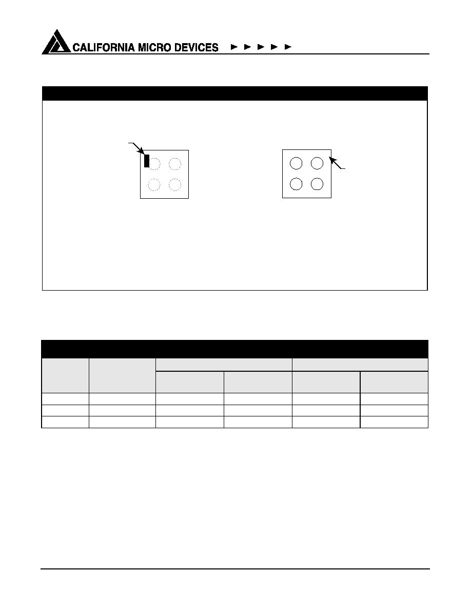
B2
B1
A1
A2
Orientation
Marking
A1
2
1
B
A
n*
Orientation
Marking
(see note 2)
PACKAGE / PINOUT DIAGRAMS
Notes:
CSPESD301/302/303
TOP VIEW
BOTTOM VIEW
(Bumps Down View)
(Bumps Up View)
* See ordering information for
appropriate part marking.
1) These drawings are not to scale.
2) Lead-free devices are specified by using a "+" character for the top side orientation mark.
4-Bump CSP Package
3) All 4 bumps are always present. Unused bumps are electrically unconnected.
PART NUMBERING INFORMATION
Bumps
Package
Standard Finish
Lead-free Finish
2
Ordering Part
Number
1
Part Marking
Ordering Part
Number
1
Part Marking
4
CSP
CSPESD301
F
CSPESD301G
F
4
CSP
CSPESD302
G
CSPESD302G
G
4
CSP
CSPESD303
H
CSPESD303G
H
© 2003 California Micro Devices Corp. All rights reserved.
12/10/03
430 N. McCarthy Blvd., Milpitas, CA 95035-5112
L Tel: 408.263.3214
L Fax: 408.263.7846
L www.calmicro.com
3
CSPESD301/302/303
Specifications
Note 1: T
A
=25
°
C unless otherwise specified.
Note 2: ESD applied to input and output pins with respect to
another diode, one at a time.
Note 3: Unused pins are left open.
Note 4: These parameters are guaranteed by design and char-
acterization.
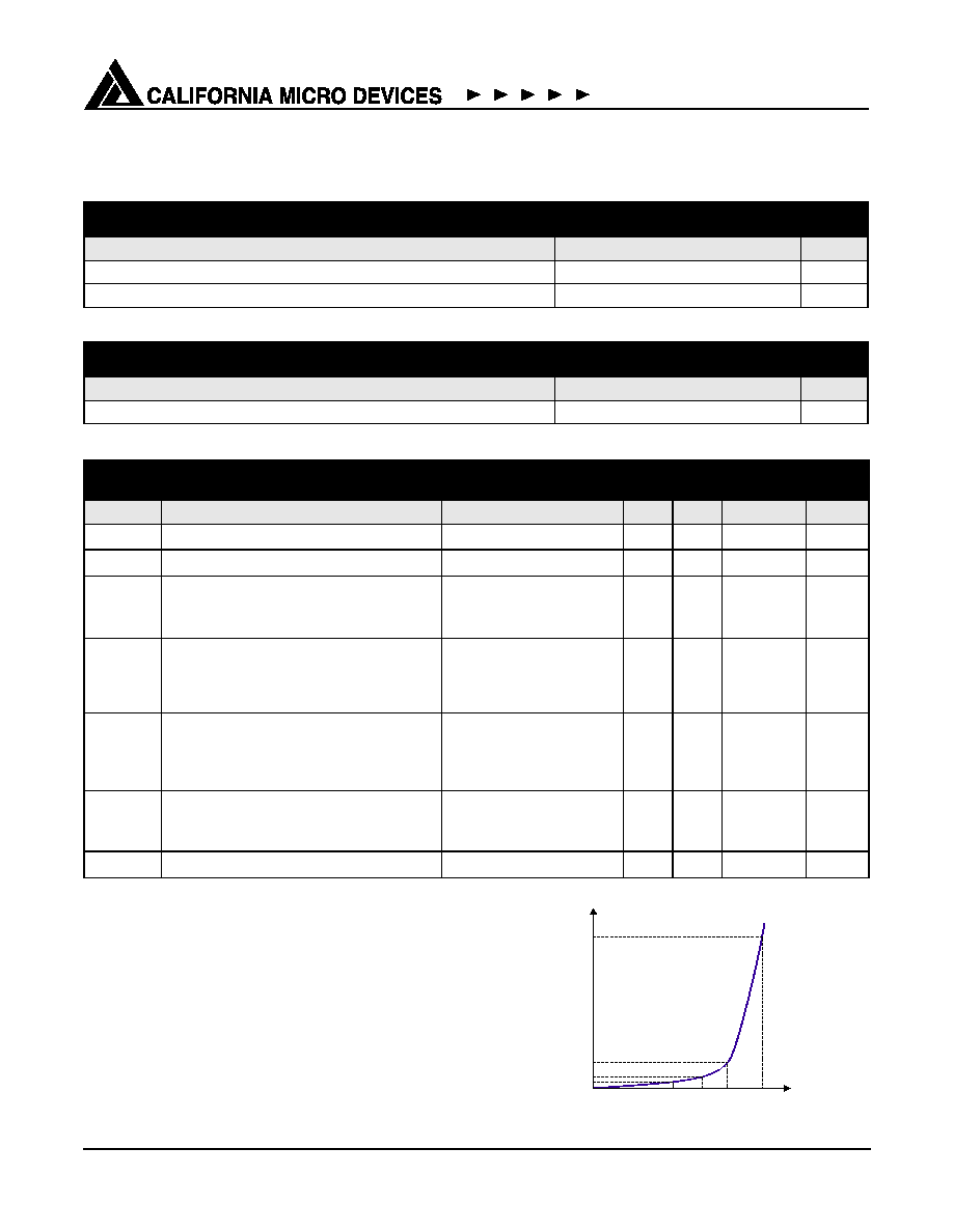
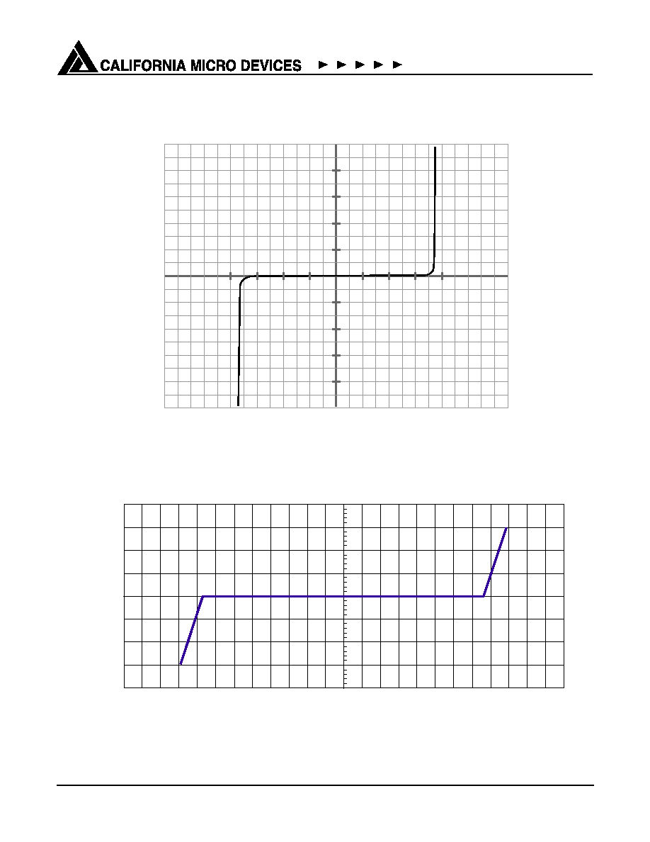
Figure 1. Parameter Legend
ABSOLUTE MAXIMUM RATINGS
PARAMETER
RATING
UNITS
Storage Temperature Range
-65 to +150
°C
DC Package Power Rating
200
mW
STANDARD OPERATING CONDITIONS
PARAMETER
RATING
UNITS
Operating Temperature Range
-40 to +85
°C
ELECTRICAL OPERATING CHARACTERISTICS
1
SYMBOL
PARAMETER
CONDITIONS
MIN
TYP
MAX
UNITS
V
SO
Diode Stand-off Voltage
I
DIODE
=
±10µA
±5.9
V
I
LEAK
Diode Leakage Current
V
IN
=3.3V
100
nA
V
SIG
Small Signal Clamp Voltage
Positive Clamp
Negative Clamp
I
DIODE
= 10mA
I
DIODE
= -10mA
6.0
-9.2
7.6
-7.6
9.2
-6.0
V
V
V
ESD
In-system ESD Withstand Voltage
a) Human Body Model, MIL-STD-883,
Method 3015
b) Contact Discharge per IEC 61000-4-2
Notes 2, 3 and 4
±30
±15
kV
kV
V
CL
Clamping Voltage during ESD Discharge
MIL-STD-883 (Method 3015), 8kV
Between adjacent bumps
Between diagonal bumps
Notes 2, 3 and 4
19.5
19.9
V
V
R
D
Dynamic Resistance
Between adjacent bumps
Between diagonal bumps
Notes 2, 3 and 4
0.85
1.10
C
Capacitance
At 0VDC, 1MHz, 30mVAC
27
pF
3.3V
10mA
10µA
V
SIG
V
CL
V
I
ESD
I
LEAK
slope = 1
/
R
D
V
SO
I
© 2003 California Micro Devices Corp. All rights reserved.
4
430 N. McCarthy Blvd., Milpitas, CA 95035-5112
L Tel: 408.263.3214
L Fax: 408.263.7846 L www.calmicro.com
12/10/03
CSPESD301/302/303
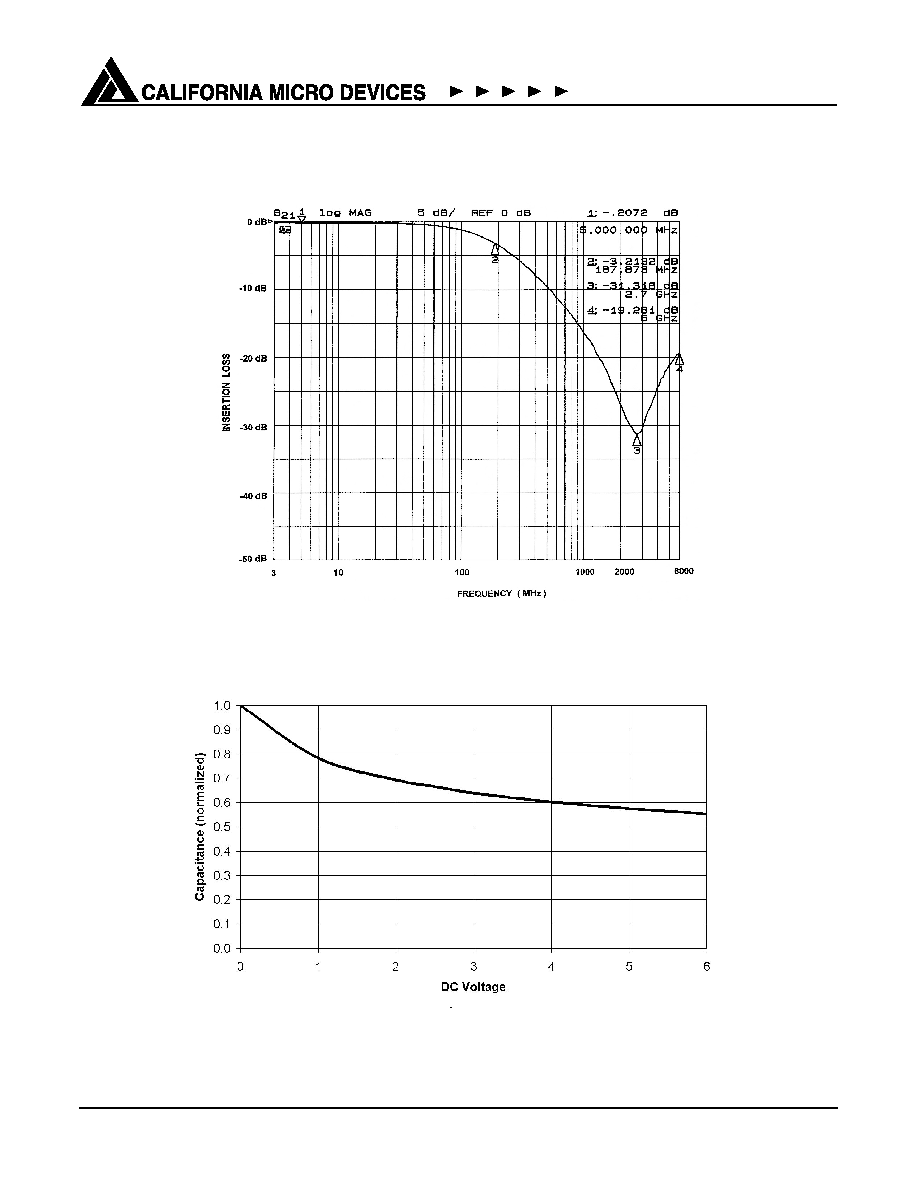
Performance Information
Figure 2. Typical EMI Filter Performance (0VDC, 50 Ohm Environment)
Figure 3. Typical Capacitance VS. Input Voltage (normalized to 0Vdc)
© 2003 California Micro Devices Corp. All rights reserved.
12/10/03
430 N. McCarthy Blvd., Milpitas, CA 95035-5112
L Tel: 408.263.3214
L Fax: 408.263.7846
L www.calmicro.com
5
CSPESD301/302/303
Performance Information (cont'd)
Figure 4. Low Current I-V Curve
Figure 5. High Current I-V Curve
2
2
4
6
8
-6
-4
-2
4
6
8
-8
-6
-4 -2
I (µA)
V (V)
-8
-2.0
-1.5
-1.0
-0.5
0.0
0.5
1.0
1.5
2.0
-12 -11 -10 -9
-8
-7
-6
-5
-4
-3
-2
-1
0
1
2
3
4
5
6
7
8
9
10 11 12
High Current I-V Characteristic - Pads A1 to A2
Current [A]
Voltage [V]
Document Outline